- Here are schematic diagrams of different Commodore devices.
You may also want to visit http://www.agtannenbaum.com/ (USA) or
http://www.schaltungsdienst.com/ (Germany) who sell service manuals
and schematic diagrams for various devices.
- ALLFILES
- Index of all files under the /pub/cbm/schematics tree, text version.
- ALLFILES.html
- CBM_part_numbers_19870601.PDF
- CBM Parts list for June, 1987
- Commodore_Parts_Cross_Reference_Manual.pdf
- Parts/ic cross reference 1985 PN-314000-01
Index of all files under the /pub/cbm/schematics tree, HTML version.
- cartridges/
- Cartridges for various computers
- c128/
- diag@ (link)
- c64/
- External cartridges for the Commodore 64
- cie.gif
- Reverse engineered schematic diagram of an IEEE-488 cartridge, drawn
by William Levak. See also ../vic20/ieee-488/vie.gif.
- cpm/
- The Commodore 64 CP/M cartridge has a Z80 processor running at 1 MHz.
The schematic diagram of the cartridge was reverse-engineered by
Ruud Baltissen. There is also some documentation on this cartridge in
early prints of the Commodore 64 Programmer's Reference Guide. In later
prints, the pages that originally described the CP/M cartridge were
left blank.
- README
- Ruud Baltissen's technical overview of the CP/M cartridge and some comments.
- c64_cpm_cartridge.zip
- Timing and power information about the CP/M cartridge
- schematics.gif
- Schematic Diagram, drawn by Ruud Baltissen
- schematics.hdf
- schematics.sch
- UltiCap files of the cartridge, drawn by Ruud Baltissen. These *might* have an
error in them around U2B and U2F. Please confirm them with schematics.gif before
using.
- z80.gif
- Another reverse engineered schematic diagram of the Z80 cartridge.
Drawn by Jerzy Sobola, January 26, 1999.
Downloaded from http://www.republika.pl/jsobola/schematy.htm.
- demodisks@ (link)
- demodisks@ (link)
- diag/
- C64DiagHarnass.pdf
- Peter Schepers drawing of diag harnass schematics
- blackbox.bin
- Firmware for the Blackbox cartridge.
- blackbox.gif
- Reverse engineered schematic diagram of Blackbox, a Polish
cartridge that seems to contain some hardware diagnostics.
Drawn by Jerzy Sobola, July 2, 1999. Downloaded from
http://www.republika.pl/jsobola/schematy.htm.
- diag-c64-4k.bin
- Firmware for a 4-kilobyte diagnostic cartridge.
Downloaded from http://www.republika.pl/jsobola/schematy.htm.
- diag-c64-4k.gif
- Reverse engineered schematic diagram of a 4-kilobyte diagnostic cartridge
and its test harnesses. Drawn by Jerzy Sobola, July 23, 1999.
Downloaded from http://www.republika.pl/jsobola/schematy.htm.
- diag-c64-8k.bin
- Firmware for a 8-kilobyte diagnostic cartridge.
Downloaded from http://www.republika.pl/jsobola/schematy.htm.
Independently provided by Raymond Carlsen.
- diag-c64-8k.gif
- Reverse engineered schematic diagram of a 8-kilobyte diagnostic cartridge
and its test harnesses. Drawn by Jerzy Sobola, March 12, 1999.
Downloaded from http://www.republika.pl/jsobola/schematy.htm.
- diag-c64-8k.txt
- Raymond Carlsen's notes on the 8-kilobyte diagnostic cartridge.
- diag2@ (link)
- freezer/
- Freezer cartridges allow the running program to be stopped, so that
memory images can be backed up, modified or restored.
- KCSPowerCartridgeSchematic.pdf
- KCS Freezer Cart schematic. See http://commodore.edkhome.nl/hwproj/kcspower/
- MK.gif
- MK7PLA.txt
- Schematic diagram of an Action Replay freezer cartridge clone, and the
contents of the PLA chip required for the cartridge.
- action73.bin
- Firmware for "Action Plus v. 7.3". The texts are in German.
- action73.gif
- Reverse engineered schematic diagram of "Action Plus v. 7.3". This
looks like an Action Replay freezer cartridge by Datel.
Drawn by Jerzy Sobola, July 2, 1999. Downloaded from
http://www.republika.pl/jsobola/schematy.htm.
- fc1.gif
- Schematic diagram of the Final Cartridge I.
- fc3.gif
- Schematic diagram of the Final Cartridge III.
- ieee-488/
- Commodore's IEEE-488 cartridge for the Commodore 64. Reverse-engineered
by Wolfgang Günther <woll@wolltronic.de>.
- README
- Description of the interface, including hints to design errors of the
original interface
- eprom.bin
- The firmware (4 kB, raw binary)
- schematics.ps
- Schematic diagram of the interface in PostScript format
- schematics.tif
- Schematic diagram of the interface in TIFF format
- magic-voice/
- The Commodore Magic Voice cartridge is a speech synthesizer with a very
limited vocabulary of English. For more information about the cartridge,
see http://calvin.ptloma.edu/%7Espectre/ckb/secret/operiph.html.
- 251476.bin
- Firmware of the Commodore Magic Voice cartridge, read from an EPROM.
The high part of the ROM is mapped into $E000-$FFFF, the low part into
$A000-$BFFF.
- schematic.pdf
- Schematic diagram of the Commodore Magic Voice cartridge. Drawn by
Joachim Nemetz http://nemetzpower.de/.
- sfx/
- The Commodore SFX Sound Expander was designed by Richard Watts of
Music Sales Ltd and sold by Commodore as part of the 'Commodore SFX'
product line. The cartridge uses an FM synthesis chip, the YM3256 OPL,
which is similar to the YM3812 OPL2 chip used in the AdLib and
SoundBlaster cards for IBM PC compatibles.
- analogue.jpg
- Analogue part of the Sound Expander, reverse-engineered and
hand-drawn by Richard Atkinson.
- digital.jpg
- Digital interface of the Sound Expander, reverse-engineered and
hand-drawn by Richard Atkinson.
- sfx-sch.gif
- Schematic for the Commodore C64/C128 Sounder Expander cartridge.
Both analogue and digital parts; reverse-engineered.
- demodisks@ (link)
- userport@ (link)
- pet/
- Commodore PET add-ons
- ada1800.gif
- Reverse engineered schematic diagram of the ADA 1800 PET printer interface.
The interface is connected to the IEEE-488 port, and some discrete logic
converts the signals to Centronics.
Drawn by Jerzy Sobola, July 22, 1999. Downloaded from
http://www.republika.pl/jsobola/schematy.htm.
- modempet.gif
- Reverse engineered schematic diagram of a 300 baud modem for the PET
user port, Mark VII Auto 232. Drawn by Jerzy Sobola, February 11, 1999.
Downloaded from http://www.republika.pl/jsobola/schematy.htm.
- petDiagHardwareClip.zip
- Schematics of diagnostic clip for PET computers by Ken McIlveen
- petsound.gif
- Reverse engineered schematic diagram of a PET sound interface KL-4M
that connects to the user port and to the cassette port. It seems to
have a 8-bit D/A converter and a speaker. Drawn by Jerzy Sobola,
January 1, 1999. Downloaded from
http://www.republika.pl/jsobola/schematy.htm.
- plus4/
- Cartridges for the Commodore 264 series (C16, C116 and plus/4)
- speedy.bin
- Firmware for the Speedy freezer cartridge.
- speedy.gif
- Reverse engineered schematic diagram of a Speedy freezer cartridge.
Drawn by Jerzy Sobola, January 23, 1999. Downloaded from
http://www.republika.pl/jsobola/schematy.htm.
- userport/
- Cartridges for the user port (Commodore 64 and VIC-20)
- 1011005.gif
- VIC-1011 RS-232C adapter rev.A, assy number 1011005.
- eprburn.gif
- Reverse engineered schematic diagram of an EPROM burner for the C64/C128.
Drawn by Jerzy Sobola, January 23, 1999. Downloaded from
http://www.republika.pl/jsobola/schematy.htm.
- modem/
- Commodore telephone modems (VICMODEM, 1650, 1660, 1670 et al) are
plugged into the user port.
- chips.txt
- List of integrated circuits in the Commodore modems. Composed by
William Levak.
- switches.txt
- DIP switch settings in various Commdore modem models. Composed by
William Levak.
- vic20/
- Cartridges for the VIC-20
- vic20cvc.bin
- Firmware of the Color Video Controller cartridge.
Downloaded from http://www.republika.pl/jsobola/schematy.htm.
- vic20cvc.gif
- Reverse engineered schematic diagram of a Color Video Controller device
(scrolling text interface) that plugs to the cartridge port and to the
user port. Drawn by Jerzy Sobola, January 26, 2001.
Downloaded from http://www.republika.pl/jsobola/schematy.htm.
- ieee-488/
- CBM IEEE-488 cartridges
VIC-1112 reverse-engineered by Wolfgang Günther <woll@wolltronic.de>
- 1110010.png
- Schematic diagram, IEEE-488 interface board, K. Takagi, 2/5/81,
CBM Osaka, Japan, 1110010 rev. A, used on VC-1112.
- 325329-04.bin
- Firmware for the VIC-1112 (325329-03 has the same contents)
- README
- Description of the VIC-1112 interface and of the schematic diagrams
- schematics.ps
- VIC-1112 Schematic diagram of the interface in PostScript format.
Reverse engineered by Wolfgang Günther.
- schematics.tif
- Conversion of the VIC-1112 file schematics.ps in TIFF format.
- vie-rom-9c00.prg
- Firmware for VIE IEEE-488 cartridge, @$9c00, started with sys 40000
- vie.gif
- Reverse engineered schematic diagram of an IEEE-488 cartridge, drawn by
William Levak. See also ../../c64/cie.gif.
- userport@ (link)
- computers/
- Here are schematic diagrams of different Commodore computers.
Many of these directories also contain service and Tech manuals
- Z8000_Schematics.pdf
- Schematics of the Commodore 900 (Z8000) computer.
- clcd.pdf
- Schematics to C= LCD 8-bit laptop, from Bil Herd with thanks to Steve Gray and
Mike Naberezny
- b/
- The Commodore Model B service manual and schematic diagrams
- 314010-06-i.gif
- Service manual, B model computer: (Jan. 1985, PN-314010-06), title page
- 314010-06-ii.gif
- Service manual, B model computer: table of contents
- 314010-06-p1.gif
- Service manual, B model computer: Page 1: block diagram
- 314010-06-p2.gif
- Service manual, B model computer: Page 2: B model parts list
- 314010-06-p3-left.gif
- Service manual, B model computer: Page3: 8256048 board left side
- 314010-06-p3-right.gif
- Service manual, B model computer: Page 3: 8256048 board right side
- 314010-06-p4.gif
- Service manual, B model computer: Page 4: 8256048 PCB parts
- 314010-06-p5.gif
- Service manual, B model computer: Page 5: 8256048 PCB parts, continued
- 314010-06-p6-left.gif
- Service manual, B model computer: Page 6: keyboard matrix left side
- 314010-06-p6-right.gif
- Service manual, B model computer: Page 6: keyboard matrix right side
- 4256004-01-left.gif
- Commodore CBM-II B model Switching power supply, left side
- 4256004-01-parts.gif
- Commodore CBM-II B model Switching power supply, Parts list
- 4256004-01-right.gif
- Commodore CBM-II B model Switching power supply, right side
- 4256041-01of15.gif
- Commodore P500 Color Computer: address & data buffers, arbitration logic
- 4256041-02of15.gif
- Commodore P500 Color Computer: system decode & buffer control
- 4256041-03of15.gif
- Commodore P500 Color Computer: VIC; video memory; video bus buffers
- 4256041-04of15.gif
- Commodore P500 Color Computer: SID; 192k DRAM array refresh logic
- 4256041-05of15.gif
- Commodore P500 Color Computer: 192k DRAM address mux & control
- 4256041-06of15.gif
- Commodore P500 Color Computer: 192k*8 DRAM array [64k standard, 128k optional]
- 4256041-07of15.gif
- Commodore P500 Color Computer: 64k DRAM array and address mux
- 4256041-08of15.gif
- Commodore P500 Color Computer: system ROM/RAM array
- 4256041-09of15.gif
- Commodore P500 Color Computer: gameport interface; keyboard interface; RS232C interface
- 4256041-10of15.gif
- Commodore P500 Color Computer: interrupt prioritization; IEEE488 interface; user/game port interface
- 4256041-11of15.gif
- Commodore P500 Color Computer: cassette i/f port
- 4256041-12of15.gif
- Commodore P500 Color Computer: main oscillators & PLL
- 4256041-13of15.gif
- Commodore P500 Color Computer: video output circuit
- 4256041-14of15.gif
- Commodore P500 Color Computer: [List of power filter capacitors for each IC]
- 4256041-15of15.gif
- Commodore P500 Color Computer: [FPLA logic equations]
- 4256047-01.jpg
- 4256047-02.jpg
- 4256047-03.jpg
- CBM-II z80 board schematic.
- 8088.gif
- 8088.txt
- The 8088 co-processor board for B-series machines. Reverse engineered
by Ruud Baltissen http://ruud.c64.org.
- 8256043-01of14-left.gif
- CBM-II LP: schematic P1, left side: address & data buffers, bus arbitration
- 8256043-01of14-right.gif
- CBM-II LP: schematic P1, right side: address & data buffers, bus arbitration
- 8256043-02of14-left.gif
- CBM-II LP: schematic P2, left side: master timing
- 8256043-02of14-right.gif
- CBM-II LP: schematic P2, right side: master timing
- 8256043-03of14-left.gif
- CBM-II LP: schematic P3, left side: DRAM address & refresh
- 8256043-03of14-right.gif
- CBM-II LP: schematic P3, right side: DRAM address & refresh
- 8256043-04of14-left.gif
- CBM-II LP: schematic P4, left side: DRAMs, segments 1-2
- 8256043-04of14-right.gif
- CBM-II LP: schematic P4, right side: DRAMs, segments 1-2
- 8256043-05of14-left.gif
- CBM-II LP: schematic P5, left side: DRAMs, segments 3-4
- 8256043-05of14-right.gif
- CBM-II LP: schematic P5, right side: DRAMs, segments 3-4
- 8256043-06of14-left.gif
- CBM-II LP: schematic P6, left side: ROM array, 1k×8 static RAM
- 8256043-06of14-right.gif
- CBM-II LP: schematic P6, right side: ROM array, 1k×8 static RAM
- 8256043-07of14-left.gif
- CBM-II LP: schematic P7, left side: system decode
- 8256043-07of14-right.gif
- CBM-II LP: schematic P7, right side: system decode
- 8256043-08of14-left.gif
- CBM-II LP: schematic P8, left side: CRTC, video shift register
- 8256043-08of14-right.gif
- CBM-II LP: schematic P8, right side: CRTC, video shift register
- 8256043-09of14-left.gif
- CBM-II LP: schematic P9, left side: video RAM, address mux, latch
- 8256043-09of14-right.gif
- CBM-II LP: schematic P9, right side: video RAM, address mux, latch
- 8256043-10of14-left.gif
- CBM-II LP: schematic P10, left side: keyboard port, RS232C
- 8256043-10of14-right.gif
- CBM-II LP: schematic P10, right side: keyboard port, RS232C
- 8256043-11of14-left.gif
- CBM-II LP: schematic P11, left side: user I/O ports, IEEE
- 8256043-11of14-right.gif
- CBM-II LP: schematic P11, right side: user I/O ports, IEEE
- 8256043-12of14-left.gif
- CBM-II LP: schematic P12, left side: SID, dot clock oscillator, expansion connector
- 8256043-12of14-right.gif
- CBM-II LP: schematic P12, right side: SID, dot clock oscillator, expansion connector
- 8256043-13of14.gif
- CBM-II LP: schematic P13: video output, power indicator
- 8256043-14of14.gif
- CBM-II LP: schematic P14: I.C. count, power consumption
- 8256059-01.gif
- CBM-II HP: schematic P1: address and data bus arbitration
- 8256059-02.gif
- CBM-II HP: schematic P2: master timing
- 8256059-03.gif
- CBM-II HP: schematic P3: dram address and refresh
- 8256059-04.gif
- CBM-II HP: schematic P4: dram segment 1 and 2
- 8256059-05.gif
- CBM-II HP: schematic P5: dram segment 3 and 4
- 8256059-06.gif
- CBM-II HP: schematic P6: rom array, 1kx8 static rom
- 8256059-07.gif
- CBM-II HP: schematic P7: system decode
- 8256059-08.gif
- CBM-II HP: schematic P8: crtc, video shift reg outputs
- 8256059-09.gif
- CBM-II HP: schematic P9: video ram, address mux, latch
- 8256059-10.gif
- CBM-II HP: schematic P10: keyport port1 rs232c
- 8256059-11.gif
- CBM-II HP: schematic P11: user i/o ports, ieee-488
- 8256059-12.gif
- CBM-II HP: schematic P12: sid, casette, dotclk osc, expanse
- CBM-II-partial700Schematic.zip
- Contains partial schematic of CBM 7xx series, drawn by Ruud Baltissen
- CBM700_CRT_Schematics.pdf
- Schematics for CRT board used in CBM 700 series, as well as the CBM 128-80 and
256-80
- CBM_8088_CPU_co-processor_schematic.pdf
- Schematic to 8088 option card for CBM-II machines.
- README
- General information about the Commodore Model II computers.
- README500
- Information about the Commodore 500 a.k.a. PET II.
- cbm-610-psu-german.jpg
- CBM 610 Power Supply schematic, uploaded by Christian Forstreuter
- cbm2-schematics-4256004-01-lp-ps.pdf
- Commodore CBM-II B model Switching power supply, full schematic
- cbm2-schematics-8256043-bl.pdf
- CBM-II LP Full Schematic doc
- cbm2_hires_color_graphic_1_of_4.png
- cbm2_hires_color_graphic_2_of_4.png
- cbm2_hires_color_graphic_3_of_4.png
- cbm2_hires_color_graphic_4_of_4.png
- Schematic of unknown CBM-II Hi-Res Graphic something
- cbm500-700keyboardAdapter.jpg
- Pinout useful to adapting a B500 keyboard for the B700 series. From Alessandro
Liberalto
- cbm700_CEAG_Supply_C.pdf
- cbm700_CEAG_Supply_D-F.pdf
- cbm700_CEAG_Supply_US-B.pdf
- Schematic of B7x0 power supplies, drawn by Christian Forstreuter
** Note: The TDA 1060 pin 13 (over-voltage prot input) is
floating on many of these supplies, which can lead to failure. The
recommendation is to ground it to pin 12 if that is the case.
- cbm700keyboardPinout.gif
- cbm 700 (HP) keyboard pinout (by Liberalato Alessandro)
- p500-keyboard.txt
- Commodore P500 Keyboard Schematic. Composed by Tony Duell
<ard@p850ug1.demon.co.uk>.
- parts.txt
- Parts list for CBM-II series computers, from William Levak
- drives@ (link)
- firmware@ (link)
- c128/
- The Commodore 128 existed in three different major board versions:
The first board was used in the flat 128 and in the plastic-cased 128D.
Then came the 128DCR board, with the floppy controller integrated on the
motherboard. There was also a 128CR (cost-reduced flat 128).
- 310378-1-left-and-right.gif
- 310378-2-left-and-right-7a.gif
- 310378-2-left-and-right.gif
- 310378-3-left-and-right-7a.gif
- 310378-3-left-and-right.gif
- 310378-4-left-and-right.gif
- These are the schematic diagrams of the Commodore 128 main board
("flat C128" and C128D in plastic case). They were on eight pages
in the Commodore 128 Programmer's Reference Guide, two pages
containing one engineering sheet.
- 310378-update.zip
- Update to the Commodore 128 Service Manual, containing the two revised
pages in the 310378 schematic revision 7A.
- 8721-pla.v
- 8721 PLA in Verilog by Johan Grip
- c128cr.jpg
- A black&white picture of a cost-reduced flat Commodore 128 circuit board.
This model never entered mass production; this is an engineering sample
possessed by Raymond Carlsen. The board says "PCB ASSY NO. 250783",
"C= commodore C128CR REV.3", "PCB NO. 252270", and "C128CR No.2
ENG. SAMPLE Jun/9/'86 KNT".
- c128dcr-1-left_and_right.gif
- c128dcr-2-left_and_right.gif
- c128dcr-3-left_and_right.gif
- c128dcr-4-left_and_right.gif
- c128dcr-5-left_and_right_corrected.gif
- These are the schematic diagrams of the Commodore 128DCR main board
(metal case C128D with built-in 1571CR floppy controller). The diagrams
were scanned from a 64'er Sonderheft, and they appear to be a copy of
schematic 252451.
According to Nicolas Welte, there is an error on the right half of page 5.
The 74LS14 hex Schmitt-trigger inverter U113, pin 13 is connected to WPRT*
(misprinted WTRT* on U105), which doesn't make any sense. Obviously it
should be connected to STP1 instead, which is three lines more to the right!
- c128schematic.gif
- C128 schematic, unknown rev, drawn by unknown author.
- mainboardC128_rev7.png
- Hi-res picture of 128 main board traces, without chips.
- parts.txt
- Parts list for Commodore 128, from William Levak
- drives@ (link)
- firmware@ (link)
- power/
- Power supplies of the Commodore 128 computers
Scanned by Martin Buchty, uploaded by Oliver Weissflach,
improved by William Levak
- ps-128.gif
- External switching power supply for the flat Commodore 128. This looks
like a hand-made copy of the Mitsumi power supply schematic, Commodore
part number 252449-01, page 78 of the service manual.
- ps-128d-german.gif
- Internal switching power supply for the 128D (plastic case), German version
(Schaffer BV 223-5-04008)
- ps-128d-japanese.gif
- Internal switching power supply for the 128D (plastic case), Japanese version
(Nagano Japan Radio Co. Ltd, 310639-03, NJD-1978)
- ps-128dcr-usa.gif
- Internal switching power supply for the 128DCR (metal case), USA version;
includes measurement points and expected waveforms
- ps-128dcr1.gif
- Internal switching power supply for the 128DCR (metal case), 1st version
(linearly regulated 12 volts DC output)
- ps-128dcr2.gif
- Internal switching power supply for the 128DCR (metal case), 2nd version
(Tohoku Metal Industries 1403Et, 5628-C001-00)
- servicemanuals/
- C128D-1571_Diagnostic_Manual_v1.2_1.3_314855-03_1988_Oct.pdf
- C128_Developers_Package_for_Commodore_6502_Development_(1987_Oct).pdf
- C128_Diagnostic_Instruction_and_Troubleshooting_Manual_(314060-01-02).pdf
- Commodore_128_128D_Service_Manual_1987_Nov.pdf
- Commodore_128_128D_Service_Manual_314001-08_(1987_Nov).pdf
- Commodore_128_128D_Service_Manual_314001-08_(1987_Nov)_Alt_Ver.pdf
- Commodore_128_Service_Manual_Preliminary_314001-07_(1985_Aug)_(missing_pages_26-45).pdf
- manual/
- Service Manual C-128/C128D Computer, November 1987, PN-314001-08
- 00-title.gif
- Title page
- 00.gif
- Table of contents
- 01.gif
- Specifications
- 02.gif
- Parts list
- 03.gif
- Block diagram (wide sheet)
- 04.gif
- Bus architecture
- 05.gif
- 06.gif
- 8502 microprocessor
- 07.gif
- 08.gif
- Z-80 microprocessor
- 09.gif
- 10.gif
- 11.gif
- Memory architecture
- 12.gif
- 13.gif
- 14.gif
- 15.gif
- Read Only Memory
- 16.gif
- 17.gif
- Random Access Memory
- 18.gif
- 19.gif
- 20.gif
- Memory Management Unit
- 21.gif
- 22.gif
- 23.gif
- 24.gif
- 25.gif
- 26.gif
- 27.gif
- 28.gif
- Programmed Logic Array
- 29.gif
- 30.gif
- 8701 clock generator
- 31.gif
- Video interface
- 32.gif
- 33.gif
- 8564 Video Interface Chip
- 34.gif
- 35.gif
- 36.gif
- 8563 Video Controller
- 37.gif
- 38.gif
- 39.gif
- 8568 CRT Controller
- 40.gif
- 41.gif
- 8580 Sound Interface Device
- 42.gif
- 43.gif
- 44.gif
- 45.gif
- 46.gif
- 47.gif
- Floppy disk drive read/write head amplifier
- 48l.gif
- 48r.gif
- 49.gif
- Input/Output circuits: Cassette interface
- 50.gif
- 51.gif
- Keyboard
- 52.gif
- Expansion bus
- 53.gif
- 54.gif
- Serial bus
- 55.gif
- 56.gif
- Troubleshooting: Common line definitions
- 57.gif
- Common ICs (pin assignments and logic)
- 58.gif
- 59.gif
- 60.gif
- 61.gif
- 62.gif
- 63.gif
- Board layout, PCB assy #310379 revision 6. Identifying factor:
On solder side of board at the expansion bus, CN1, the artwork
#310381 rev. 6 appears.
- 64.gif
- PCB assembly #310379 rev. 6
- 65.gif
- 66l.gif
- 66r.gif
- I/O - Control Ports, Keyboard, User Port, Serial Port, Cassette Port
Schematic 310378 rev. 6, sheet 1 of 4
- 67l.gif
- 67r.gif
- Microprocessors, MMU, SID, PLA, power supply
Schematic 310378 rev. 6, sheet 2 of 4
- 68l.gif
- 68r.gif
- Video, Clock, Reset
Schematic 310378 rev. 6, sheet 3 of 4
- 69l.gif
- 69r.gif
- RAM, ROM
Schematic 310378 rev. 6, sheet 4 of 4
- 70.gif
- Board layout, PCB ASSY #310379 revision 7. Identifying factor:
On solder side of board at the expansion bus, CN1, the artwork
#310381 rev. 7 appears.
- 71.gif
- PCB assembly #310379 rev. 7
- 72.gif
- 73l.gif
- Quick reference (table of topics and page numbers)
- 73r.gif
- I/O - control ports, keyboard, user port, serial port, cassette port
Schematic 310378 rev. 7, sheet 1 of 4
- 74l.gif
- Quick reference (table of topics and page numbers)
- 74r.gif
- Microprocessors, MMU, SID, PLA, power supply
Schematic 310378 rev. 7A, sheet 2 of 4
- 75l.gif
- Quick reference (table of topics and page numbers)
- 75r.gif
- Video, clock, reset
Schematic 310378 rev. 7A, sheet 3 of 4
- 76l.gif
- Quick reference (table of topics and page numbers)
- 76r.gif
- RAM, ROM
Schematic 310378 rev. 7, sheet 4 of 4
- 77.gif
- RF modulator
- 78.gif
- Power supply schematic - for reference only: Mitsumi - PN-252449-01
- 79.gif
- Power supply schematic - for reference only: Dee-Van - PN-252449-03
- 80l.gif
- C128D major parts
- 80r.gif
- Service parts reference diagram: "explosion diagram" of the C128DCR
- 81l.gif
- Componets (sic) parts list - PCB assembly 250477
- 81r.gif
- Board layout - PCB assembly 250477-01 (C128DCR)
- 82.gif
- Schematic 252451, sheet 1 of 5
- 83.gif
- Schematic 252451, sheet 2 of 5
- 84.gif
- Schematic 252451, sheet 3 of 5
- 85.gif
- Schematic 252451, sheet 4 of 5
- 86.gif
- index.html
- Schematic 252451, sheet 5 of 5 (floppy disk drive controller)
- c64/
- Here are some schematic diagrams of the Commodore 64.
- 250469-rev.A-left.gif
- 250469-rev.A-right.gif
- Commodore 64C PCB Assembly number 250469
These are Schematic Numbers 252311 or 252312
Commodore 64c rev.A and rev.B (new design). The 64c boards have the
following texts: PCB ASSY NO. 250469 and Schematic NO. 252311 REV.A (or B on
newer boards). The difference between the two revisions is in the Gate
Array chip: The one in rev.B includes COLOR RAM. That is why only the
right half of the schematic diagram differs. The REV.A schematics
also has the part number 252312.
- 250469-rev.A.pdf
- Commodore 64C PCB Assembly number 250469 drawn by Falk Brunner
- 250469-rev.B-corrected2.gif
- 250469-rev.B-left-corrected2.gif
- 250469-rev.B-right-corrected.png
- 250469-rev.B-right-corrected2.gif
- 250469-rev.B-right.gif
- 250469_bne-1.gif
- 250469_bne-2.gif
- Another schematic of the C64 BN/E motherboard
These are Schematic Numbers 252311 or 252312
- 251138-1of2-combined.gif
- 251138-1of2-left.gif
- 251138-1of2-right.gif
- 251138-2of2-combined.gif
- 251138-2of2-left.gif
- 251138-2of2-right.gif
- Commodore 64 PCB Assembly Number 250407-04 Rev A (CR)
Same as schematic diagram 251138
- 251138-sheet1of2.gif
- 251138-sheet2of2.gif
- 251469-1of2.gif
- 251469-2of2.gif
- Commodore 64 PCB Assembly Number 250425-01 Rev B and 240441-01 Rev B-2.
Schematic diagram 251469 from the Service Manual
- 252278-1.gif
- 252278-2.gif
- Commodore 64 schematic diagram 252278. This seems to be an intermediate
cost-reduced version, with 64kbÃ4 memory chips but small ROMs.
These are for PCB Assembly Number 250466 Rev B-3
- 252312-left.gif
- 252312-right.gif
- A bit better scan of the 250469 REV.A, with 8 levels of gray.
For PCB Assembly Number 250469 Rev E
- 326100.png
- Commodore MAX Machine schematic diagram (also known as "VICKIE", VIC-10
and VC-10). The original was very noisy; the contrast was improved after
scanning. In the scanning process, the top left and bottom right corners
were omitted by mistake. The bottom right corner has been augmented.
- 326106-1of2-left.gif
- 326106-1of2-right.gif
- 326106-1of2.gif
- 326106-2of2-left.gif
- 326106-2of2-right.gif
- 326106-2of2.gif
- 326106-cpu-left.gif
- 326106-cpu-right.gif
- 326106-vic-left.gif
- 326106-vic-right.gif
- Commodore 64 PCB Assembly 326298-01 Rev A motherboards.
Schematic diagram 326106 from the Service Manual. These are
Schematics for cpu and vic scanned with 360 DPI, 2 colours. This seems
to be the same (buggy) schematic that was published in the Commodore 64
Programmer's Reference Guide, but has been partially translated into German.
The vic part contains the ROMs, SIDs, Video Controller, RAMs, Address-
decoding, Expansion Port and User Port. The cpu part contains the Port
elements (CIA), CPU, AC-Adaptor, Timer, Port Layout. All resistors are
0.25W ±5% and all capacitors are in µF, unless otherwise stated.
- 326298_resetcircuit.jpg
- Reset circuit in early 326298 boards.
- C64SchematicP1.png
- Page 1, based on schematic from ProgRefGuide - by Carsten Jensen
- C64SchematicP2.png
- Page 2, based on schematic from ProgRefGuide - by Carsten Jensen
- Modulator_MD6_VA3403_UE3603.jpg
- RF Modulator partial schematics, drawn by Adrian Black
- README
- Parts and Firmware revisions for the c64
- c64-cassette-io.gif
- A block diagram of the Commodore 64 cassette I/O circuitry. Taken from the
SAMS C64 Troubleshooting Guide.
- c64-powersupply.gif
- A block diagram of the Commodore 64 internal power supply (how the
+12V, +9V and TOD clock signals are generated from the 9V AC input).
Taken from the SAMS C64 Troubleshooting Guide.
- c64-r1.chips.gif
- A chip location diagram of the first C64 board revision. Assy number
unknown, or maybe 251138. Taken from the SAMS C64 Troubleshooting Guide.
- c64-video.gif
- A block diagram of the video circuitry in the first C64 board revision.
Taken from the SAMS C64 Troubleshooting Guide.
- c64_external_power_supply_902503-02.png
- PS Schematic based on William Levak's, with corrections by Dave Buchan
- c64_scope.mhtml
- C64 scope reading, from http://tech.guitarsite.de
- c64bus.gif
- A block diagram of the bus signals in the C64.
- c64extps.gif
- Commodore 64 Power Supply, part no. 902503-02, input 116V 60Hz 40W.
This is the North American power supply that can be taken apart.
The schematic was drawn by William Levak. According to him, the
transistor and the 300 ohm resistor can be removed and replaced with a
standard +5V 750mA voltage regulator, which is much more reliable.
- ciasid.gif
- CIA and SID pinouts and general data
- cpupla.gif
- 6510 and PLA pinouts and general data
- maxschematic.jpg
- Schematics of the Max Machine
- modulator-251025.gif
- Modulator schematic 251025 from the Service Manual
- modulator-251696.gif
- Modulator schematic 251696 from the Service Manual
- ultimax.gif
- Commodore VIC-10, a.k.a. UltiMax a.k.a. "Vickie" schematic diagram, drawn
by Ruud Baltissen. For more information on this extremely rare machine,
see http://www.funet.fi/pub/cbm/html/c64/ultimax.html.
See also 326100.png.
- cartridges@ (link)
- drives@ (link)
- firmware@ (link)
- manual-html/
- manual/
- Service Manual, Model C64 Computer, Feb. 1985 PN-314001-02
- c64--title.gif
- title page
- c64-00.gif
- contents
- c64-01.gif
- specifications
- c64-02.gif
- major parts
- c64-03.gif
- block diagram
- c64-04.gif
- c64-05.gif
- c64-06.gif
- c64-07.gif
- c64-08.gif
- c64-09.gif
- c64-10.gif
- c64-11.gif
- c64-12.gif
- c64-13.gif
- circuit theory
- c64-14.gif
- c64-15.gif
- c64-16.gif
- troubleshooting guide
- c64-17.gif
- board identification
- c64-18.gif
- board layout #326298-01
- c64-19.gif
- c64-20.gif
- parts list for 326298
- c64-21l.gif
- 6526 and 6581 pinouts
- c64-21r.gif
- schematic 326106 sheet 1 of 2
- c64-22l.gif
- RAM information
- c64-22r.gif
- schematic 326106 sheet 2 of 2
- c64-23.gif
- board layout #250407-04
- c64-24.gif
- c64-25.gif
- parts list for 250407-04
- c64-26l.gif
- modulator schematic #251025
- c64-26r.gif
- schematic 251138 sheet 1 of 2
- c64-27l.gif
- 6510 and PLA pinouts
- c64-27r.gif
- schematic 251138 sheet 2 of 2
- c64-28.gif
- board layout #250425-01
- c64-29.gif
- c64-30.gif
- parts list for 250425-01
- c64-31l.gif
- modulator schematic #251696
- c64-31r.gif
- schematic #251469 sheet 1 of 2
- c64-32l.gif
- video chip pinout
- c64-32r.gif
- schematic #251469 sheet 2 of 2
- servicemanuals/
- C64-C64C_Service_Manual_314001-03_(1992_Mar).pdf
- C64GS_Tech_Data_400401-01_(1990_May).pdf
- C64_Diagnostic_Instruction_and_Troubleshooting_Manual_(326070-01).pdf
- C64_Service_Manual_314001-02_(1985_Feb) .pdf
- C64_Service_Manual_314001-02_(1985_Feb)_Drean_(ES).pdf
- C64_Service_Manual_314001-02_(1985_Mar).pdf
- C64_Service_Manual_314001-02_(1985_Sep).pdf
- c64 computer technical manual.pdf
- C64 Technical Manual and parts lists
- sx-64/
- 251103_l.gif
- 251103_r.gif
- The SX-64 CPU board, rev.A. Assy number 251103.
- 251107_l.gif
- 251107_r.gif
- The SX-64 I/O board, rev.A. Assy number 251107.
- 251110_l.gif
- 251110_r.gif
- The SX-64 FDD board, rev.A. Assy number 251110.
- SX-64_Monitor_(PAL)_and_Power_Supply.pdf
- Service Manual for SX-64 Monitor and PS
- SX-64_Portable_Computer_Schematics.pdf
- SX64_technical_manual.pdf
- Technical and Service manuals for SX-64
- Techtopics_1986_12_Update_SX64PSU.pdf
- Brief notes on sx-64 power supply
Official SX 64 Portable Computer Schematics, in PDF format
- power_l.gif
- power_r.gif
- The SX-64 power supply.
- sx64schematics.zip
- c65/
- C64DX_aka_C65_System_Specifications_Preliminary_(1991_Mar).pdf
- System specs for C65, official Commodore document
- C65 Rev 2A Schematic.pdf
- C65 board rev 2A schematic, drawn by Wayne Sander
- C65 Rev 5 Schematics (watermarked).pdf
- Official C65 schematics.
- C65Schematic_Page6of7_FDC.jpg
- A single page of the official C65 schematics from Fred Bowen.
- C65_Keyboard_Layouts-313369.pdf
- C65_Modulator_RF-313371.pdf
- C65_PCB_Artwork_revA-313368.pdf
- C65 rev 2B official motherboard artwork
- C65_PCB_Assembly_rev2B-313365.pdf
- C65 rev 2B components list and placement
- C65_PCB_Fabrication_rev1-313367.pdf
- C65 Fabrication drawing
- C65_Power_Supply_External-313375.pdf
- C65_Schematic_revB-313366.pdf
- C65 schematic (rev 5) from 8/91
- C65_Schematic_revC-313366.pdf
- C65 schematic (rev 5) from 8/91
- C65_drawing_tree_revA-313345.gif
- C65 Assembly components
- C65_schematic_revA-313366.jpg
- C65 schematic (unknown revision) from 1/91
- c65 Rev 2B (watermarked).pdf
- Official C65 schematics.
- rev-3/
- c65_revB_rev3_schematic_p1.jpg
- c65_revB_rev3_schematic_p2.jpg
- c65_revB_rev3_schematic_p3.jpg
- c65_revB_rev3_schematic_p4.jpg
- c65_revB_rev3_schematic_p5.jpg
- c65_revB_rev3_schematic_p6.jpg
- c65_revB_rev3_schematic_p7.jpg
- c900/
- C900 Floppy Specification.pdf
- Z8000HR Hardware Specification.pdf
- Z8000_HR_Display_Card_Schematic.pdf
- Schematic of C900 hi-res display card
- Z8000_Schematics.pdf
- c900-chips.txt
- Inventory of C900 ics
- pet/
- 4000_Series_4016-4032_Technical_Reference.pdf
- Technical Reference Manual for 4000 series PETs
- PetGraphicsKeyboardMatrix.pdf
- Matrix for the all PET graphic keyboards
- answers.txt
- Some answers to questions about the PET system boards. Written by
William M. Levak.
- diagnostics.txt
- Description for the diagnostic connectors for the original PET.
Written by William M. Levak.
- 2001/
- The PET 2001, the first microcomputer by Commodore.
- 2001_main_logic_assembly.pdf
- Parts list and positions for 2001-8
- 320008-2.gif
- 320008-3.gif
- Schematic 320026 sheets 2 and 3 of 3 for circuit board 320008 with 6540
ROMs and 6550 RAMs.
- 320008.pdf
- Schematic 320026 for circuit board 320008 with 6540 roms and 6550 RAMs.
- 320081-2.gif
- 320081-3.gif
- Schematic 320082 sheets 2 and 3 of 3 for circuit board 320081 with 2316B
ROMs and 6550 RAMs.
- 320081.pdf
- Schematic 320082 for circuit board 320081 with 2316B ROMs and 6550 RAMs.
- 320130-1.gif
- Schematic 320130 sheet 1 of 3. There were four variations of the original
PET(static board). This first sheet applies to all.
- 320132-2.gif
- 320132-3.gif
- Schematic 320130 sheets 2 and 3 of 3 for circuit board 320132 with 6540
ROMs and 2114 RAMs.
- 320132.pdf
- Schematic 320130 for assembly 320132 with 6540 roms and 2114 ram
- 320137-2.gif
- 320137-3.gif
- Schematic 320135 sheets 2 and 3 of 3 for circuit board 320137 with 2316B
ROMs and 2114 RAMs.
- 320137.pdf
- Schematic 320135 for circuit board 320137 with 2316B ROMs and 2114 RAMs.
- PET-Shack PET 2001 Bundle.pdf
- Bundle of service docs and datasheets that from Pet Shack. A good companion
to the 2001 schematics.
- notes-2.gif
- Notes to go with video board schematic.
- parts-1.gif
- parts-2.gif
- parts-3.gif
- Parts list for the system board. These are very early lists and do not
list any upgrade ROMs.
- parts-4.gif
- parts-5.gif
- parts-6.gif
- Parts list for the video board.
- video-1.gif
- Schematic of the video board.
- video-2.gif
- Schematic 320032 for second version of the video board.
- video-3.gif
- Schematic 320033 for third version of the video board.
- video-layout.gif
- Video board parts layout. The original is in black with blue shading.
The quality of the printed copy may depend critically on the quality of
your printer.
- 2001N/
- This is the service information on the 2001N/3000/4000 (no CRTC).
This is the dynamic system board.
- 320349-1.gif
- Schematic 320349 page 1 of 9, microprocessor-memory expansion
- 320349-2.gif
- Schematic 320349 page 2 of 9, IEEE-488 interface
- 320349-3.gif
- Schematic 320349 page 3 of 9, cassette & keyboard
- 320349-4.gif
- Schematic 320349 page 4 of 9, ROMs
- 320349-5.gif
- Schematic 320349 page 5 of 9, RAMs
- 320349-6.gif
- Schematic 320349 page 6 of 9, master timing
- 320349-7.gif
- Schematic 320349 page 7 of 9, Display logic
- 320349-8.gif
- Schematic 320349 page 8 of 9, Display RAMs
- 320349-9.gif
- Schematic 320349 page 9 of 9, voltage regulator
- 320349.pdf
- Schematic for dynamic system board
- 320351-1.gif
- 320351-2.gif
- 320351-3.gif
- 320351-4.gif
- 320351-5.gif
- parts list
- 320351-6.gif
- parts layout and jumper information
- 321445.gif
- Schematic for 9" CRT display (later version than that with the 2001
schematics)
- 321446.gif
- Parts layout for 9" CRT display, schematic 321445
- 321447-01.gif
- 321447-02.gif
- 321447-03.gif
- 321447-04.gif
- 321447-05.gif
- 321447-06.gif
- 321447-07.gif
- 321447-08.gif
- 321447-09.gif
- 321447-10.gif
- Oscilliscope waveforms for test points indicated on 321445
- Logic_Diagram_Dynamic_PET_CBM_3032_4032.pdf
- Schematic 320349 for Dynamic PET, scanned by retro-commodore.eu
- PETkeyboardMatrix.gif
- Drawing of keyboard matrix and pins by Larry Kraemer
- cbm3032keyboardPCB.jpg
- CBM 3032 Keyboard PCB hires
- the_dynamic_pet.pdf
- Parts List and jumper settings for dynamic PET
- 8032/
- 320284.gif
- Business keyboard specifications
- 321448.gif
- 12" CRT display schematic
- 321449-8032sk-restored.jpg
- 8032SK monitor board restored by Gary Clark with hold-down
circuit added.
- 321449.gif
- 12" CRT display parts layout
- 321450-01.gif
- 321450-02.gif
- 321450-03.gif
- 321450-04.gif
- 321450-05.gif
- 321450-06.gif
- 321450-07.gif
- 321450-08.gif
- 321450-09.gif
- 321450-10.gif
- Oscilliscope traces of test points indicated on 321448
- 8032029-01.gif
- schematic 8032029 sheet 1 of 11, CPU & memory expansion
- 8032029-02.gif
- schematic 8032029 sheet 2 of 11, IEEE-488 interface
- 8032029-03.gif
- schematic 8032029 sheet 3 of 11, cassette & keyboard
- 8032029-04.gif
- schematic 8032029 sheet 4 of 11, ROMs
- 8032029-05.gif
- schematic 8032029 sheet 5 of 11, main RAM
- 8032029-06.gif
- schematic 8032029 sheet 6 of 11, master timing
- 8032029-07.gif
- schematic 8032029 sheet 7 of 11, display address mux
- 8032029-08.gif
- schematic 8032029 sheet 8 of 11, dot gen & display RAMs
- 8032029-09.gif
- schematic 8032029 sheet 9 of 11, odd display RAMs
- 8032029-10.gif
- schematic 8032029 sheet 10 of 11, CRTC and sync buffers
- 8032029-11.gif
- schematic 8032029 sheet 11 of 11, voltage regulator
- 8032030-1.gif
- 8032030-2.gif
- 8032030-3.gif
- 8032030-4.gif
- 8032030-6.gif
- parts list for schematic 8032029
- 8032034.gif
- schematic for 12" display (another version)
- 8032035.gif
- parts layout for 8032034
- 8032051-1.gif
- 8032051-2.gif
- parts for main power supply
- 8032051-3.gif
- Main power supply parts layout and wiring diagram
(this power supply is used in all later PETs and is almost
identical to the power supply in previous PETs)
- Commodore_8032_Tech_Manual.pdf
- Full Service Manual for PET/CBM 8032 (B&W, poor scan)
- Commodore_8032_Tech_Manual_new.pdf
- Commodore 8032 Tech Manual, cleaner scan from Nico de Vries
- 8096/
- PET_64K_REKO.zip
- Includes images and SCH file
Reverse Engineered schematics by Andre Fachat
- pet_64k.pdf
- Reverse Engineered schematics by Andre Fachat
- 8296/
- Commodore 8296 schematic diagram
- 324644-1of9.gif
- CPU, ROM & Memory Expansion
- 324644-2of9.gif
- IEEE488 Interface
- 324644-3of9.gif
- User Port, Cassette & Keyboard
- 324644-4of9.gif
- Main Dynamic RAM & Multiplexers
- 324644-5of9.gif
- Video Display
- 324644-6of9.gif
- Master Timing, Oscillator & Reset
- 324644-7of9.gif
- Power Supply
- 324644-8of9.gif
- 64k-Dyn RAM & Logic, Addon
- 324644-9of9.gif
- Block Diagram
- 8296dpsu.jpg
- 8296D Power Supply, courtesy Rdiger Schuldes
- CBM700_CRT_Schematics.pdf
- Schematics for CRT used in CBM 700 series, but also the 8296 and 8296D
- CBM8296_ServiceManual_DinA4_alle.pdf
- 8296 Service Manual, provided by Steve Gray
- parts.txt
- Commodore 8296 parts list, composed by William Levak.
- SuperPET/
- SuperPET or MicroMainFrame 9000 additional boards. A later version
has all boards combined into one.
- 324037-1.gif
- 324037-2.gif
- Schematic of the 6809 system board
- 324038-1.gif
- 324038-2.gif
- 324038-3.gif
- 324038-4.gif
- Parts list for the 6809 system board
- 324038-5.gif
- Parts layout for the 6809 system board
- 324041-1.gif
- 324041-2.gif
- 324041-3.gif
- Schematics for 64K memory board (not compatible with the 8096 64K board)
- 324042-1.gif
- 324042-2.gif
- 324042-3.gif
- 324042-4.gif
- Parts list for the memory board
- 324042-5.gif
- Parts layout for the memory board
- 324052.gif
- Assembly diagram for SuperPET boards
- 324055.gif
- Schematic for 6702 daughter board. (The function of the 6702 is unknown.
Commodore refused to provide any information on this chip, claiming it was
proprietary information.)
- 324056.gif
- Parts list and layout of the 6702 board
- 9000007-1.gif
- 9000007-2.gif
- 9000007-3.gif
- Parts list for the combined SuperPET board
- 9000016.gif
- Schematic for the combined SuperPET board
- 9000035.gif
- SP9000TechRef.pdf
- Commodore SP9000 Tech Ref Manual, adapted from scan by commodore.ca
- SuperPET-RudysDiagManuals.zip
- Diagnostic manuals and software from Rudy's Retro Intelligence
Assembly diagram for the combined SuperPET board
- cash_register/
- Schematics for Universal CMOS PET, board 4090055,
and "Magic Board" printer interface
- 4090007-01.jpg
- "Magic Board" Printer Interface PCB, Page 1
- 4090007-02.jpg
- "Magic Board" Printer Interface PCB, Page 2
- 4090007-03.jpg
- "Magic Board" Printer Interface PCB, Page 3
- 4090035.jpg
- "Magic Board" Printer Interface Functional Diagram
- 4090055-01.jpg
- CPU & Memory Expansion
- 4090055-02.jpg
- IEEE-488
- 4090055-03.jpg
- Cassette & Keyboard
- 4090055-04.jpg
- ROMS
- 4090055-05.jpg
- Main RAM
- 4090055-06.jpg
- Master Timing & Voltage Regulator
- 4090055-07.jpg
- Display Address MUX
- 4090055-08.jpg
- Dot Gen & Even Display RAM
- 4090055-09.jpg
- Odd Display RAMs
- 4090055-10.jpg
- CRTC & Sync Buffers
- firmware@ (link)
- pictures@ (link)
- drives@ (link)
- firmware@ (link)
- ports/
- Datasette_pinout.gif
- Datasette 1 & 2 pinouts
- IEEE-488_pinout.gif
- IEEE-488 pinout, and connector from 8296
- PET-N_Video_pinout.gif
- Video pinout from 2001-N onward
- PET_Keyboard_pinout.gif
- Keyboard connector pinout
- PET_User_Port_pinout.gif
- PET user port pinout
- re/
- Here you will find the schematic diagrams of the Commodore PET computers
drawn by Ruud Baltissen. Everything else is covered except the power
supply and the power connector.
- 3008-150dpi.gif
- 3008-75dpi.gif
- 3008.gif
- The PET 3008 schematic diagram.
- 3008.hdf
- 3008.sch
- 3008.txt
- Release notes for the PET 3008 schematic diagram.
- 8032.gif
- The schematic diagram produced at 75 dpi, 2752x1884 pixels.
- 8032.txt
- Release notes for the PET 8032 schematic diagram.
- univ/
- This is the universal system board used in the 4000-12 and later 8032
computers.
- 8032032.pdf
- Schematic #8032029 for 8032
- 8032080-1.gif
- 8032080-2.gif
- 8032080-3.gif
- 8032080-4.gif
- 8032080-5.gif
- 8032080-7.gif
- parts list for universal system board
- 8032081-01.gif
- 8032081-02.gif
- 8032081-03.gif
- 8032081-04.gif
- 8032081-05.gif
- 8032081-06.gif
- 8032081-07.gif
- 8032081-08.gif
- 8032081-09.gif
- 8032081-10.gif
- 8032081-11.gif
- Schematics for the universal system board. Most are the same as the 8032
system board, but with the addition of jumpers to be configured as a 40
col. computer.
- Commodore_Training_40xx_80xx_Service_(En-De).pdf
- Service, Technical, and Programming info on the Univ PET board, scanned by
retro-commodore.eu
- display_321448.pdf
- Schematic 321448 for 12" display board
- display_8032032.pdf
- display_assembly_list.pdf
- Display assembly parts and cross reference
- display_waveforms_321450.pdf
- 12" display waveforms
12" display board schematic and parts
- univ2/
- Universal system board (later version). There are many small changes,
mostly ferrite beads, and filter capacitors. There are also fewer memory
options on this board.
- 8032087-01.gif
- 8032087-02.gif
- 8032087-03.gif
- 8032087-04.gif
- 8032087-05.gif
- 8032087-06.gif
- 8032087-07.gif
- 8032087-08.gif
- 8032087-09.gif
- 8032087-10.gif
- 8032087-11.gif
- System board schematics, pages 1 to 11 of 11. Titles are the same as 8032
and previous universal board.
- 8032087.pdf
- System board schematics
- 8032090-1.gif
- 8032090-2.gif
- 8032090-3.gif
- 8032090-4.gif
- 8032090-5.gif
- parts list for system board.
- 8032090-7.gif
- parts layout and jumper configuration.
- plus4/
- 264_Hardware_Spec.pdf
- C= Specifications, timing and other tech info about 264 computers and ics.
- 264_Hardware_Spec_DocE.jpg
- C= Timing diagram for 264 computers.
- 264_Hardware_Spec_OCR.pdf
- Same as above, but with OCRed text, and lacking the cover images.
- C16_Service_Manual_314001-03_(1984_Oct).pdf
- C16_Service_Manual_Preliminary_314001-03_(1984_Oct).pdf
- C16partial.png
- Partial schematic
- Plus_4_Service_Manual_314001-04_(1984_Oct).pdf
- Plus_4_Service_Manual_Preliminary_314001-004_(1984_Oct).pdf
- Plus_4_Technical_Docs.pdf
- c116-251239-1.gif
- Commodore 116 schematic 251239, sheet 1 of 3. Expansion port, cassette port,
audio/video connector, RF modulator, power supply, clock circuitry.
- c116-251239-2.gif
- Commodore 116 schematic 251239, sheet 2 of 3. TED, processor, joysticks,
keyboard, ROM, RAM.
- c116-251239-3.gif
- Commodore 116 schematic 251239, sheet 3 of 3. PLA and address decoding.
- c16-251788-1of3-left-right-merged.png
- Commodore 16 schematic 251788, sheet 1 of 3. Expansion port, cassette port,
audio/video connector, RF modulator, power supply, clock circuitry. Merged by
Roland Tobiasch
- c16-251788-1of3-left.gif
- c16-251788-1of3-right.gif
- c16-251788-2of3-left-right-merged.png
- Commodore 16 schematic 251788, sheet 2 of 3. TED, processor, joysticks,
keyboard, ROM, RAM. Merged by Roland Tobiasch
- c16-251788-2of3-left.gif
- c16-251788-2of3-right.gif
- c16-251788-3of3-left-right-merged.png
- Commodore 16 schematic 251788, sheet 3 of 3. PLA and address decoding.
Merged by Roland Tobiasch
- c16-251788-3of3-left.gif
- c16-251788-3of3-right.gif
- c16-251788-title.gif
- Commodore 16 schematic 251788, title page.
- c64_plus_schematics.zip
- Schematics for "C64 Plus" computer
- connectors-1.jpg
- Commodore plus/4 and C16 connectors. User port (plus/4 only) and
cartridge port. Scanned from a Hungarian magazine.
- connectors-2.jpg
- Commodore plus/4 and C16 connectors, second part.
- p4-left.jpg
- Commodore plus/4 schematic sheet, left part. This is a very
high-resolution scan taken from a Hungarian magazine.
- p4-right.jpg
- Commodore plus/4 schematic sheet, right part. This is a very
high-resolution scan taken from a Hungarian magazine.
- parts.txt
- Parts list for Plus/4 and C16, by William Levak
- plus4-310164-1of4.gif
- plus4-310164-2of4.gif
- plus4-310164-3of4.gif
- plus4-310164-4of4.gif
- Commodore plus/4 schematic 310164 from the German plus/4 user's guide.
- plus4-troubleshooting-1of4.gif
- plus4-troubleshooting-2of4.gif
- plus4-troubleshooting-3of4.gif
- plus4-troubleshooting-4of4.gif
- Commodore Techtopics 1984 issue 6. Troubleshooting the plus/4.
- powersupply.gif
- Commodore plus/4 power supply
- timing.gif
- Commodore plus/4 timing (Phi 0 and Phi 2 signals in the single clock
and twice clock modes)
- drives@ (link)
- firmware@ (link)
- manual/
- Service Manual Model Plus 4 Computer Oct. 1984 PN-314001-04
- p4--title.gif
- title page
- p4-00.gif
- table of contents
- p4-01.gif
- p4-02.gif
- specifications and overview
- p4-03l.gif
- case parts and accessories
- p4-03r.gif
- drawing of Plus/4
- p4-04.gif
- parts layout
- p4-05.gif
- p4-06.gif
- parts list for circuit board 310163-01
- p4-07l.gif
- keyboard matrix, 7501 & 7360 pinouts
- p4-07r.gif
- schematic 310164(1 of 4)
- p4-08l.gif
- 6551, PLA & 6529 pinouts and data
- p4-08r.gif
- schematic 310164(2 of 4)
- p4-09l.gif
- RAM pinout and sources, functional diagram
- p4-09r.gif
- schematic 310164(3 of 4)
- p4-10l.gif
- ROM pinouts
- p4-10r.gif
- schematic 310164(4 of 4)
- p4-11.gif
- RF modulator layout and schematic #251844
- p4-12.gif
- RF modulator layout and schematic #251311
- p4-13.gif
- p4-14.gif
- p4-15.gif
- p4-16.gif
- troubleshooting aides
- p4-17.gif
- line definitions
- p4-18.gif
- engineering change - serial port, C-64, C-16, PLUS 4
- vic20/
- The VIC-20 and the VIC-20CR
- 251027l1.gif
- VIC-20CR rev.D (NTSC, new design). Assy number 251027-01.
- 251027l2.gif
- VIC-20CR rev.D (NTSC, new design). Assy number 251027-01.
- 251027l3.gif
- VIC-20CR rev.D (NTSC, new design). Assy number 251027-01.
- 251027r1.gif
- VIC-20CR rev.D (NTSC, new design). Assy number 251027-01.
- 251027r2.gif
- VIC-20CR rev.D (NTSC, new design). Assy number 251027-01.
- 251027r3.gif
- VIC-20CR rev.D (NTSC, new design). Assy number 251027-01. The PAL model
has a crystal frequency of 4433618 Hz, and there is an extra 56pF capacitor
on the solder side of the board, soldered parallel to R5.
- 324001-02a.gif
- VIC-20cr NTSC. Assy number 324001-02. Scanned by Francois Leveille.
- 324001-02b.gif
- VIC-20cr NTSC. Assy number 324001-02. Scanned by Francois Leveille.
- 324001-02c.gif
- VIC-20cr NTSC. Assy number 324001-02. Scanned by Francois Leveille.
- 324001_1.gif
- VC-20 rev.B (PAL, old design). Assy number 324001-03. Bad scanning quality.
- 324001_2.gif
- VC-20 rev.B (PAL, old design). Assy number 324001-03. Bad scanning quality.
- 324001_3.gif
- VC-20 rev.B (PAL, old design). Assy number 324001-03. Bad scanning quality.
- Commodore_VIC-1001_schematic.pdf
- VIC-1001 schematic, scanned by Andy Finkel
- VIC-20 Schematic -Version E.pdf
- Main logic board Version E. Possibly Part No 1001006
- VIC-20_The_Friendly_Computer_Technical_Manual_(PN_990440).pdf
- Tech manual with schematics
- VIC20Reloaded-1.1-002_sch.pdf
- VIC-20 Reloaded motherboard schematics
- mem.gif
- 2048k*8 SRAM pinout and general data. VIA pinout.
- parts.txt
- Parts list for VIC-20 computer, from William Levak
- vic20-left.tiff
- vic20-middle.tiff
- vic20-right.tiff
- This diagram is scanned from the Commodore VIC-20 Programmer's Reference
guide. It describes an early NTSC motherboard and most probably contains
some errors, like the Commodore 64 schematic from the Commodore 64 PRG
does. Possibly Part No 1001006
- vic20bus.gif
- A block diagram of the VIC-20 bus signals.
- vic20mod.gif
- The VIC-20 RF modulator (PAL).
- cartridges@ (link)
- drives@ (link)
- firmware@ (link)
- datassette/
- Datasette service manual model C2N/1530/1531, preliminary, Oct. 1984
PN-314002-02. Pages scanned in two parts are designated "l" and "r" for
the left and right parts.
- C2N-1530-1531_Service_Manual_Preliminary_314002-002_(1984_Oct).pdf
- c2n.gif
- This schematic is almost identical with the Commodore circuit board NP-090.
It uses two dual op-amps instead of one quad op-amp.
- cas--title.gif
- title page
- cas-00.gif
- contents
- cas-01.gif
- cas-02.gif
- specifications, overview
- cas-03.gif
- cas-04.gif
- cas-05.gif
- cas-06.gif
- troubleshooting guide
- cas-07.gif
- PCB layout for #320009
- cas-08l.gif
- parts list for #320009
- cas-08r.gif
- schematic for #320009
- cas-09.gif
- PCB layout for #320109
- cas-10l.gif
- parts list for #320109
- cas-10r.gif
- schematic for #320109
- cas-11.gif
- PCB layout for #320275
- cas-12l.gif
- parts list for #320275
- cas-12r.gif
- schematic for #320275
- cas-13.gif
- PCB layout for #CMR-001-0
- cas-14.gif
- wiring diagram for #CMR-001-0
- cas-15l.gif
- parts list for #CMR-001-0
- cas-15r.gif
- schematic for #CMR-001-0
- cas-16.gif
- wiring diagram for #NP-090
- cas-17l.gif
- parts list for #NP-090
- cas-17r.gif
- schematic for #NP-090
- cas-18.gif
- PCB layout for #017-5001-01
- cas-19.gif
- wiring diagram for #017-5001-01
- cas-20l.gif
- parts list for #017-5001-01
- cas-20r.gif
- schematic for #017-5001-01
- cas-update.gif
- datasette_schematic.pdf
- Datasette schematics from PET era
announcement of engineering change for CMR-001-0, 017-5001-01 & NP-090
- drives/
- Commodore disk drives
- drives.txt
- Drive mechanisms used by Commodore. Composed by William Levak.
- new/
- Here are schematic diagrams of new Commodore disk drives
(with serial bus interface)
- 1541/
- There are several versions of the Commodore 1541 disk drive.
Some are covered by the technical manual, other schematics were scanned
from later documents. There is even a reverse engineered diagram of the
1541-II drive.
- 1540-1541_Disk_Drive_Service_Manual_314002-01_(1985_Nov).pdf
- 1540-1541_Disk_Drive_Service_Manual_Preliminary_314002-01_(1985_Apr).pdf
- 1540-1541_Service_Manual_Preliminary_314002-01_(1985_Jan).pdf
- 1541-II-powersupply.gif
- Reverse-engineered schematic diagram of the 110-volt 1581 and 1541-II
power supply. Created and uploaded by William Levak <wlevak@sdf.org>.
According to him, you have to break the case open to get inside. Jameco
sells a case that can be used to replace it.
- 1541-II.340503.gif
- 1541-II schematic diagram, by Commodore. According to the 1571 Service
Manual, the Gate Array (251828 or 64H156) has some different revisions
(-01, -02 and -03). Revisions -01 and -03 have only 40 pins, but -02 has
42 pins. Frank Kontros (jeno@kontr.uzhgorod.ua) reports that the (chinese)
1541-II boards he has seen only carry the assy no. 340503, although there
are some differences. Also, his boards have the latest (-03) Gate Array,
with some wiring on the pin 21 (OSC).
- 1541-II.gif
- 1541-II.readme
- 1541-II schematic diagram. Drawn and uploaded by
Levente Hársfalvi (Levente@Mi.Stud.PMMFK.JPTE.HU).
- 1541-II_Service_Manual_Addendum_314862-01_(1988_Mar).pdf
- Commodore_Diskette_Diagnostic_Manual_Version_2_PN_3140451-01.pdf
- Transit_card_251171-02_(300_dpi).pdf
- Transit_card_251171-03_(300_dpi).pdf
- Transit card images for buffering head vibration during movement
- boards.txt
- Information about different 1541 board versions, composed by William Levak.
- parts.txt
- 1540/1541/1541A/1541B/SX-64 drive parts list, composed by William Levak.
- pla.txt
- 1541/1571 40/42 Pin Gate Arrays, composed by William Levak.
- short-251748-rev.E-left.gif
- short-251748-rev.E-right.gif
- Short board 1541, assy no. 251748, rev.E, sheet 3 of 4. On this board, a
40-pin custom chip replaces some 74xx logic.
- service/
- tech/
- Commodore Single Disk Drive, Technical Manual, Model 1540/1541, P/N
990445. There is no date, but it looks to be about 1984. This is an
early version covering only the 1540 and 1541, with an update that
covers the 1541B.
- 1541--title.gif
- cover page
- 1541-00.gif
- disclaimer
- 1541-01.gif
- contents
- 1541-02.gif
- 1541-03.gif
- introduction
- 1541-04.gif
- 1541-05.gif
- 1541-06.gif
- 1541-07.gif
- 1541-08.gif
- 1541-09.gif
- 1541-10.gif
- 1541-11.gif
- 1541-12.gif
- 1541-13.gif
- 1541-14.gif
- 1541-15.gif
- 1541-16.gif
- drive mechanism description and parts diagrams
- 1541-17.gif
- 1541-18.gif
- 1541-19.gif
- 1541-20.gif
- service procedures and adjustments
- 1541-21.gif
- 1541-22.gif
- 1541-23.gif
- 1541-24.gif
- 1541-25.gif
- 1541-26.gif
- parts list for 1540048-01 circuit board(short board)
- 1541-27.gif
- parts layout for 1540048-01 circuit board(short board)
- 1541-28.gif
- schematic for 1540048-01 circuit board(short board)
- 1541-29.gif
- 1541-30.gif
- 1541-31.gif
- 1541-32.gif
- 1541-33.gif
- parts list for 1540008-02 circuit board(long board)
- 1541-33b-announce.gif
- update announcement for the 1541B
- 1541-33b-chips.gif
- parts list for 1541B board #250448
- 1541-33b-left.gif
- left part of page 33b, parts layout for 1541B board #250448
- 1541-33b-right.gif
- right part of page 33b, schematic for 1541B board #250448
- 1541-34.gif
- parts layout for 1540008-02 circuit board(long board)
- 1541-35.gif
- schematic for 1540008-02 circuit board(long board)
- 1541-36.gif
- 1541-37.gif
- 1541-38.gif
- parts list for power supply
- 1541-39.gif
- assembly of power supply
- 1541-40.gif
- notice for common failure symptom: drive runs continuously
- 1551/
- Here is the schematic diagram of the Commodore 1551 disk drive.
- 1551crt.gif
- Reverse engineered schematic diagram of the 1551 cartridge interface.
Drawn by Jerzy Sobola, June 20, 1999. Downloaded from
http://www.republika.pl/jsobola/schematy.htm.
- 1551main.gif
- Reverse engineered schematic diagram of the 1551 main board.
Drawn by Jerzy Sobola, June 20, 1999. Downloaded from
http://www.republika.pl/jsobola/schematy.htm. This diagram
shows a 6523 at location U3, while the Commodore schematic diagram
shows a 6525A TPI there.
- 1551misc.gif
- Reverse engineered schematic diagram of miscellanous 1551 parts.
Drawn by Jerzy Sobola, June 20, 1999. Downloaded from
http://www.republika.pl/jsobola/schematy.htm.
- 251860.gif
- Schematic diagram, revision 4
- paddle-251925.png
- Schematic diagram of the interface paddle that is plugged into the
cartridge port. The integrated circuits are a PLA that is used as
an address decoder, and a 6523 TPI. Uploaded by Attila Grósz.
- parts.txt
- Commodore 1551 parts list, composed by William Levak.
- 1571/
- Here is the schematic diagram of the Commodore 1571 floppy disk drive.
The schematic also applies to the built-in 1571 in the Commodore 128D
to some extent, but not to the 1571CR, which is integrated on the
motherboard of the Commodore 128DCR. You can find those diagrams
among the Commodore 128 schematics.
- 1570_1571_Technical_Manual_DE.pdf
- 1570/1571 Technical Manual (German Language)
- 1571-C128D_Diagnostics_Manual_V1.2_314855-03_(1988_Jan).pdf
- 1571-pcb-schematic-appy.pdf
- Drawn by 'appy'
- 1571ServiceManualGIFs.zip
- 1571 Service Manual GIFs (Oct 1986)
- 1571_Service_Manual_Preliminary_314002-04_(1986_Oct).pdf
- 1571_Service_Manual_Preliminary_314002-04_(1986_Oct)_Alternate.pdf
- 310420-full.gif
- 1571 PCB assembly #310420 schematic diagram, combined in one two-color
image of 9625×6503 pixels.
- 310420.gif
- 1571 PCB assembly #310420 schematic diagram. This image was combined from
the 8 parts c1571-{bot,top}-{1,2}.gif, and it has only two colours instead
of the original 16. Resolution: 4812×3251 pixels.
- Commodore_Diskette_Diagnostic_Manual_1571_Version_1.1.pdf
- Commodore Diskette Diagnostic Manual 1571 - version 1.1
- Commodore_Diskette_Diagnostic_Manual_1571_Version_1_PN_314055-01_Preliminary.pdf
- Commodore Diskette Diagnostic Manual 1571 - version 1.0
- Commodore_Diskette_Diagnostic_Mnual_1571_C128D_V1.2_V1.3_314855-03_1988_OCT.pdf
- Commodore Diskette Diagnostic Manual 1571/C128D - version 1.2/1.3
- c1571-bot-1.gif
- c1571-bot-2.gif
- c1571-bot-3.gif
- c1571-bot-4.gif
- Bottom half of the C1571 schematics
(1 is the rightmost picture, 4 the leftmost)
- c1571-layout.gif
- The component layout diagram for the C1571 drive.
- c1571-top-1.gif
- c1571-top-2.gif
- c1571-top-3.gif
- c1571-top-4.gif
- Top half of the C1571 schematics
(1 is the rightmost picture, 4 the leftmost)
- memorymap.txt
- 1570/1571 and 1571CR (C128DCR) memory map, composed by William Levak.
- parts.txt
- 1570/1571 and 1571CR (C128DCR) drive parts list, composed by William Levak.
- readme-1571cr.txt
- Differences between the 1571 and the 1571CR found in the 128DCR.
- manual/
- This directory contains an HTML version of the Commodore 1571
service manual (PN-314002-04, October 1986).
- 00-front.html
- Front page.
- 00contents.html
- Table of contents.
- 01.html
- 02.html
- 03.html
- 04.html
- 05.html
- 06.html
- 07.html
- 08.html
- 09.html
- 10.html
- 11.html
- 12.html
- 13.html
- 14.html
- 15.html
- 16.html
- 17.html
- 18.html
- The pages
- bar.gif
- bar2.gif
- bar_.gif
- fall.gif
- hpulse.gif
- lpulse.gif
- p03.gif
- p04a.gif
- p04b.gif
- p05a.gif
- p05b.gif
- p06.gif
- p07.gif
- p08a.gif
- p08b.gif
- p09.gif
- p10.gif
- p11.gif
- p12a.gif
- p12b.gif
- p13a.gif
- p13b.gif
- p13c.gif
- p14a.gif
- p14b.gif
- p14c.gif
- p14d.gif
- p14e.gif
- p14f.gif
- p15a.gif
- p15b.gif
- p15c.gif
- p15d.gif
- p15e.gif
- p15f.gif
- p16a.gif
- p16b.gif
- p16c.gif
- p16d.gif
- p16e.gif
- p16f.gif
- p18.gif
- point.gif
- rise.gif
- Graphics for the pages
- 1581/
- Service Manual, 1581, 3.5" Disk Drive, June 1987 PN-314982-01
- 1581--title.gif
- title page
- 1581-00.gif
- contents
- 1581-01.gif
- 1581-02.gif
- 1581-03.gif
- 1581-04.gif
- specifications
- 1581-05.gif
- 1581-06.gif
- 6502 microprocessor
- 1581-07.gif
- 1581-08.gif
- 8520A CIA
- 1581-09.gif
- 1581-10.gif
- 1581-11.gif
- WD1770 FDC
- 1581-12.gif
- parts list
- 1581-13.gif
- assembly drawing
- 1581-14.gif
- board layout #250471
- 1581-15.gif
- 1581-16.gif
- 1581-17.gif
- 1581-18.gif
- schematic #252380 rev. 4
- 1581_Diagnostic_Manual_v1.5_314854-04_1988_Jan.pdf
- 1581_Service_Manual_314982-01_(1987_Jun).pdf
- parts.txt
- 1581 parts list, composed by William Levak.
- powersupply.gif
- Reverse-engineered schematic diagram of the 110-volt 1581 and 1541-II
power supply. Created and uploaded by William Levak <wlevak@sdf.org>.
According to him, you have to break the case open to get inside. Jameco
sells a case that can be used to replace it.
- noncbm/
- BlueChip128.pdf
- Blue Chip 128 drive schematics by itspkun
- ExceleratorPlus.pdf
- Excelerator+ Drive schematics by itspkun
- FSD-2 OC118N Schematic.pdf
- FSD-2 Schematic
- other/
- C1565_Schematic_Sheet1.jpg
- Single sheet of the 1565 disk drive schematics
- old/
- Here are schematic diagrams of old Commodore disk drives
(with IEEE-488 interface)
- Commodore_Training_3040_4040_3001_8050_8250_8250LP_8296D_Service_(Da-De).pdf
- Commodore Disk Drive Technical and Service info, scanned by
retro-commodore.eu
- 1001/
- The SFD-1001 is a single floppy drive equipped with CBM DOS 2.7.
- 8250LP_SFD-1001_Disk_Drive_Technical_Manual.pdf
- SFD1001 (and 8250LP) service manual
- number.gif
- Commodore TechTopics issue 4, 1985, on changing the SFD-1001 device number.
- parts.txt
- SFD-1001/8250LP parts list, composed by William Levak.
- sfd1001_schematics.pdf
- Schematics and Parts lists -- scanned by Christian Dirks
- manual/
- These pages are from the Commodore SFD-1001 single floppy drive service
manual. The file names indicate page numbers.
- 45.gif
- Printed circuit board assembly, single floppy control, 250416 rev. B,
"-01 shown", sheet 9 of 10.
- 46.gif
- Printed circuit board assembly, single floppy control, 250416 rev. B,
"-03 shown", sheet 10 of 10.
- 47.gif
- Schematic diagram, 6530 adaptor, 251252 rev. A, sheet 1 of 2.
- 49.gif
- Schematic diagram, single floppy control, 251406 rev. A, sheet 1 of 3.
- 50.gif
- Schematic diagram, single floppy control, 251406 rev. A, sheet 2 of 3.
- 51.gif
- Schematic diagram, single floppy control, 251406 rev. A, sheet 3 of 3.
- 2031/
- This is from a copy of the manual. The original had a number of
double fold-out sheets that had no apparent need for this format,
so I made them two separate pages when I coppied them. I have done
the same thing here but have numbered the pages "l"(left) and "r"(right)
to preserve the original pagination.
- 2031_Disk_Drive_Service_Manual.pdf
- Full Service Manual for 2031
- contents.gif
- Table of contents
- page-1.gif
- 2031 Disk Drive Product Specification.
- page-10.gif
- 2031 HP Upgrade Notes
- page-11l.gif
- 2031 HP Circuit Theory
- page-11r.gif
- 2031 schematic diagram #2031038, sheet 1 of 4
- page-12l.gif
- 2031 HP Circuit Theory
- page-12r.gif
- 2031 schematic diagram #2031038, sheet 2 of 4
- page-13l.gif
- 2031 HP Circuit Theory
- page-13r.gif
- 2031 schematic diagram #2031038, sheet 3 of 4
- page-14l.gif
- 2031 HP Circuit Theory
- page-14r.gif
- 2031 schematic diagram #2031038, sheet 4 of 4
- page-15l.gif
- page-15r.gif
- 2031 HP Power Supp;y
- page-16l.gif
- Parts List 95055000 Shugart Drive Assembly
- page-16r.gif
- Shugart Drive Assembly 2031HP/2040/4040
- page-17.gif
- Resistance Checks High Profile - Shugart Drive
- page-18l.gif
- Parts list shugart board
- page-18r.gif
- Shugart Servo Board (Commodore part #31414701)
- page-19.gif
- page-2.gif
- Block Diagram
- page-20.gif
- page-21.gif
- page-22.gif
- page-23.gif
- page-24.gif
- page-25.gif
- page-26.gif
- page-27.gif
- page-28.gif
- 2031 LP Circuit Theory
- page-29.gif
- Parts List PCB Assembly #1540033
- page-3.gif
- Care and Maintenance
Device Number Change
- page-30l.gif
- PCB Assembly #1540033 Board Layout
- page-30r.gif
- Schematic 1540039
- page-31l.gif
- page-31r.gif
- 1540/41/2031 LP Power Supply (also similar to the SFD-1001)
- page-32.gif
- Resistance Checks Low Profile - Alps Drive
- page-33l.gif
- Parts List Alps Drive
- page-33r.gif
- Alps Drive Assemblies 1540/41/2031 LP
- page-34.gif
- Alps Motor Control Board Schematic
- page-4.gif
- Overview
Flash Code
- page-5.gif
- Casework/Accessory Parts List
- page-6.gif
- page-7.gif
- Troubleshooting Guide
- page-8.gif
- PCB Assembly #2031040 Board Layout
- page-9.gif
- Parts List PCB Assembly #2031040-01
- page-title.gif
- Title page. Service Manual, 2031 Disk Drive, High and Low Profile, Dec.
1985 PN-314011-01.
- parts.txt
- 2031 parts list, composed by William Levak.
- 4031/
- 4031005.pdf
- schematics & parts list scanned by Christian Dirks from documents lend by
Helmut Proxa
- 4040/
- The Commodore 2040/3040/4040 floppy disk drive
- 2040-3040-4040_drive_schematics.pdf
- Schematics and Parts lists -- scanned by Christian Dirks
- 2040-4040_service_docs.pdf
- 2040 service manual with tech topics and more
- 2040_CBM_Service_Manual.pdf
- 2040 Service manual
- 2040_CBM_Service_Manual_Comprehensive.pdf
- 2020 Service manual with more information. Scanned by Dave McMurtrie
- 2040_Service_Kit_Manual.pdf
- 2040 Series Service Manual for Service Kit
- 320806-1.gif
- 320806-2.gif
- 320806-3.gif
- digital circuit board schematics
- 320806-layout.gif
- digital circuit board parts layout
- 320816-layout.gif
- analog circuit board parts layout
- 320816.gif
- analog circuit board schematic
- 4040LP-250438.pdf
- CBM 4040 LP schematics, uploaded by Christian F
- memorymap.txt
- 2040/3040/4040 memory map, composed by William Levak.
- parts.txt
- 2040/3040/4040 parts list, composed by William Levak.
- shugart-1.gif
- drive mechanism parts list
- shugart-2.gif
- drive mechanism parts layout
- 8050/
- Most files are from the 8050 - 8250 Dual Disk Drive Service Manual,
June 1985, PN-314011-03
That manual contained many triple width fold out pages. Most had a wide
enough margin so that they could be scanned as a double width page. Those
that could not are designated with a "l" for left and "r" for right parts
of the page. All but page 13 could be split so that no information was
cut in two by the split.
- 2003808927650142542_rs.jpg
- Page 1 of an 8250LP schematic
- 2003823495978698070_rs.jpg
- Page 1 of an 8250LP schematic
- 8050--title.gif
- Title page
- 8050-00.gif
- Contents
- 8050-01.gif
- Specifications
- 8050-02.gif
- PCB, ROM and drive identification.
- 8050-03.gif
- accessory parts
- 8050-04.gif
- device number
- 8050-05.gif
- Care and Maintenance / Power Up Diagnostic Codes
- 8050-06.gif
- 8050-07.gif
- troubleshooting guide
- 8050-08.gif
- Board Layout for Micropolis analog board 8050006
- 8050-09.gif
- parts list for Micropolis analog board 8050006
- 8050-10.gif
- 8050-11.gif
- 8050-12.gif
- schematics for Micropolis analog board 805006
- 8050-13l.gif
- 8050-13r.gif
- board layout for Tandon analog board 8050044
- 8050-14.gif
- parts list for Tandon analog board 8050044
- 8050-15.gif
- 8050-16.gif
- 8050-17.gif
- schematics for Tandon analog board 8050044
- 8050-18.gif
- parts layout for MPI analog board 8250023
- 8050-19.gif
- parts list for MPI analog board 8250023
- 8050-20.gif
- 8050-21.gif
- 8050-22.gif
- schematics for MPI analog board 8250023
- 8050-23.gif
- board layout for digital board 8050002
- 8050-24.gif
- parts list for digital board 8050002
- 8050-25.gif
- 8050-26.gif
- 8050-27.gif
- schematics for digital board 8050002
- 8050-28.gif
- power supply assembly 8050029
- 8050-29.gif
- resistance checks Micropolis and Micropolis Safari drives
- 8050-30l.gif
- 8050-30r.gif
- Micropolis drive assemblies 8050/8250
- 8050-31l.gif
- 8050-31r.gif
- Micropolis Safari drive assemblies 8050/8250
- 8050-32.gif
- resistance checks Tandon drives
- 8050-33l.gif
- 8050-33r.gif
- Tandon drive assemblies 8050/8250
- 8050-34.gif
- resistance checks MPI drives
- 8050-35l.gif
- 8050-35r.gif
- MPI drive assemblies 8050/8250
- 8050-36.gif
- schematic for MPI servo 314227-01
- 8050_schematics.pdf
- Schematics and Parts lists -- scanned by Christian Dirks
- 8050_service_docs.pdf
- Service docs and schematics for 8050 drive
- 8250LP_SFD-1001_Disk_Drive_Technical_Manual.pdf
- 8250LP/SFD-1001 Tech Manual
- 8250lp.pdf
- 8250LP Schematic put together by William Levak
- 8250lp.txt
- Parts list for 8250lp. Compiled by William Levak
- 8250lp_schematic.pdf
- Schematics and Parts lists -- scanned by Christian Dirks
- parts.txt
- 8050/8250 parts list, composed by William Levak.
- 8280/
- Information about the Commodore 8280 8" Disk Drive
Almost everything you see here was assembled and
uploaded by William Levak.
- 8280_schematic.pdf
- Schematics and Parts lists -- scanned by Christian Dirks
- 8280parts.txt
- 8280 Drive Parts
- 8280sch.pdf
- 8280 Board Shematics
- 8280shipcard.zip
- CBM 8280 Shipping Card template
- 848broch.pdf
- Tandon TM848 Brochure
- 848schem.pdf
- Tandon 848 Drive Schematics, 5 pages
- 848spec.pdf
- Tandon TM848-1 and TM848-2 Product Specifications
- 848user.pdf
- Tandon TM848 User Manual
- CBM_8280_Specifications.pdf
- Technical Specifications for CBM 8280 drive
- TM848ServiceManual.zip
- TM 848 Drive Mech Service Manual in 4 part PDF. Supplied by Christian Dirks.
Uploaded by William Levak.
- f6810.pdf
- Data sheet for the f6810 static RAM in the 8280 controller.
- tandon-parts.txt
- Parts List for 8280 Tandon Controller
- tm848opt.xls
- tm848 command list with meanings
- wd179x.pdf
- Datasheet for WD179x Floppy Controller
- wd179xap.pdf
- Application notes for WD179x Floppy Controller
- wd2143.pdf
- Data sheet for the ws2143 4-phase clock generator on 8280 controller board.
Pictures of the inside of the 8280
- pictures@ (link)
- 9090/
- Commodore Hard Disk Drive Technical Manual, Model 9060/9090, P/N 990441
- 00.gif
- Cover page
- 01.gif
- 02.gif
- 03.gif
- 04.gif
- 05.gif
- 06.gif
- 07.gif
- 08.gif
- 09.gif
- 10.gif
- 11.gif
- 12.gif
- 13.gif
- 14.gif
- 15.gif
- 16.gif
- 17.gif
- 18.gif
- 19.gif
- 20.gif
- 21.gif
- 22.gif
- 23.gif
- 24.gif
- 25.gif
- 26.gif
- 27.gif
- 28.gif
- 29.gif
- Text pages
- 9060_9090_Commodore_Hard_Disk_Drive_Technical_Manual_(PN_990441).pdf
- 9060/9090 Tech Manual
- a1.gif
- Appendix 1: Major subassemblies
- a2.gif
- Appendix 2: Recommended Spare Parts List
- a3.gif
- Appendix 3: Index of schematic diagrams
- i.gif
- Table of Contents, page i
- ii.gif
- Table of Contents (cont.), page ii
- iii.gif
- Illustrations (Figures and Tables), page iii
- parts.txt
- 9060/9090 parts list, composed by William Levak.
- schematics/
- 187040-001-1of2.gif
- 187040-001-2of2.gif
- TM600 Control and Data Schematic
- 187045-001.gif
- TM600 Control and Data PCB Assembly
- 187065-001-3of3.gif
- TM600 Spindle Control PCB Assembly
- 188008-001-1of7.gif
- 188008-001-2of7.gif
- 188008-001-3of7.gif
- 188008-001-4of7.gif
- 188008-001-5of7.gif
- 188008-001-6of7.gif
- 188008-001-7of7.gif
- Disk Drive Controller Schematic
- 188008-001-assy.gif
- Disk Drive Controller PCB Assembly
- 300010-002-1of3.gif
- 300010-002-2of3.gif
- 300010-002-3of3.gif
- Winchester DOS/Controller Schematic
- 300013-002-1of3.gif
- Winchester DOS/Controller PCB Assembly
- 300015-001-add.gif
- Addendum to Drawing Number 300015-001, Fold Back Circuit
- 300015-001.gif
- Power Supply Schematic
- 300018-001.gif
- Power Supply PCB Assembly
- 300520-00x-1of2.gif
- 300520-00x-2of2.gif
- Commodore Disk System Expanded View
- kim-1/
- The KIM-1 was a 6502 learning kit produced by MOS Technologies.
These files were reconstructed by Ruud Baltissen.
- README
- Release notes
- build.txt
- Preliminary instructions for building a KIM-1
- hardware-manual.txt
- KIM-1 Hardware Manual
- hardware-p125.gif
- Schematic diagram for a single-instruction stepper for the KIM-1
(or any 6502 computer), from the Hardware Manual page 125.
- kim-1_pcb_jpgs.zip
- Unpopulated KIM-1 board hi-res scans
- kim-hints.txt
- KIM-1 Frequently Asked Questions with answers
- kim-rebuild.gif
- A KIM-1 schematic diagram with solely standard components
(so that you can build one yourself)
- kim.gif
- The KIM-1 schematic diagram, reverse engineered by Ruud Baltissen
- kim.txt
- Technical information about the KIM-1
- kim_mon.asm
- Assembly language listing for the KIM-1 Monitor.
- user-manual.txt
- KIM-1 User Manual
- src@ (link)
- misc/
- 1351-mouse.gif
- The 1351 mouse schematic, drawn by Frank Kontros <jeno@kontr.uzhgorod.ua>.
On the PCB there was the following text: ASSY 0101930 Rev.A.
- 1351_assy_0101930_rev_a.pdf
- 1351 schematic drawn by Tom Lokovic (tdl@monkeyspeak.com)
- 1351patent.pdf
- Schematics and logic diagram for 1351 mouse, from U.S. Patent
- 1670-cr-modem-schematics.jpg
- Schematics for 1670CR 1200 baus mode, by Jeff Porter
- 1750_1764_Service_Schematics.pdf
- 17xx REU tech info. Assemblage of schematics, notes, etc.
- REUClone.pdf
- Description of C= REU protocol by Zane Kaminski
- VICswitch_reversed.pdf
- VICswitch schematics, multi-IEC device, by itspkun
- card_burnin_rom_card.zip
- Card Burnin Rom Card schematics (3 pages)
- iec-protocol.gif
- A flow diagram of Commodore's IEC protocol.
- monitors/
- 1080A_Color_Monitor_Service_Manual_3140041-02.pdf
- 1081_PAL-Schem_Scan_By_Guru.zip
- 1081_Service_Manual.pdf
- 1084-D_PAL_Service_Manual.pdf
- 1084P_Service Manual_314890-01_(1988_Jul).pdf
- See also 1084S-P Service manual -- it is higher quality
- 1084S-D1_PAL_Service_Manual_400413-01.pdf
- 1084S-D_120V_Schematic.pdf
- 1084S-P1_PAL_Service_Manual_314688-01.pdf
- 1084S-P_Monitor_Repair_Kit_314891-01.pdf
- 1084S-P_Service_Manual_314890-01.pdf
- Same as 1084P Service Manual, but higher quality
- 1084_Monitor.zip
- Commodore 1084 Monitor schematics from Carsten / Tomse
- 1084_PAL-Schem_Scan_By_Guru.zip
- 1084_RGBi_cable.pdf
- Design for the 1084 monitor RGBi cable
- 1084p_Schematics.zip
- 1084s_Schematic.zip
- 1402_Monitor_Service_Manual.pdf
- 1402_Service_Manual_PN-602249-99_1989_JUN_ocred.pdf
- 1403_Monitor_Service_Manual.pdf
- 1404_Monitor_Service_Manual.pdf
- 1407_Service_Manual-400412-02.pdf
- 1701-1702_Replacement_Parts_List.pdf
- 1701-1702_Service_Manual_Preliminary_314004-001_(1984_Oct).pdf
- 1701-1702_Service_Manual_Preliminary_314004-001_(1985_Apr).pdf.pdf
- 1701_Schematic.zip
- 1802_Color_Monitor_Daewoo_Replacement_Parts_List.pdf
- 1802_Color_Monitor_Goldstar_Replacement_Parts_List.pdf
- 1802_Monitor_Service_Manual_602155-85.pdf
- 1901_Monitor.zip
- Service Manual/Schematics for 1901
- 1901_PC_Monochrome_Monitor_Service_Manual_314970-01_(1987_Apr).pdf
- 1901_Technical_Manual.pdf
- 1902A_Monitor_Schematics.pdf
- 1902A_Service_Manual.pdf
- 1902_Schematic.zip
- 1930_314255-01_(Aug1990)_Service_Manual.pdf
- 1930 VGA Monitor Service Manual, scanned by retro-commodore.eu
- 1935_Service_Manual_400418-01.pdf
- 1940-1942_Service_Manual_(1993_Sep).pdf
- 1950_220-240V_Schematic.pdf
- 1950_Service_Manual_314036-01.pdf
- Commodore 1950 Service Manual
- 1960_400419-01_(Jan1992)_Service_Manual.pdf
- 1960 Service manual, scanned by retro-commodore.eu
- 1960_Monitor_14393209-SMC1M1-Service_Manual_1992.pdf
- 1960_Service_Manual_400419-01.pdf
- 2002_Schematic.zip
- 2002_Service_Manual_314986-01.pdf
- 76BM13_Schematics_Philips.zip
- CM-141_Service_Manual_314004-02_(1984_Jul).pdf
- DM602_philipsbm75xxservicemanual.pdf
- SX-64_Monitor_(PAL)_and_Power_Supply_240v_250622-01.pdf
- printers/
- 1515-1525_Commodore_Graphic_Printer_Technical_Manual_(PN_990450).pdf
- 1515.gif
- VC-1515 printer, unknown revision
- 1520-Commodore_Color_Plotter_Technical_Manual_(PN_990456).pdf
- 1520009.gif
- VC-1520 printer/plotter, rev.A, assy number 1520009.
- 1525.gif
- VC-1525 printer, unknown revision
- 1526.gif
- VC-1526 printer, unknown revision
- 1526_MPS-802_4023_Service_Manual_(314003-03)_1985_Apr.pdf
- 2022_2023_printer_service_guide.pdf
- Commodore 2022 and 2023 service manual scanned by Anthony Beckett
- 3023_epson_model_3110.pdf
- Tech manual for Epson 3110 whose mech used in 3023/2023
- 8023P_MPP_1361_Technical_Manual_Model.pdf
- 8023P (and MPP-1361) Tech Manual, scanned by retro-commodore.eu
- 8300P_Letter_Quality_Printer_Technical_Manual.pdf
- Tech manual for CBM 8300P printer
- Commodore_MPS-803_Service_Manual.pdf
- MPS-803 Service Manual (earlier rev), scanned by retro-commodore.eu
- Commodore_MPS801_Technical_Manual.pdf
- MPS-801 Tech Manual (1984), scanned by retro-commodore.eu
- MPS-1000_Service_Manual_319907-01_(1986_Nov).pdf
- MPS-1200_Service_Manual_601210-19_(1987_Apr).pdf
- MPS-1224C_Printer_Service_Manual.pdf
- MPS-1230_Service_Manual_314998-01_(1989_Jul).pdf
- MPS-1250_Printer_Service_Manual_Supplement.pdf
- MPS-801_Service_Manual_Preliminary_314003-004_(1985_Jan).pdf
- MPS-803_Service_Manual_314003-05_(1987_Jun).pdf
- Schematic_Diagram_Printer_4022.pdf
- 4022 Printer Schematics, scanned by retro-commodore.eu
- Schematic_Diagram_Printer_CBM_8023P.pdf
- Schematics for 8023P Printer,, scanned by retro-commodore.eu
- Schematic_Diagram_Printer_CBM_MPP-1361.pdf
- Schematics for MPP-1361 Printer, scanned by retro-commodore.eu
- cbm3022_pcb1.gif
- 2022/3022 printers page 1 -- unknown source
- cbm3022_pcb2.gif
- 2022/3022 printers page 2 -- unknown source
- techtopics/
- TechTopics_05_1984.pdf
- TechTopics_06_1984.pdf
- TechTopics_07_1984.pdf
- TechTopics_13_1985.pdf
- TechTopics_18_November_1987.pdf
- Contributed by Sven
- TechTopics_20_March_1988.pdf
- TechTopics_21_June_1988.pdf
- Contributed by Dave McMurtrie from Commodore Intl. History
- TechTopics_22_October_1988.pdf
- Contributed by Dave McMurtrie from Commodore Intl. History
- TechTopics_23_December_1988.pdf
- Contributed by Dave McMurtrie from Commodore Intl. History
- TechTopics_24_January-March_1989.pdf
- Contributed by Dave McMurtrie from Commodore Intl. History
- TechTopics_25_AprilMayJune-1989.pdf
- Contributed by Sven
- TechTopics_26_JulAugSep-1989.pdf
- Contributed by Sven
- TechTopics_27_OctNovDec-1989.pdf
- Contributed by Sven
- TechTopics_28_January-March_1990.pdf
- Contributed by Dave McMurtrie from Commodore Intl. History
- TechTopics_29_April-June_1990.pdf
- TechTopics_30_July-September_1990.pdf
- TechTopics_31_October-December_1990.pdf
- TechTopics_32_April_1991.pdf
- Contributed by Dave McMurtrie from Commodore Intl. History
- TechTopics_March_1993.pdf
- Contributed by Dave McMurtrie from Commodore Intl. History
Mirror sites
–
General information
–
File types
–
Data transfer
The Commodore brandname and the chickenhead logo are
property of Commodore International BV, a Tulip company.
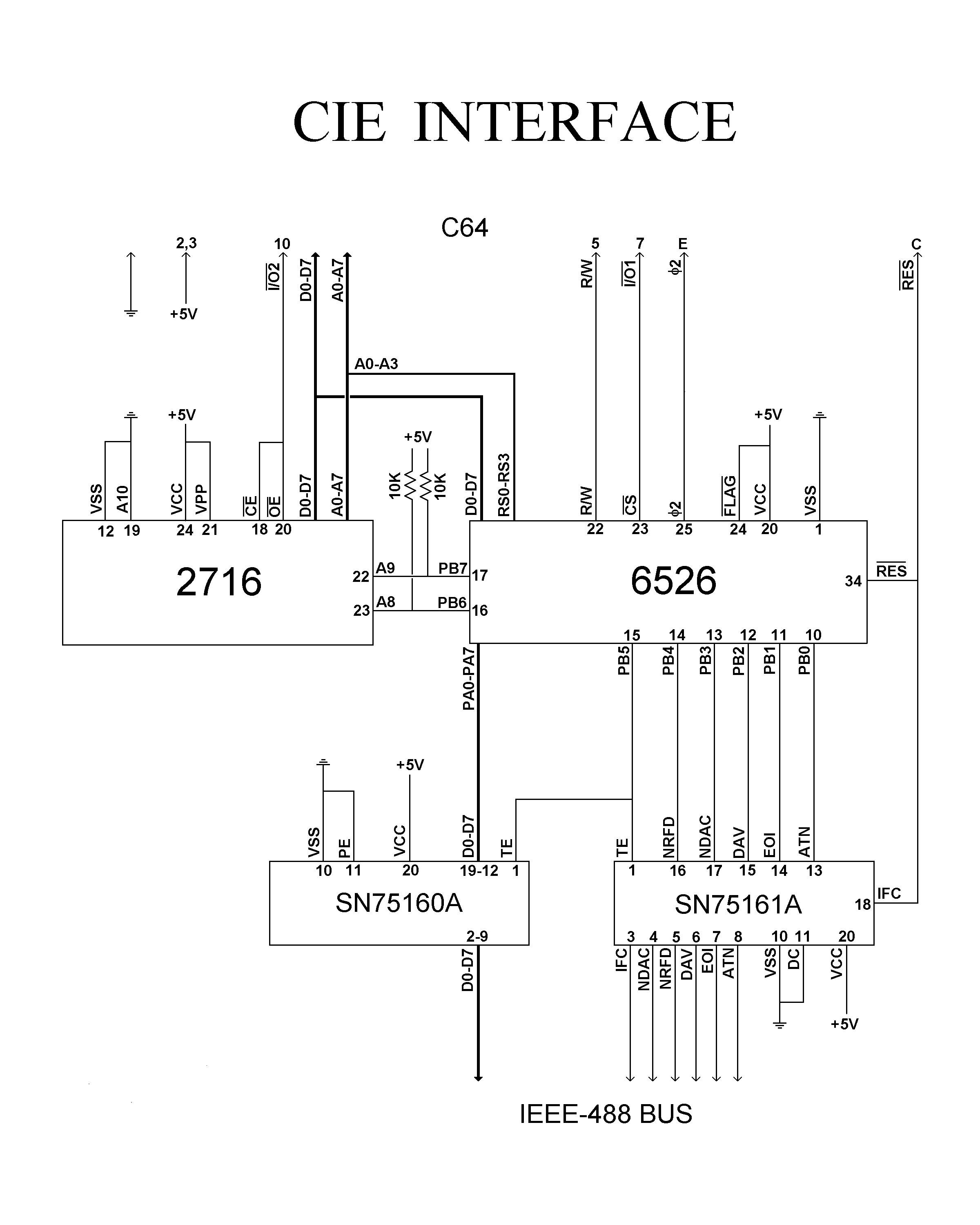
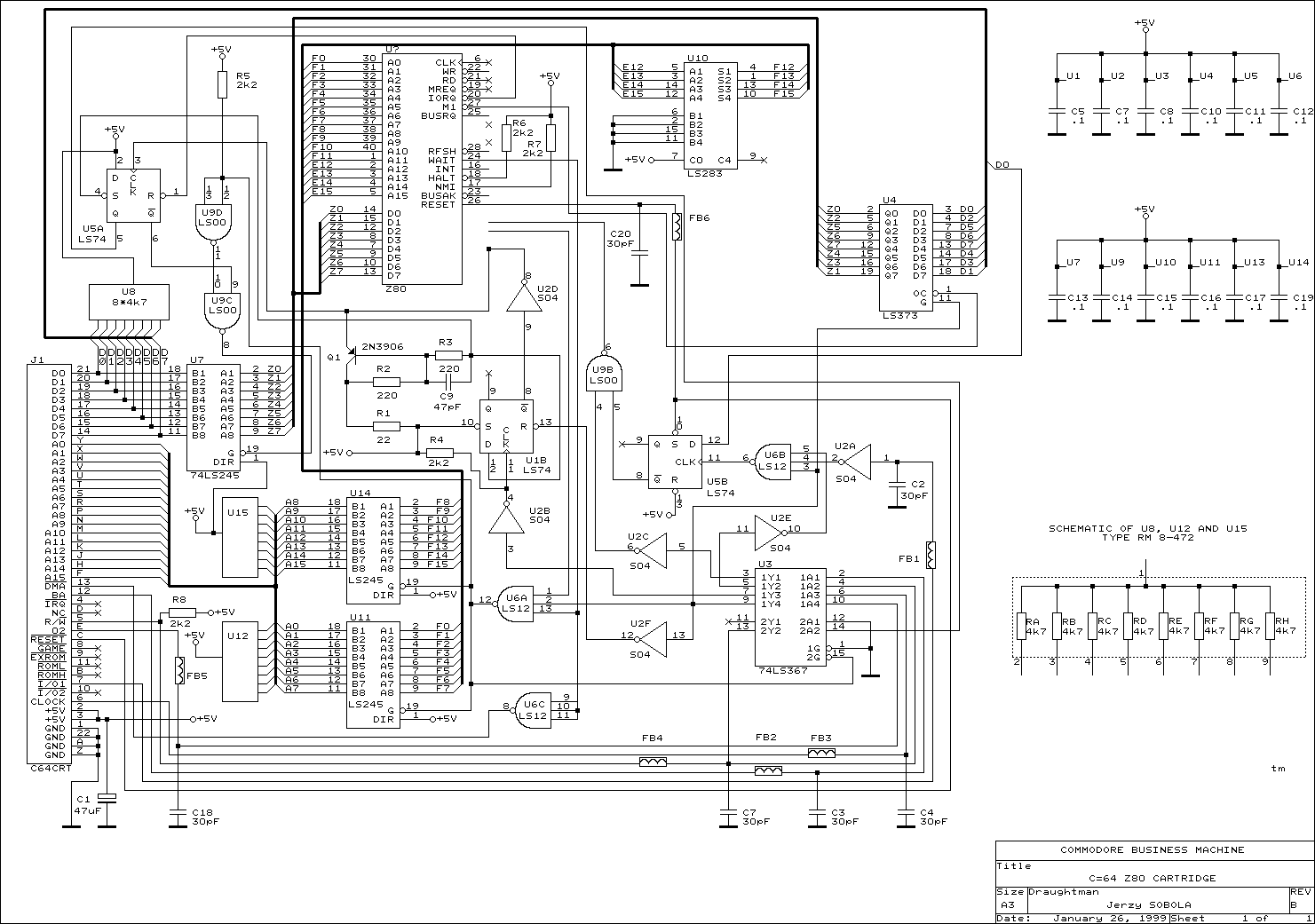
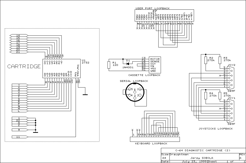
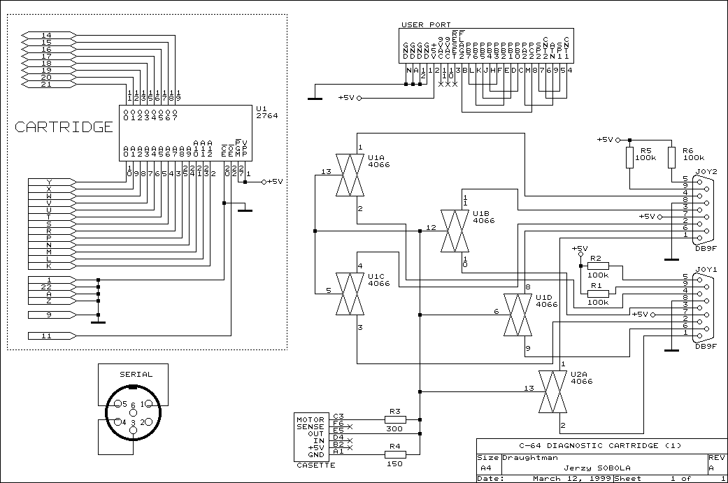
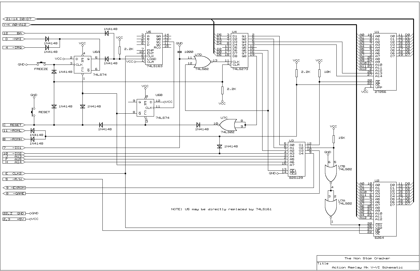
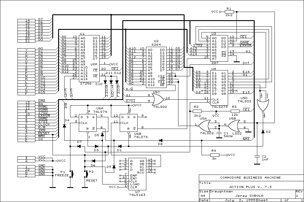
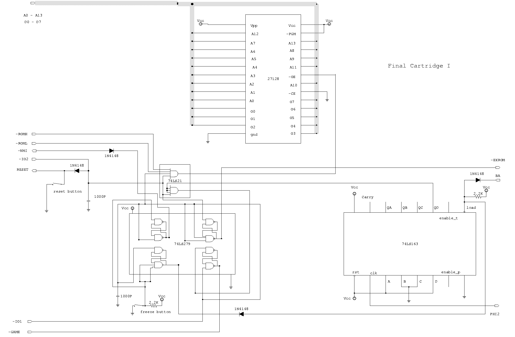
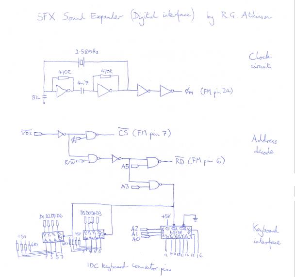
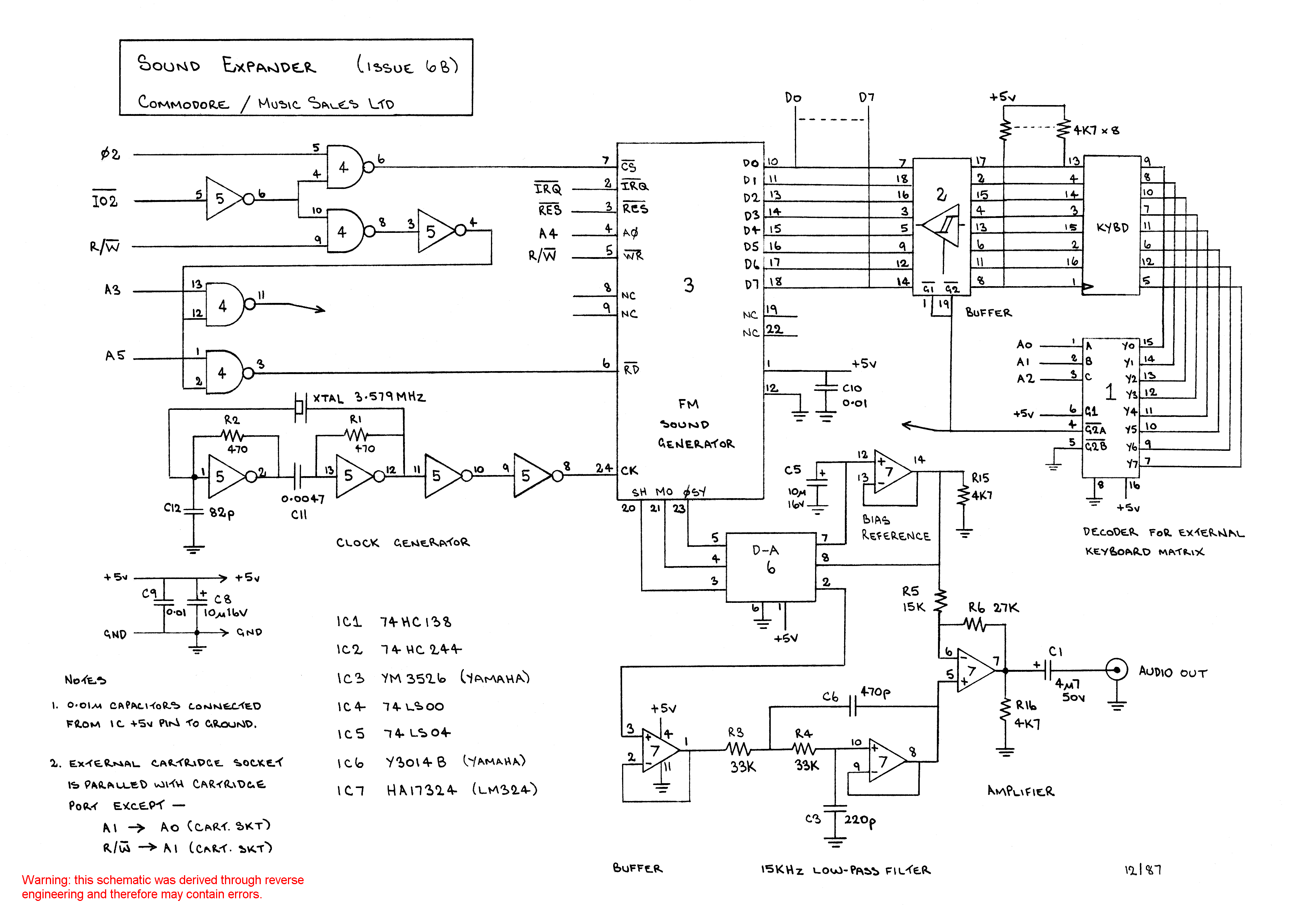
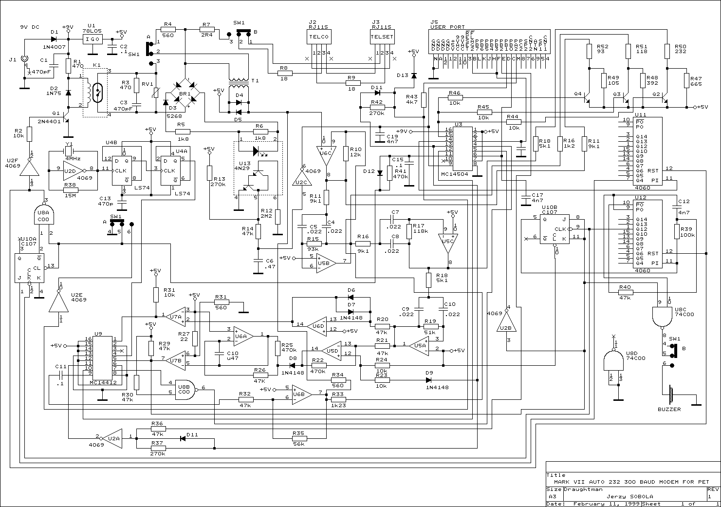
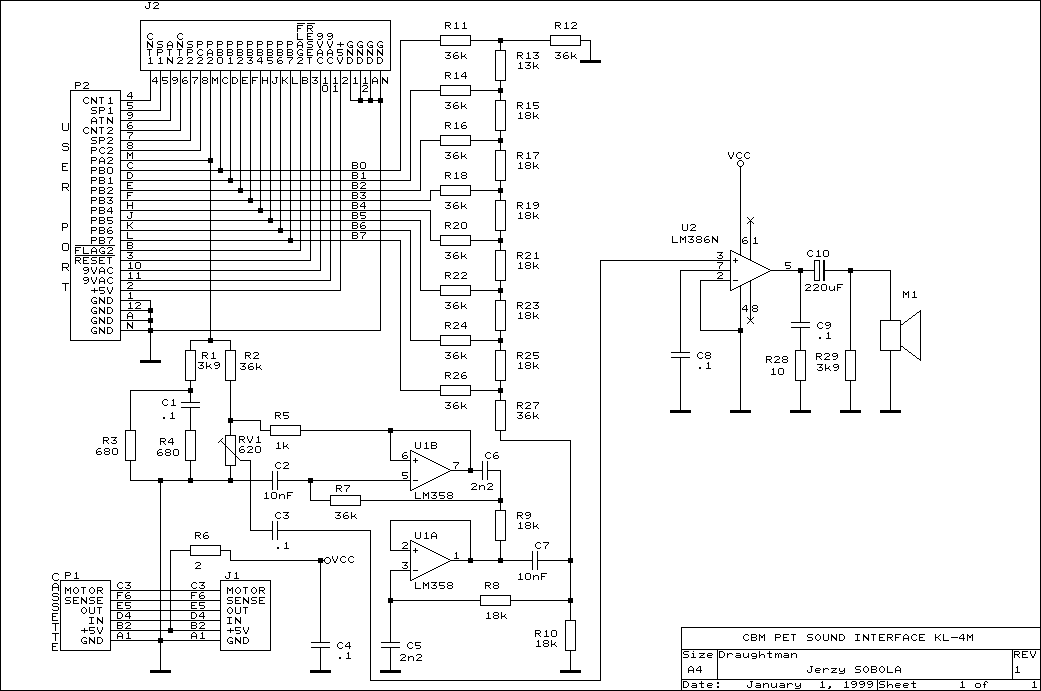
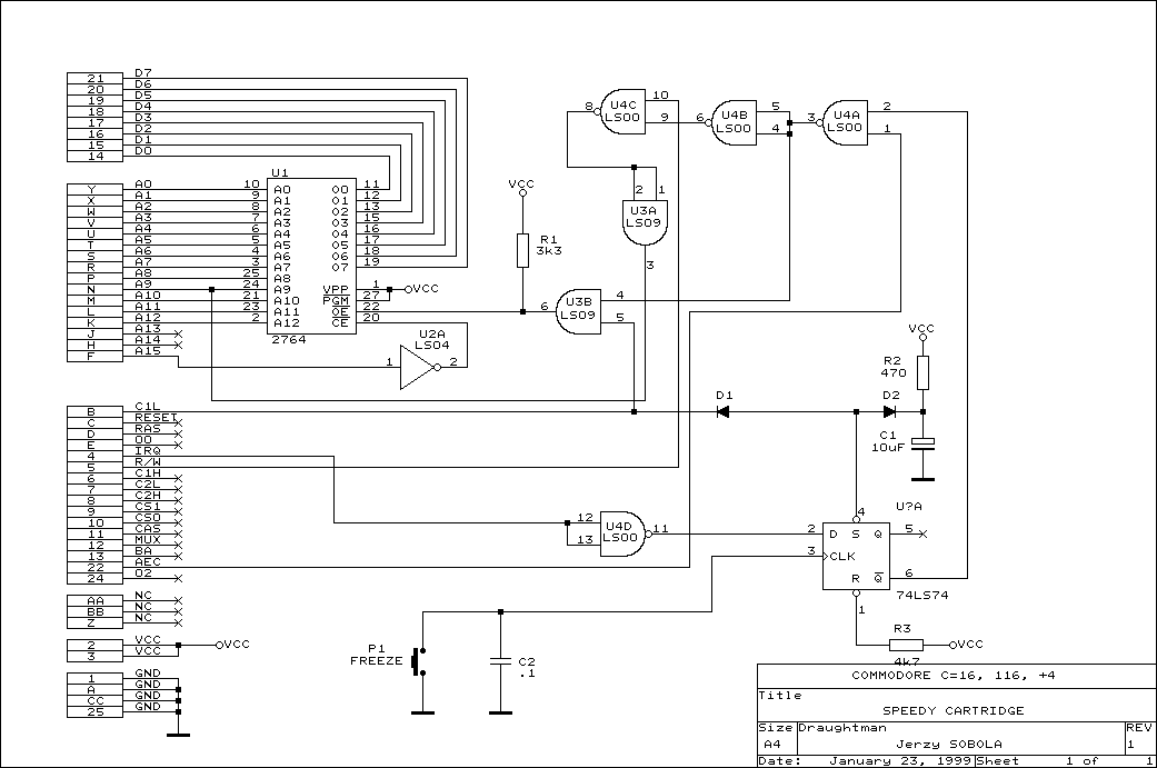
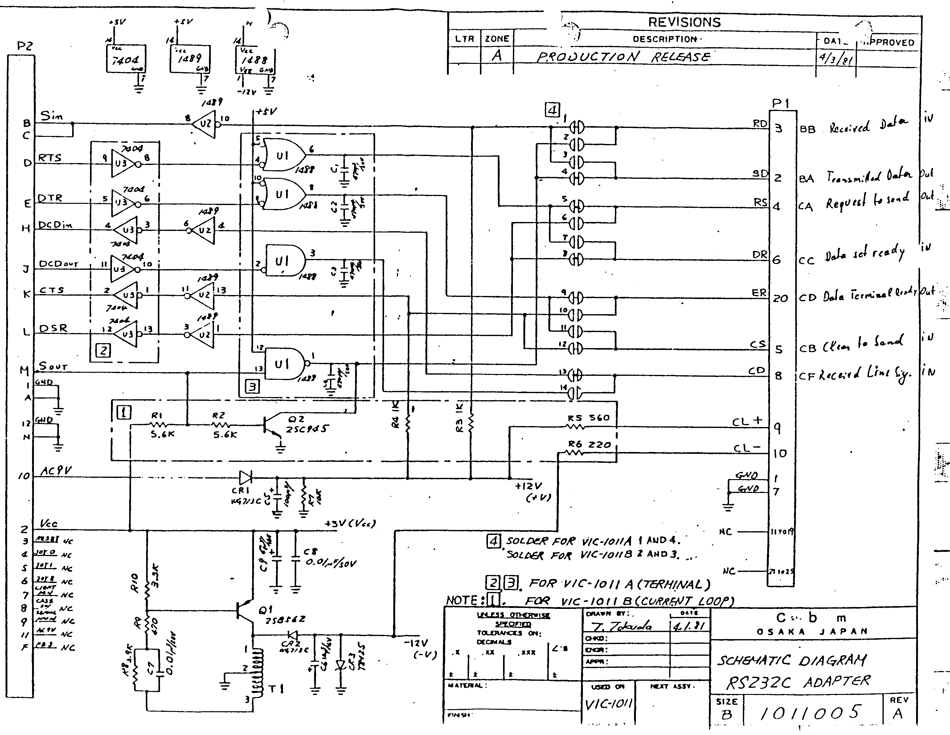
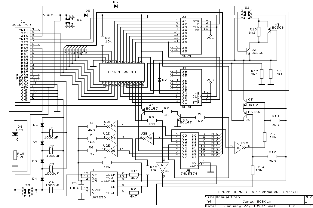
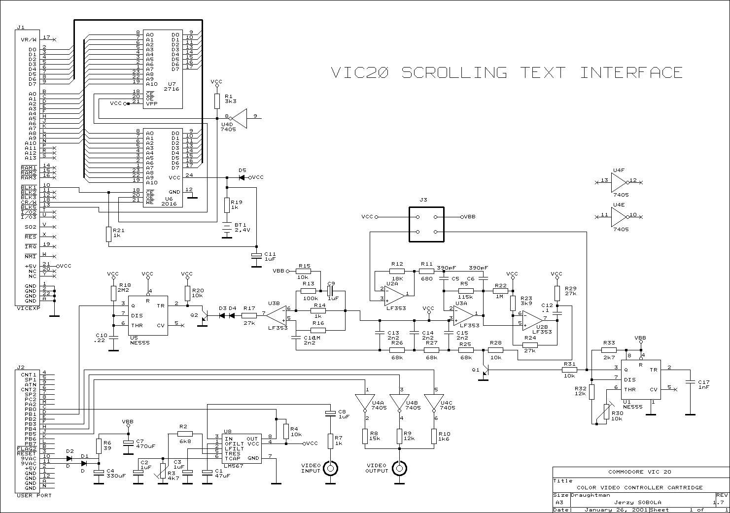
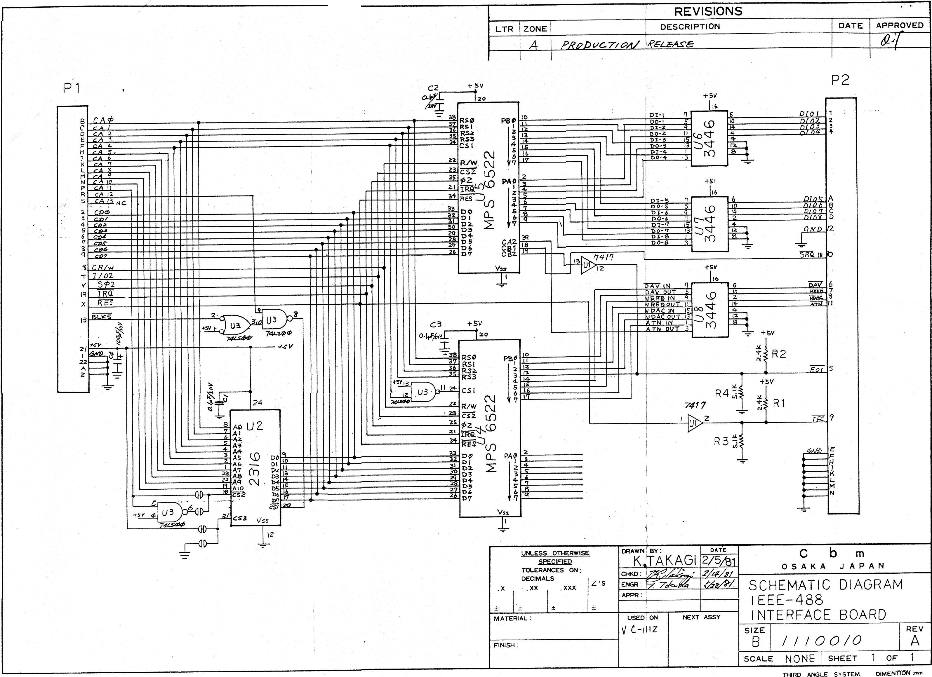
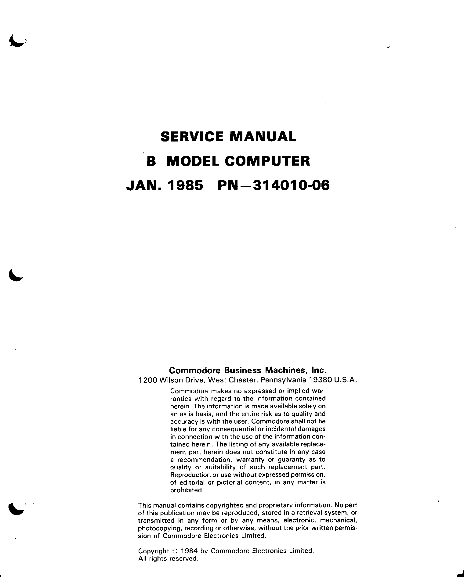
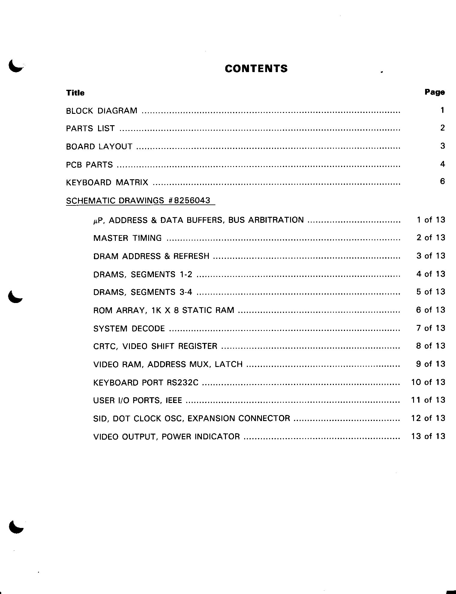
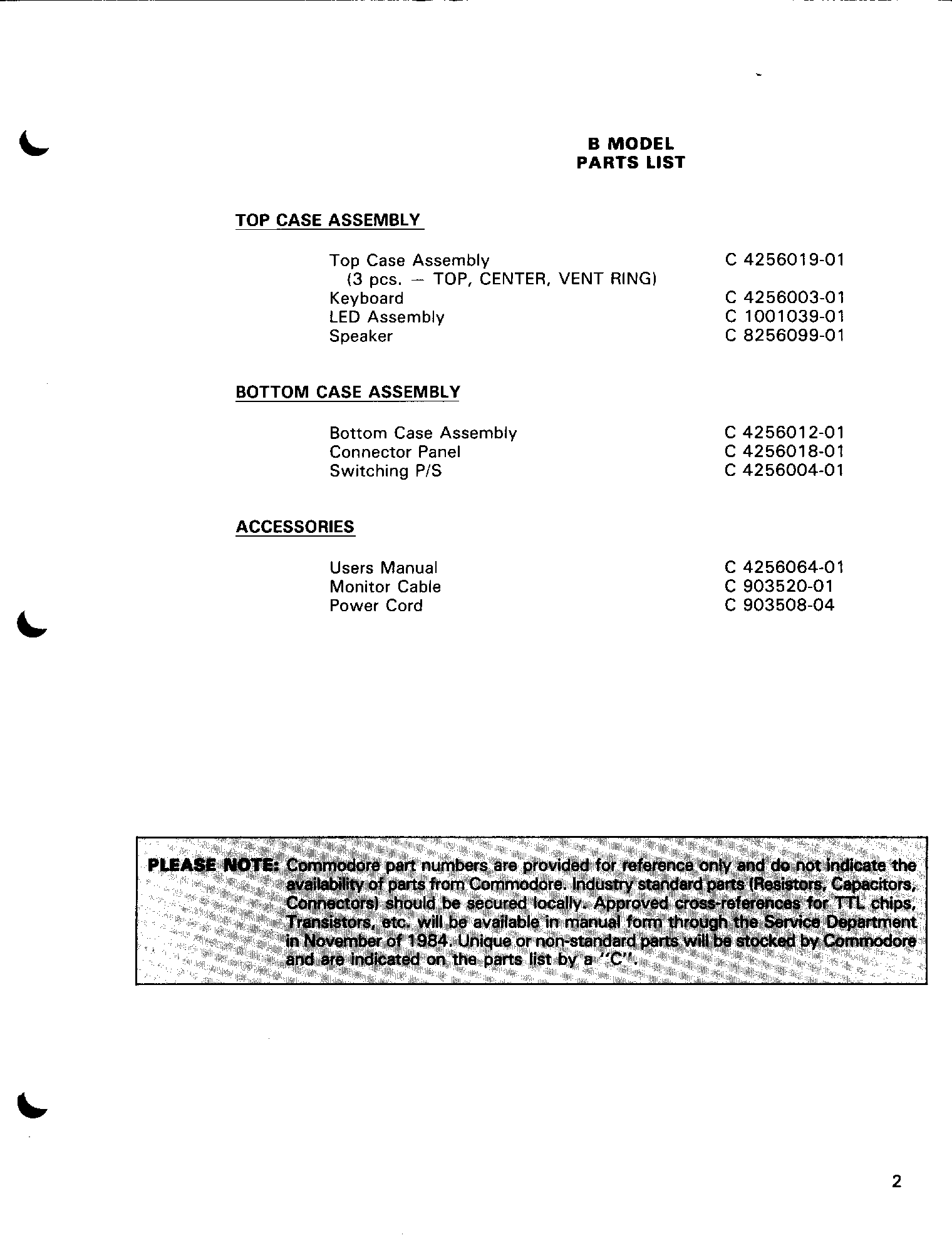
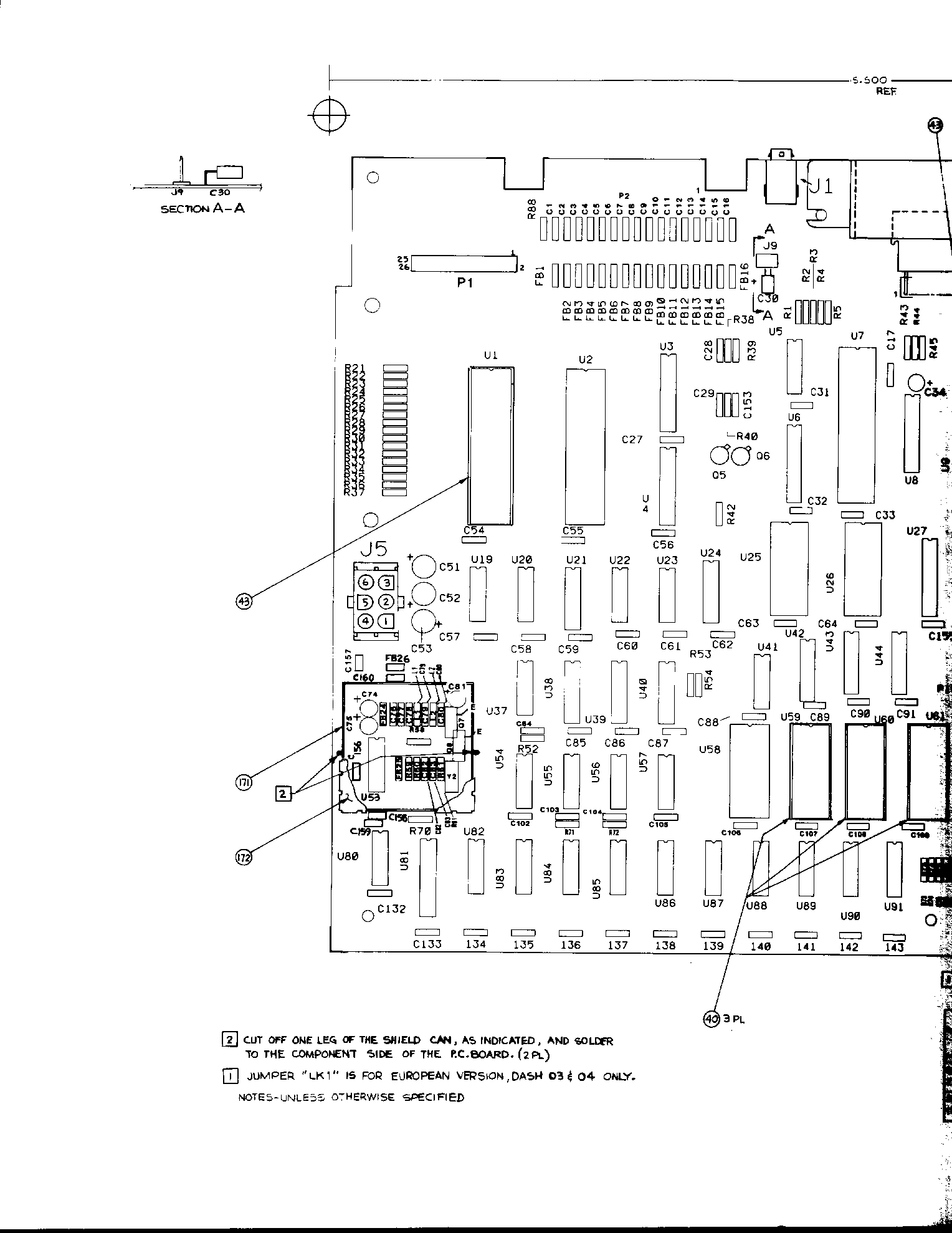
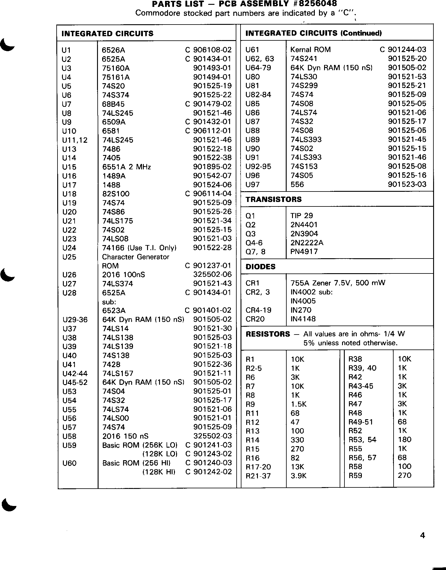
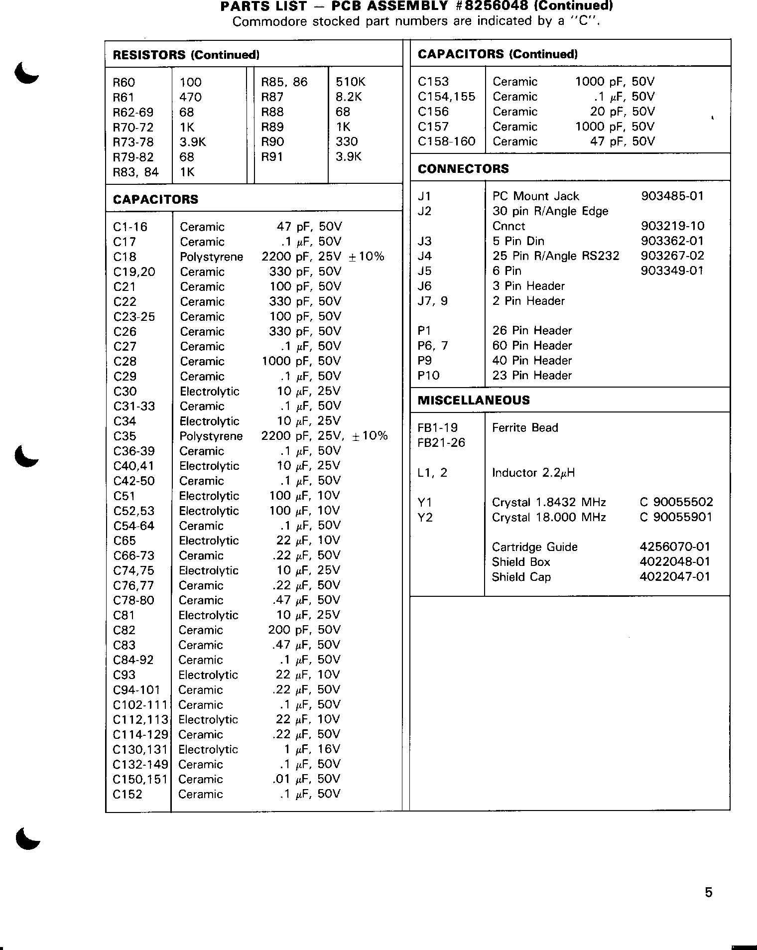
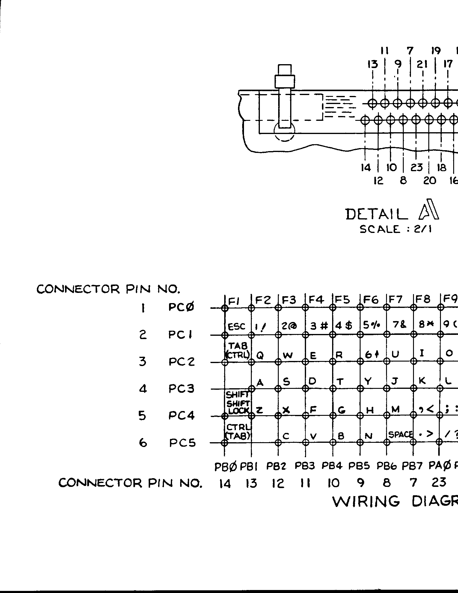
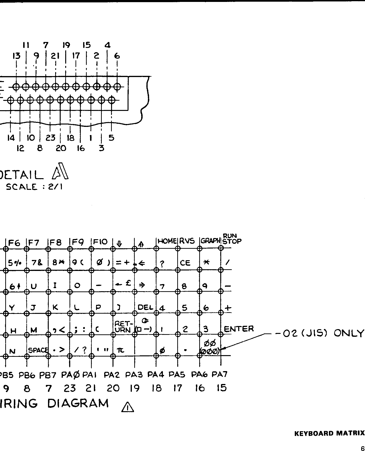
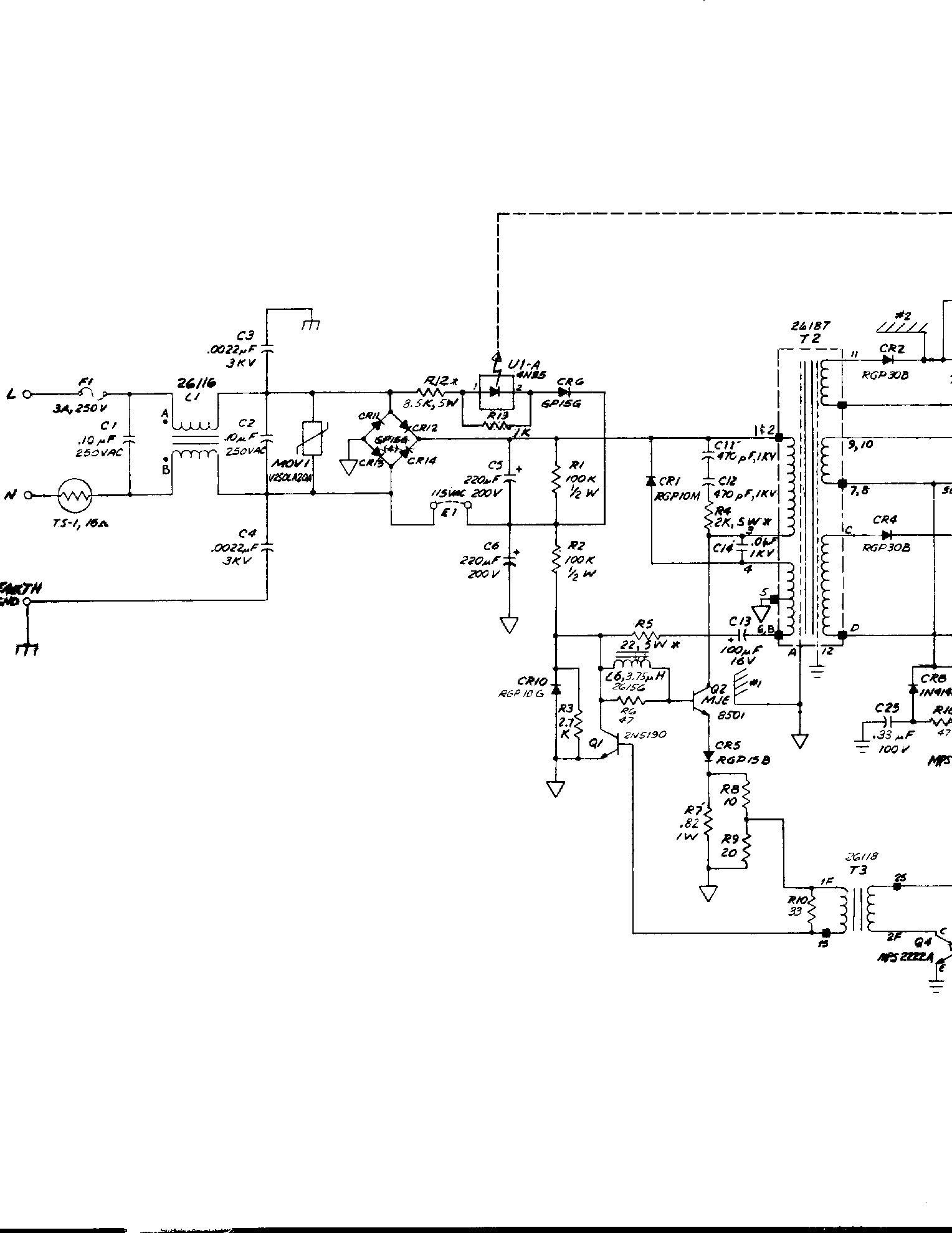
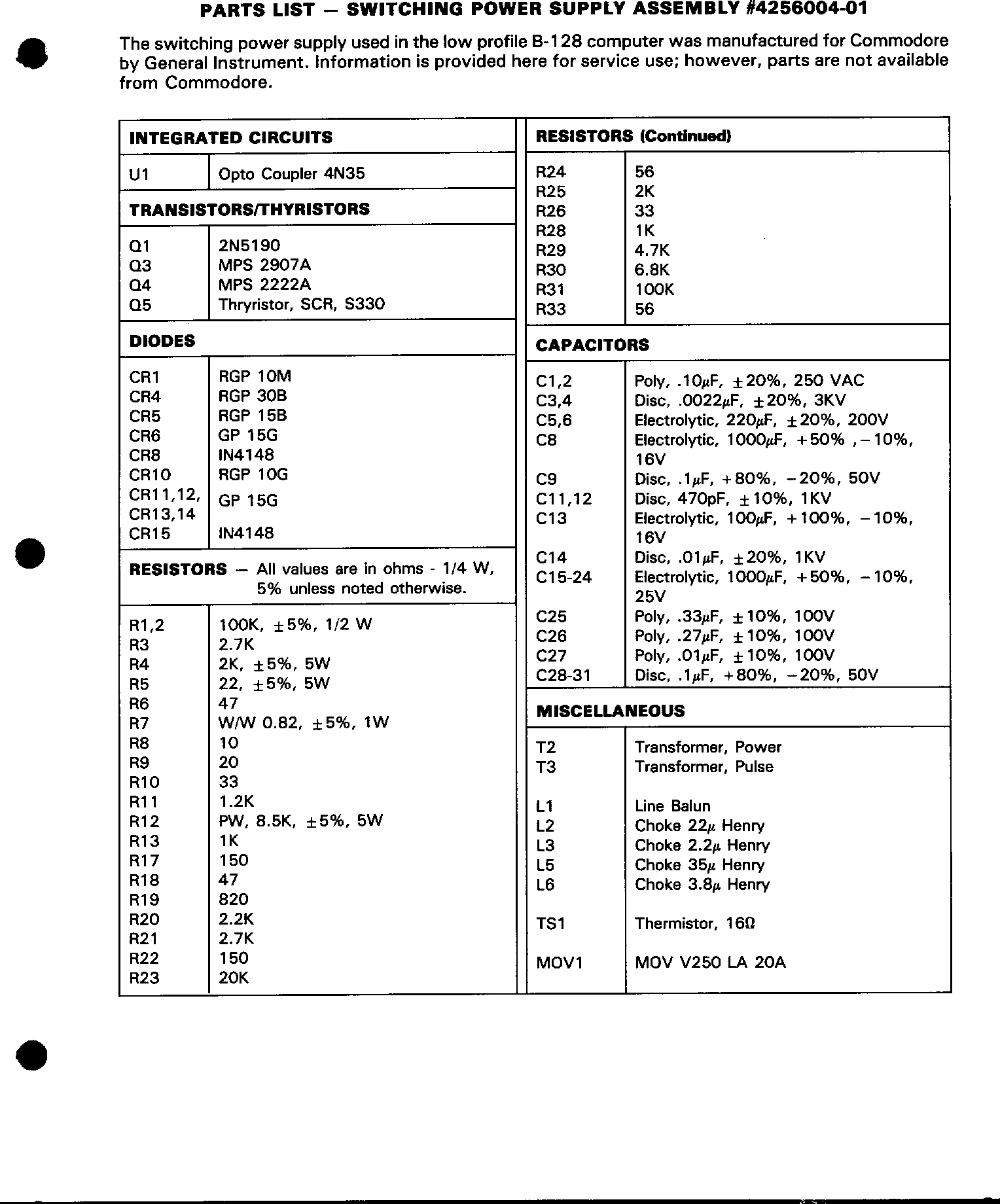
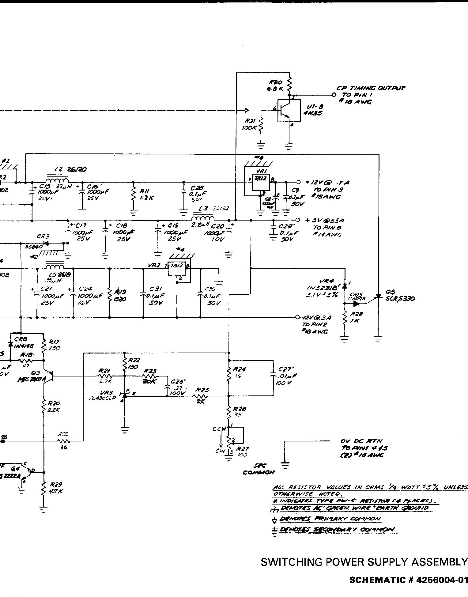
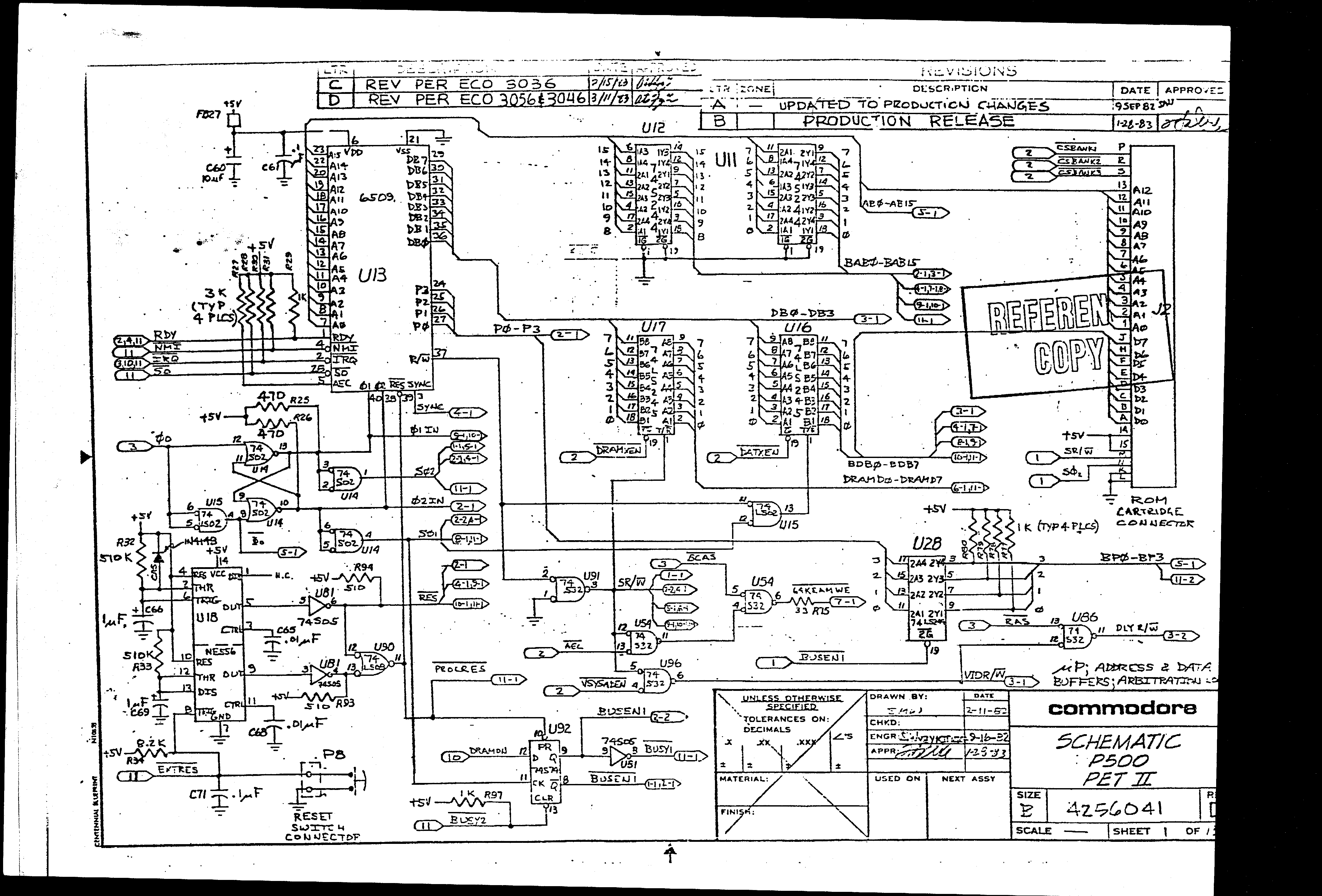
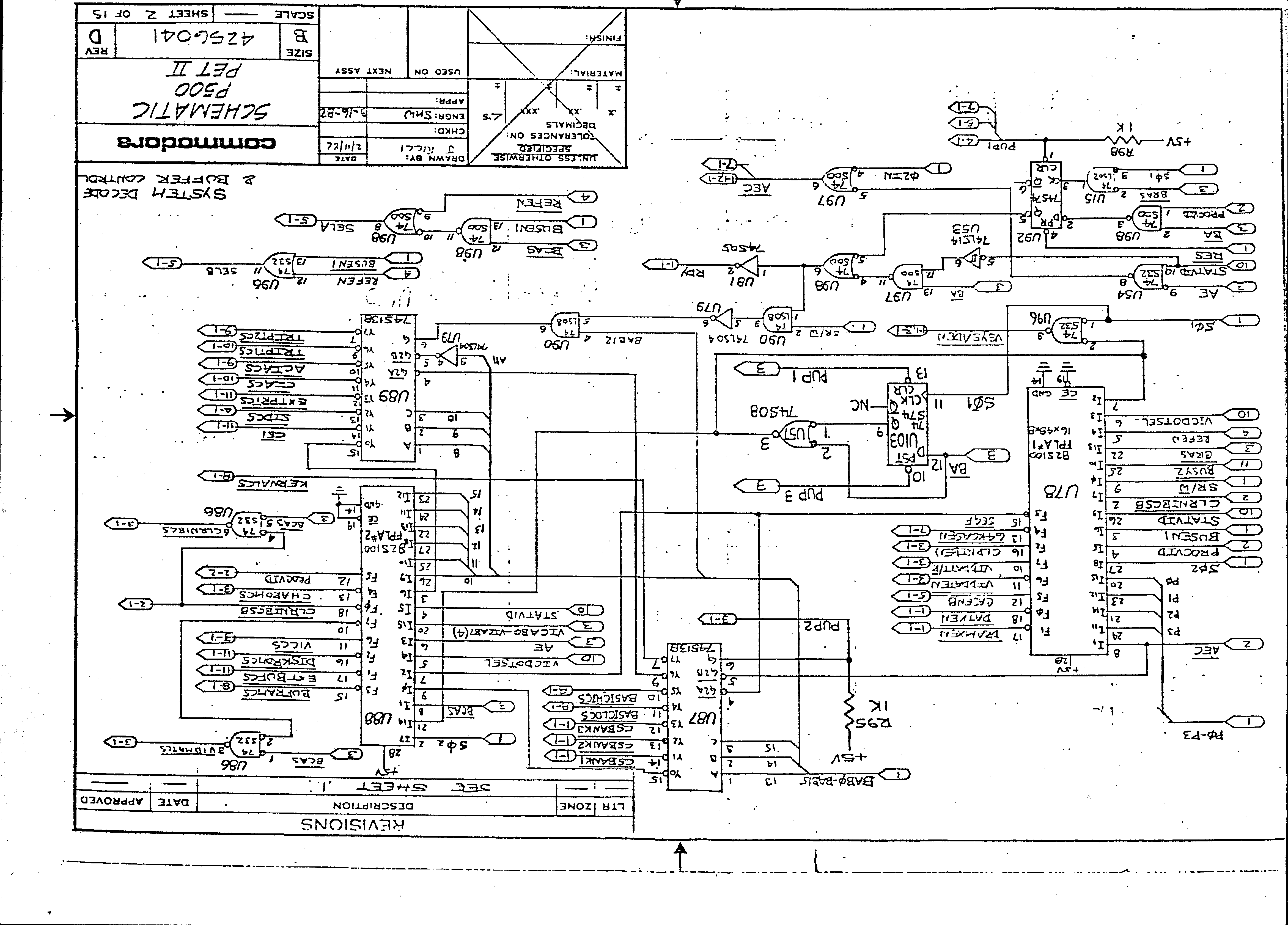
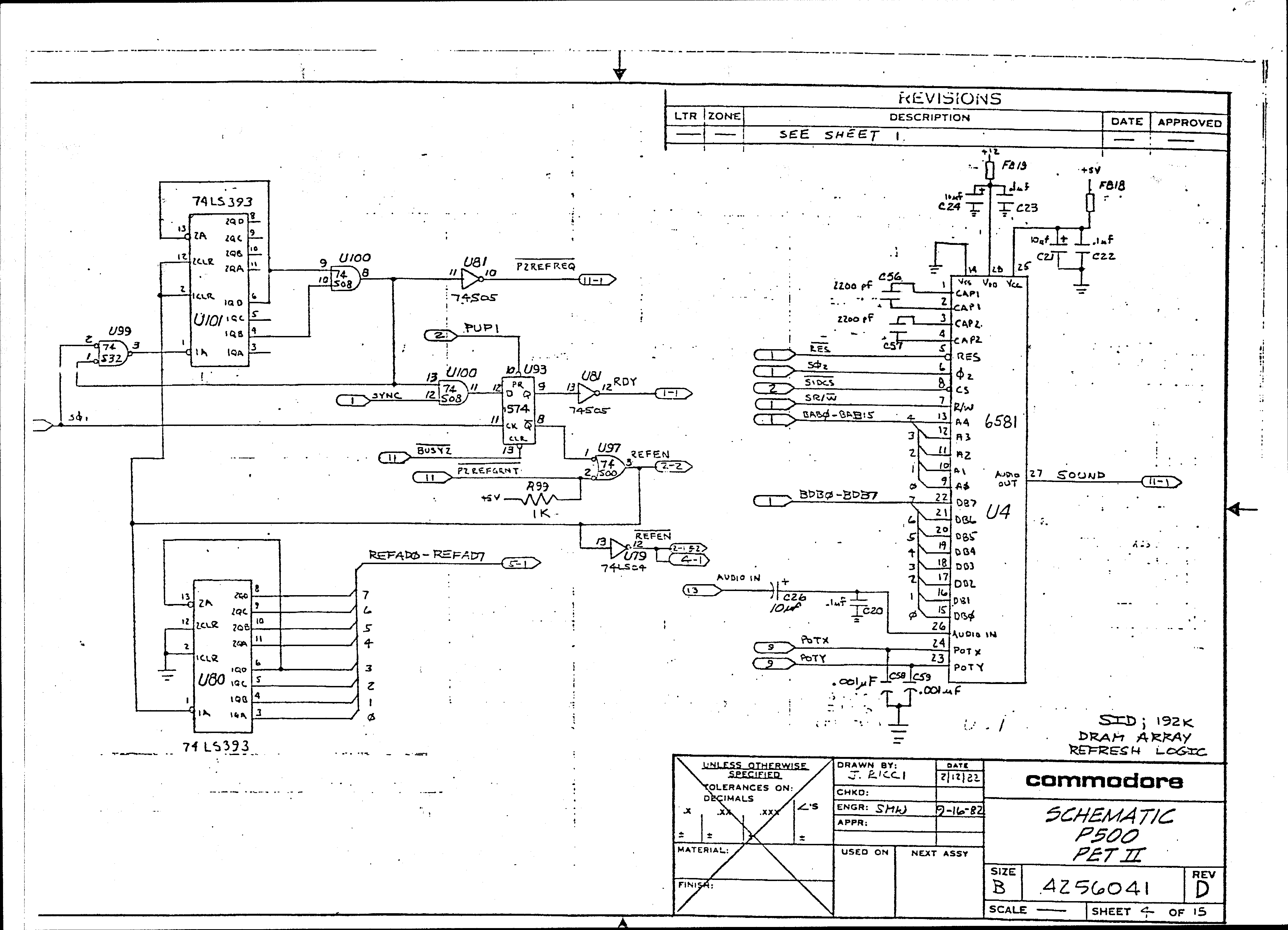
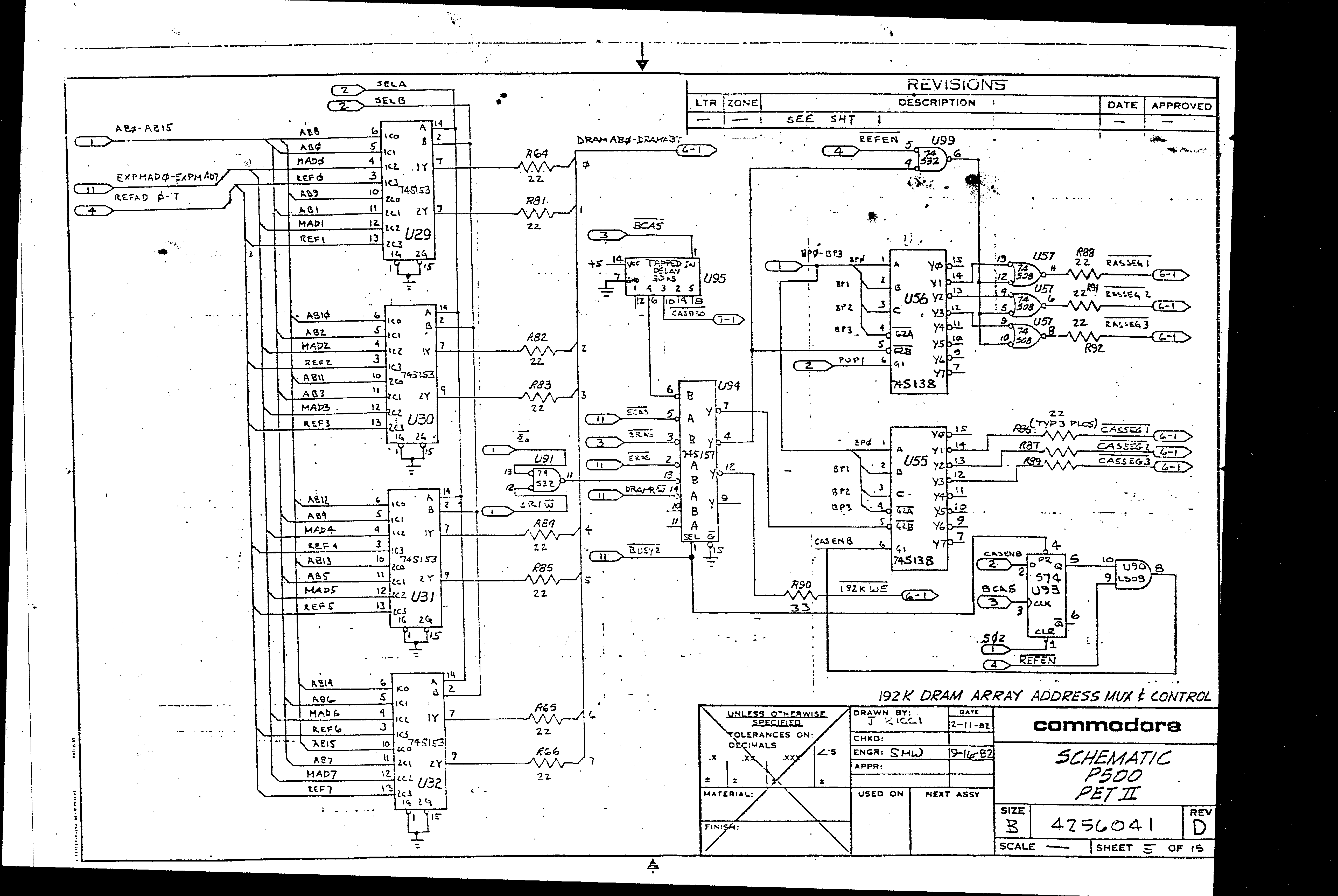
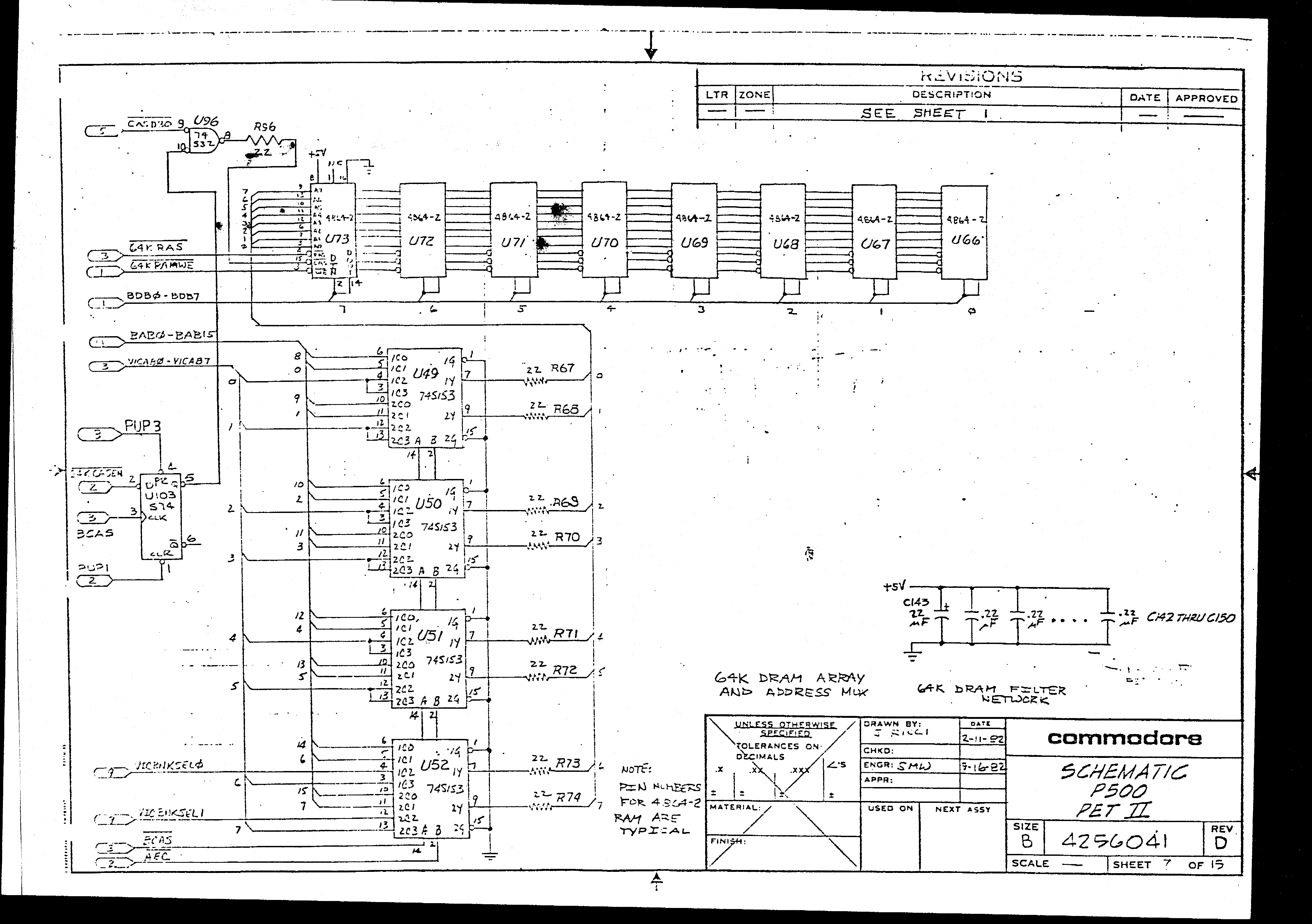
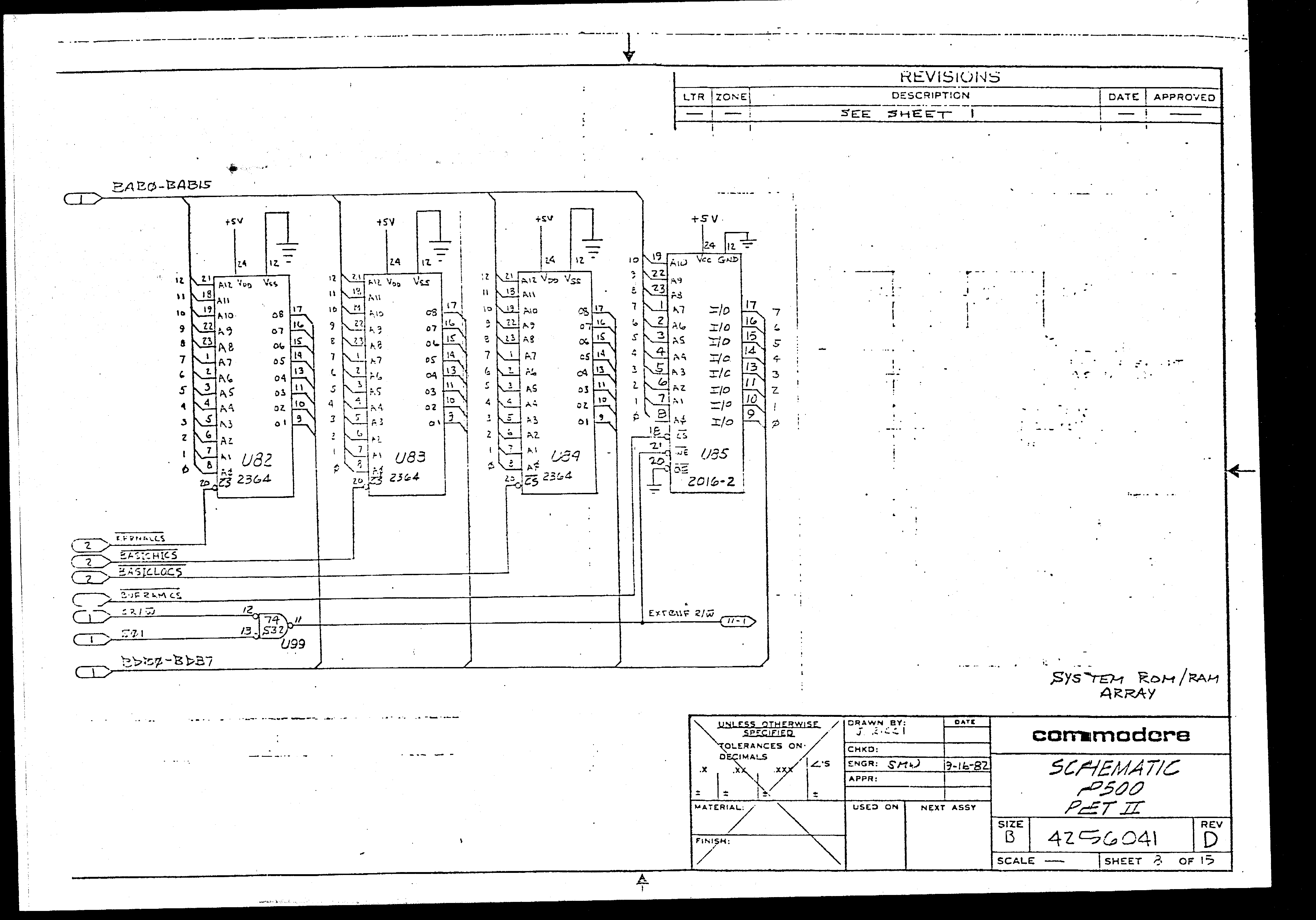
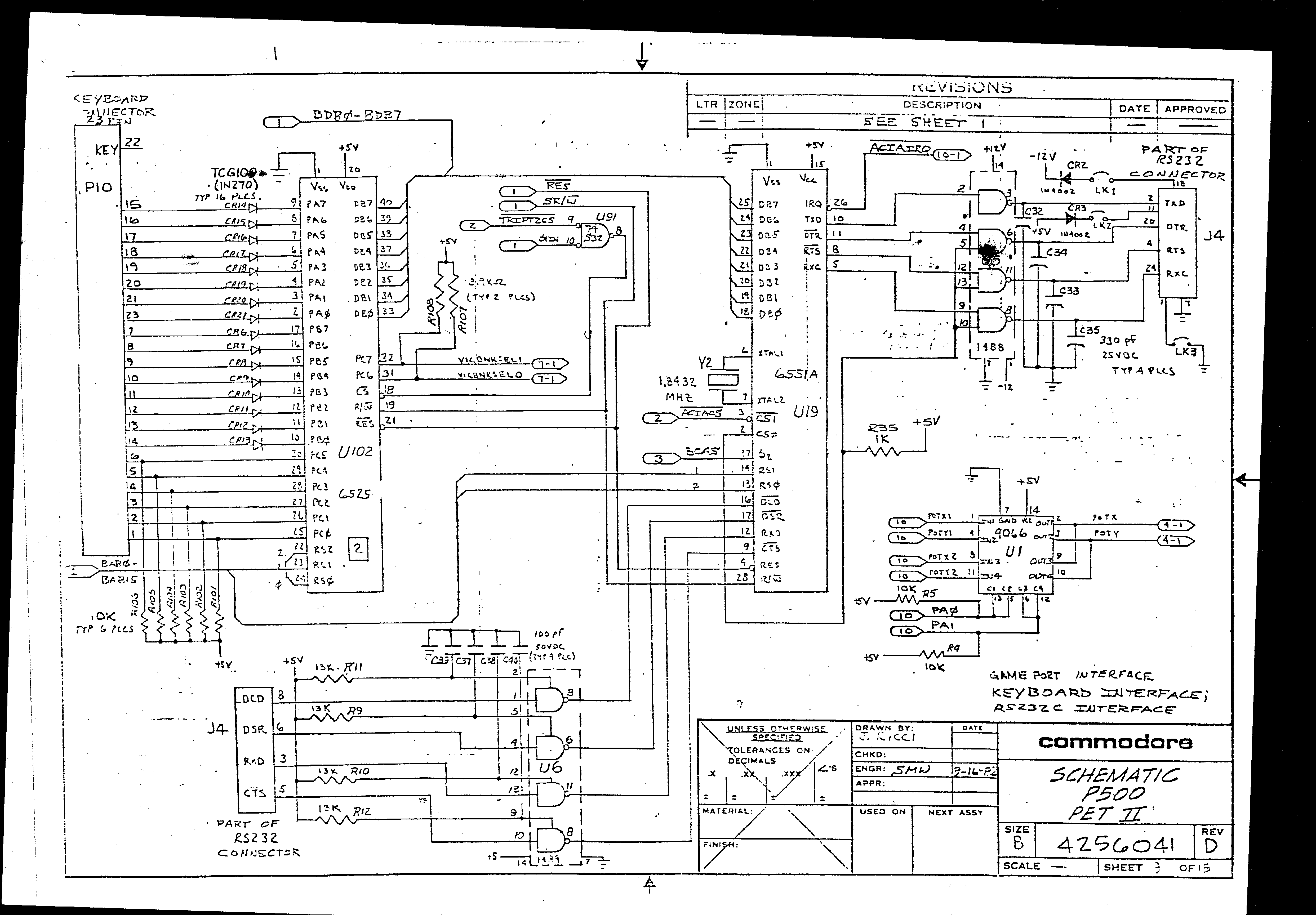
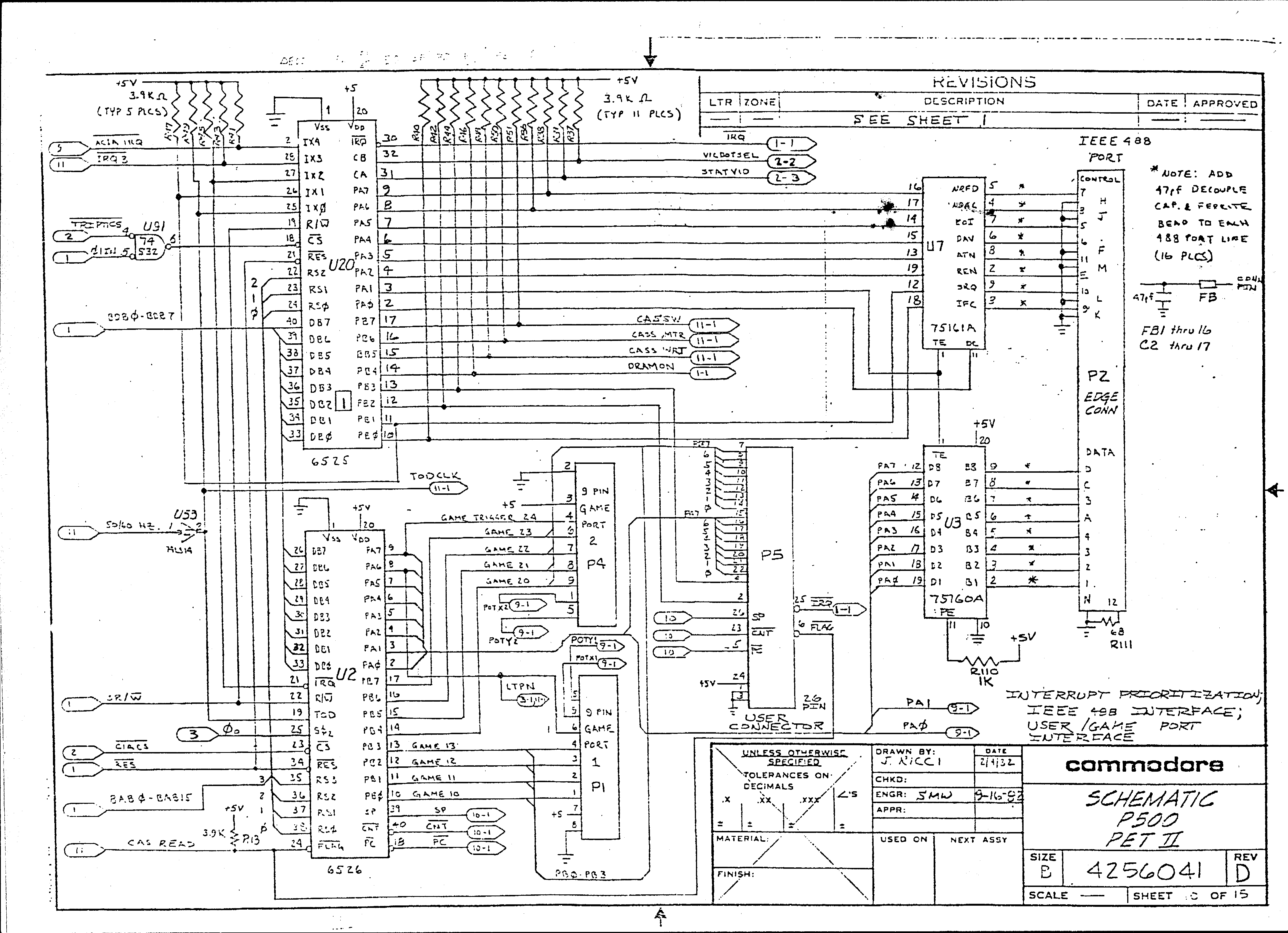
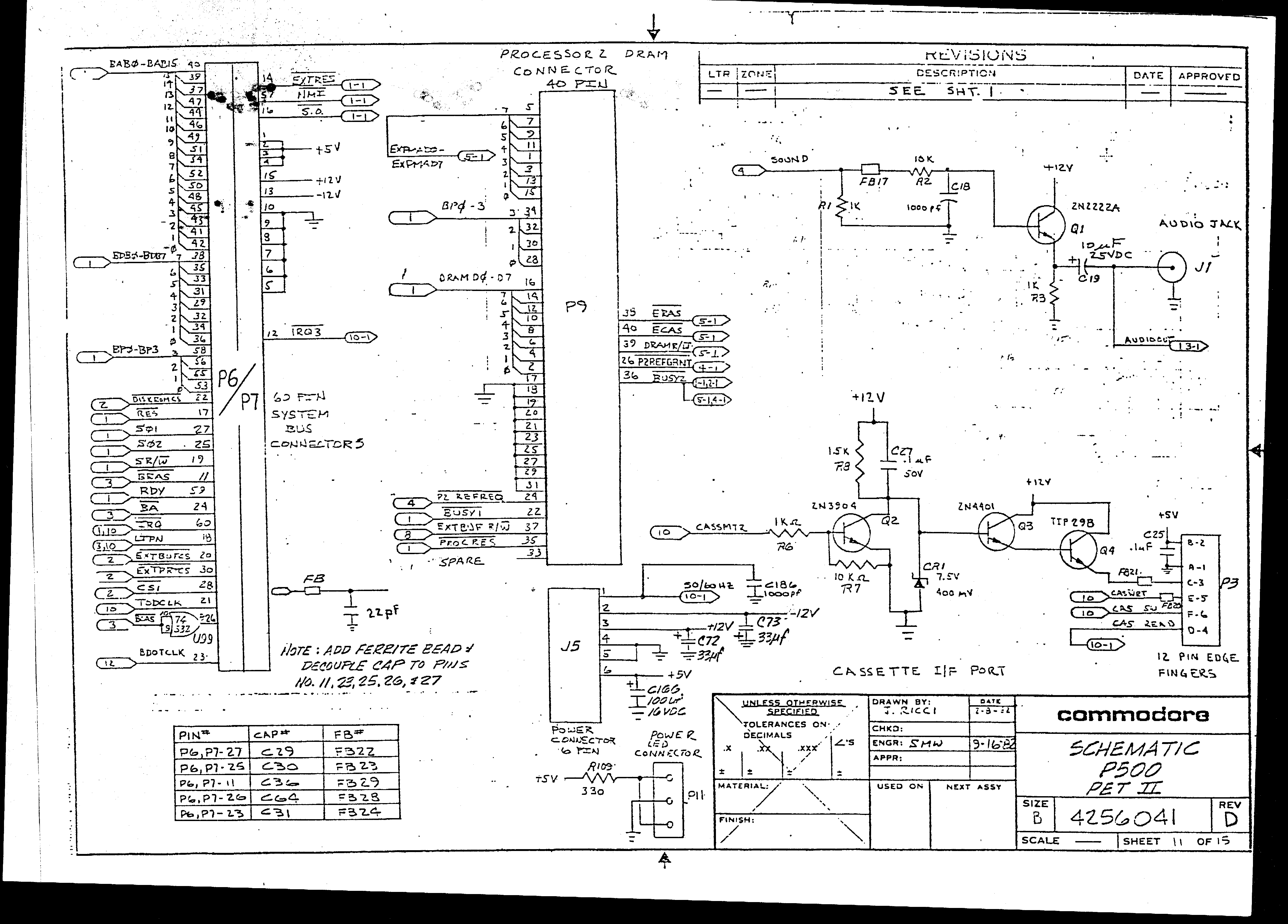
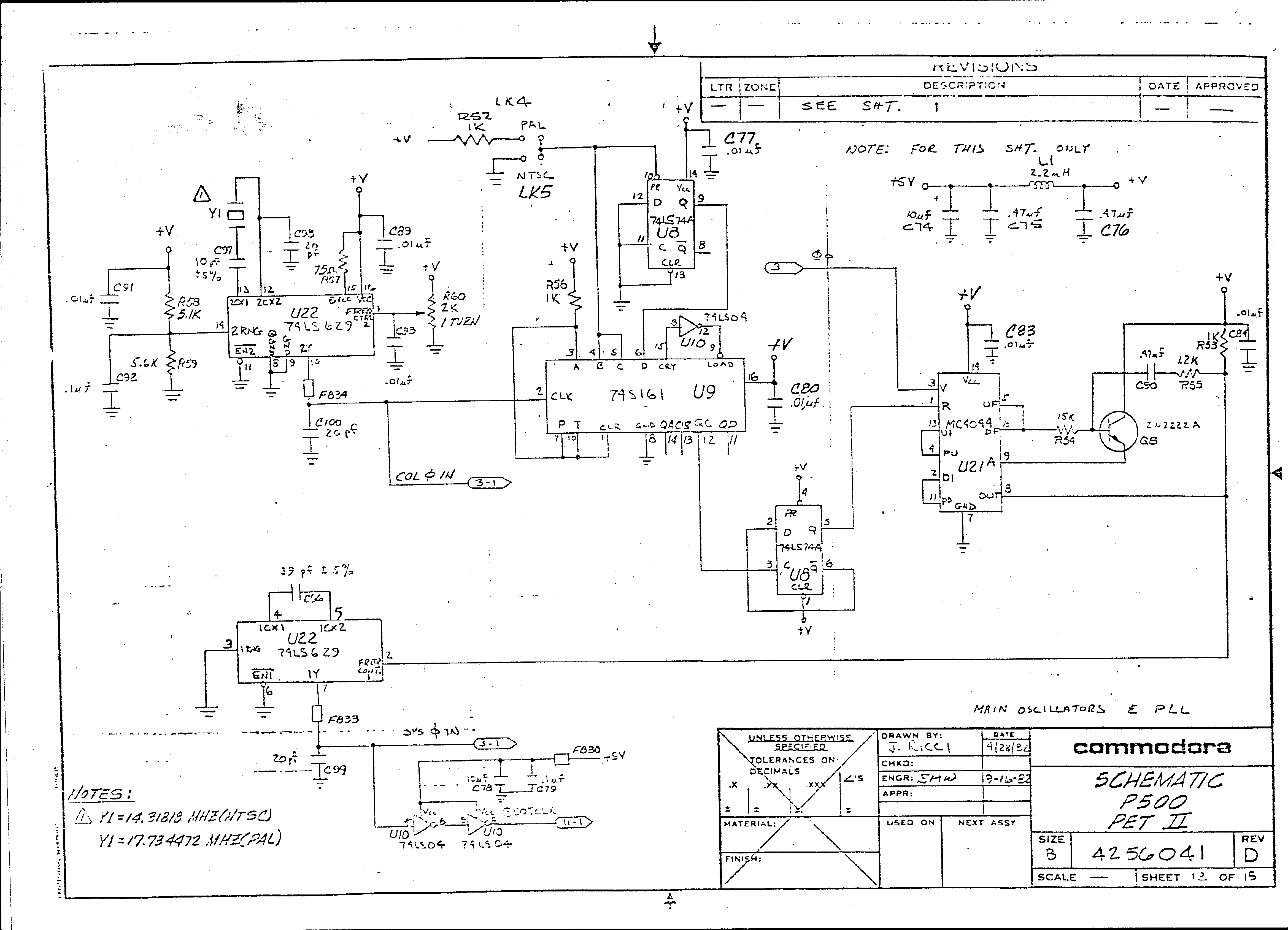
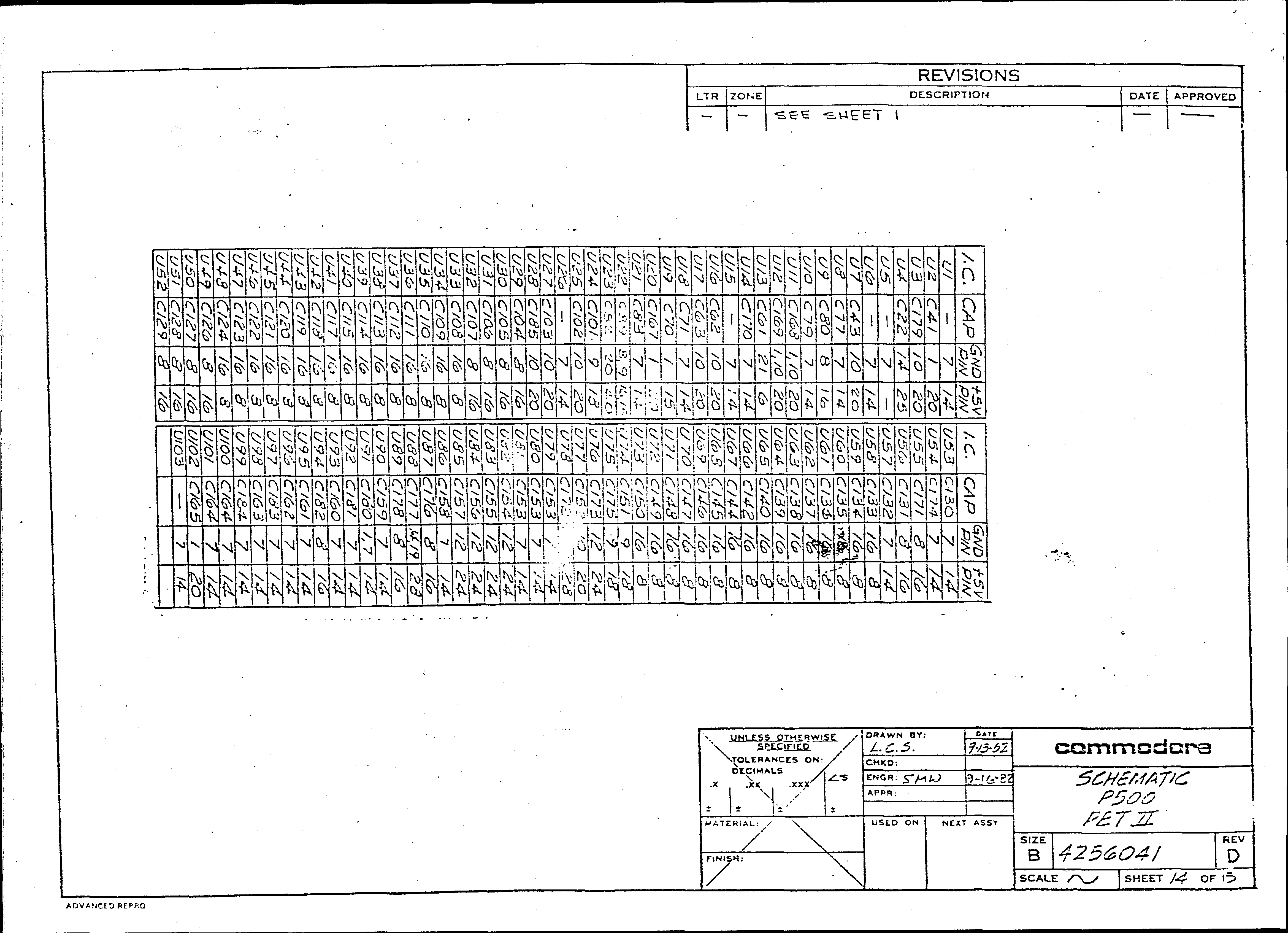
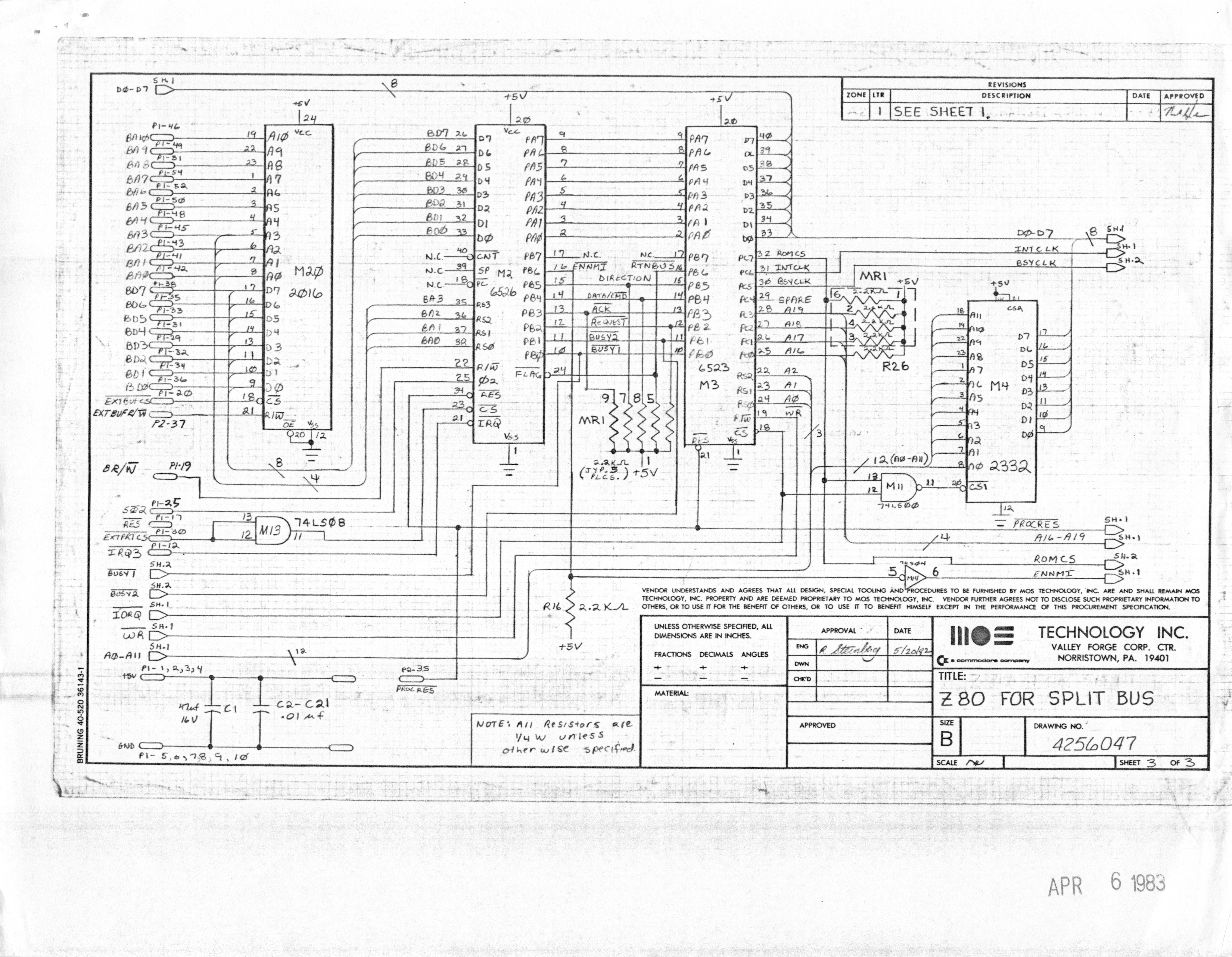
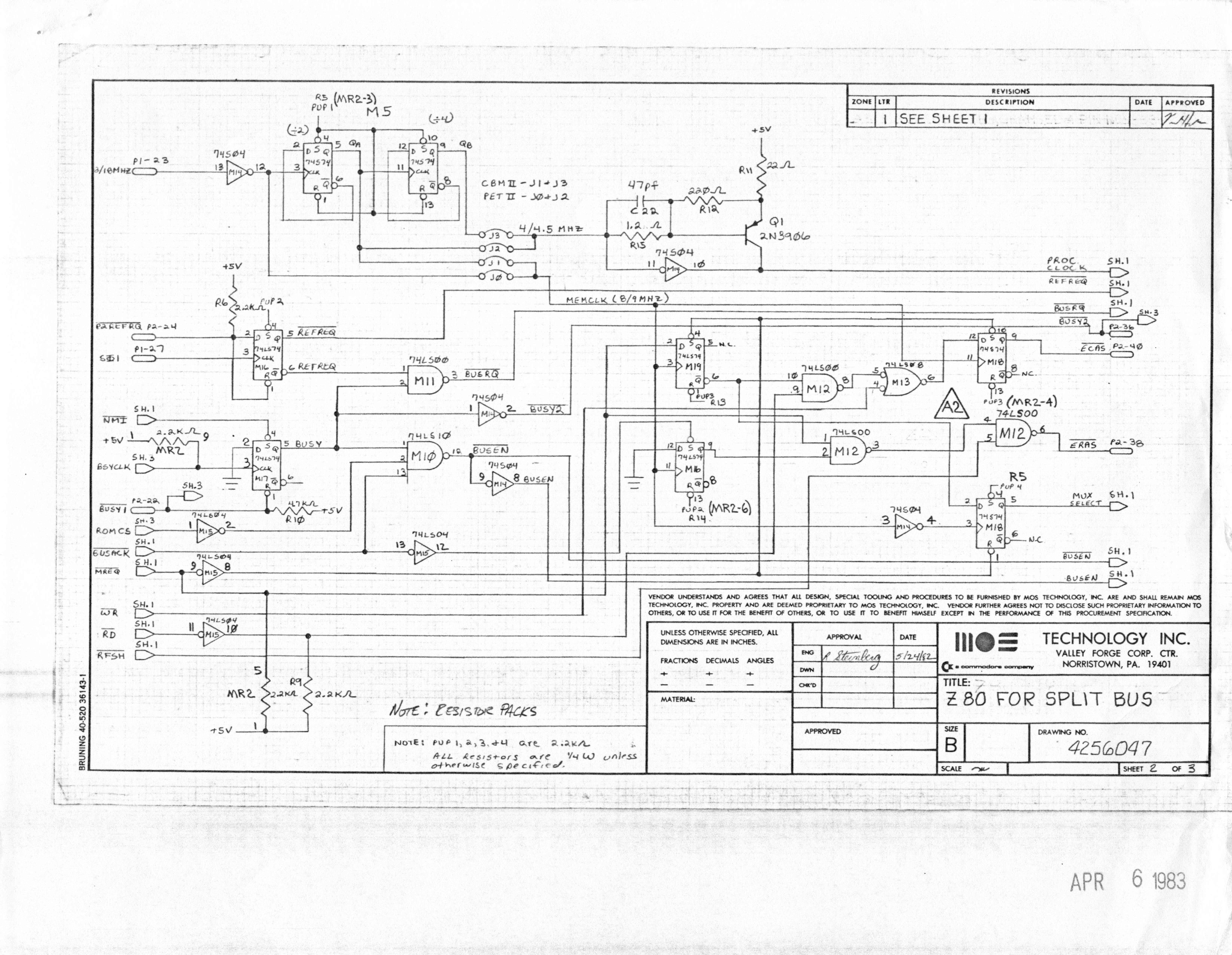
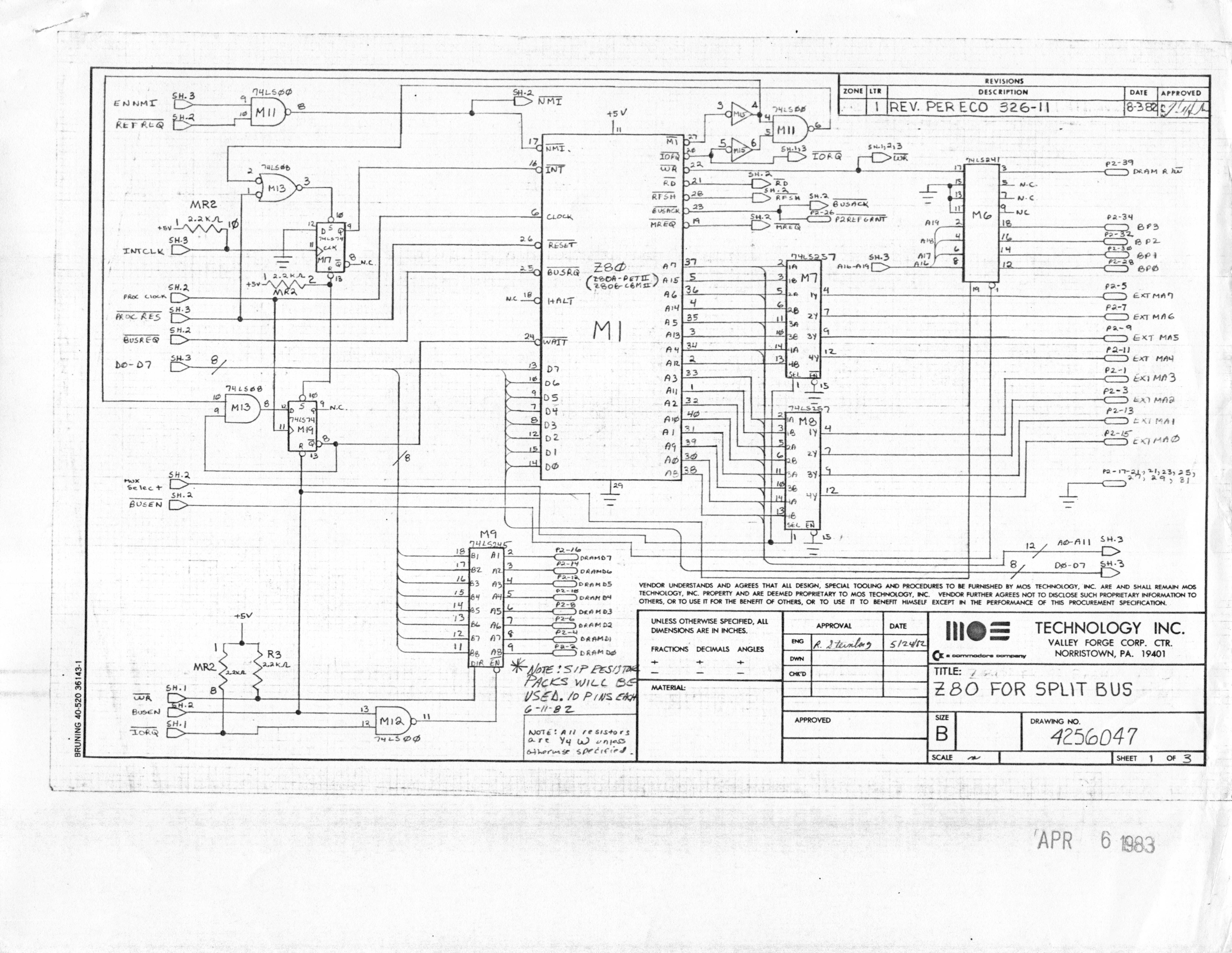
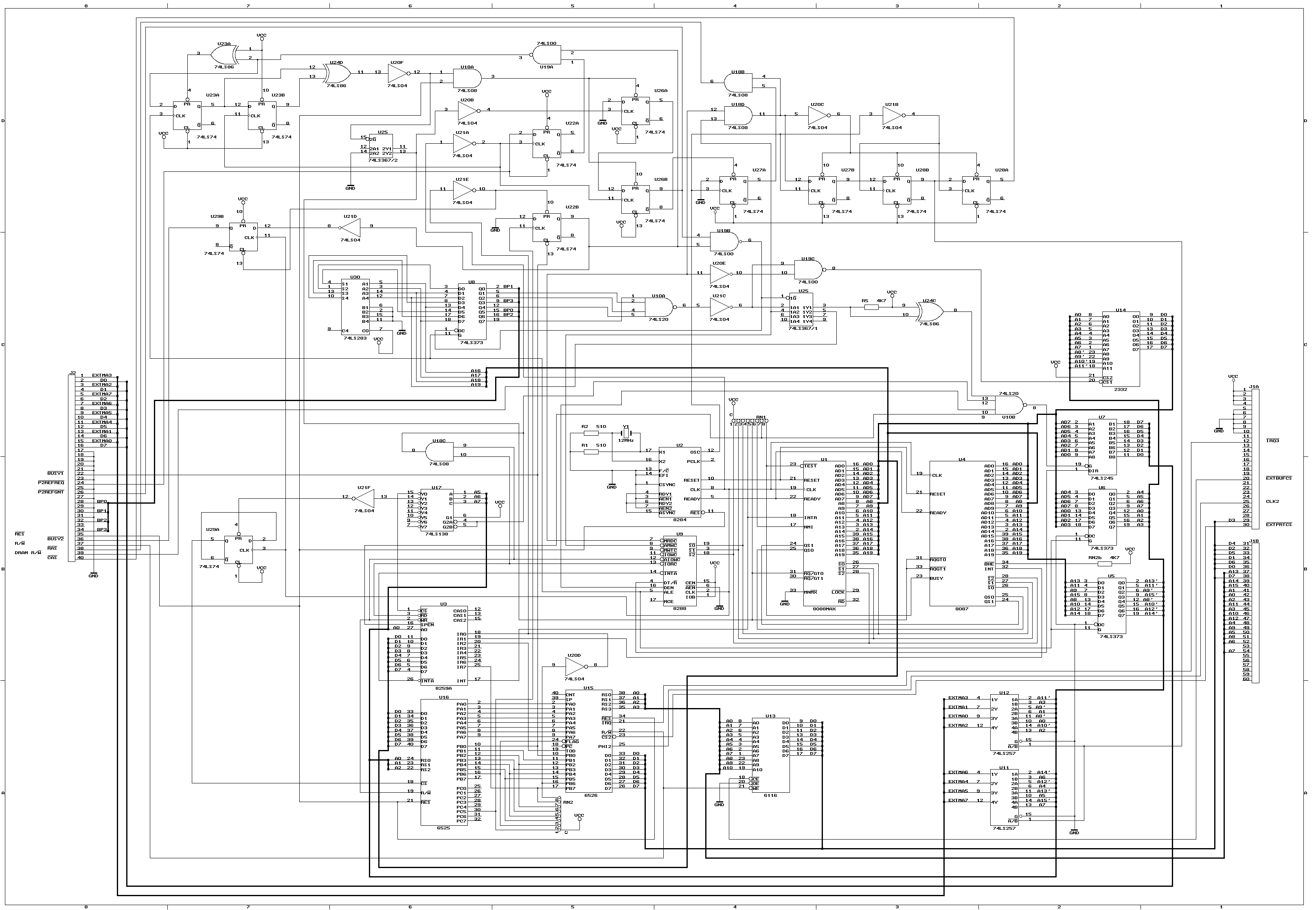
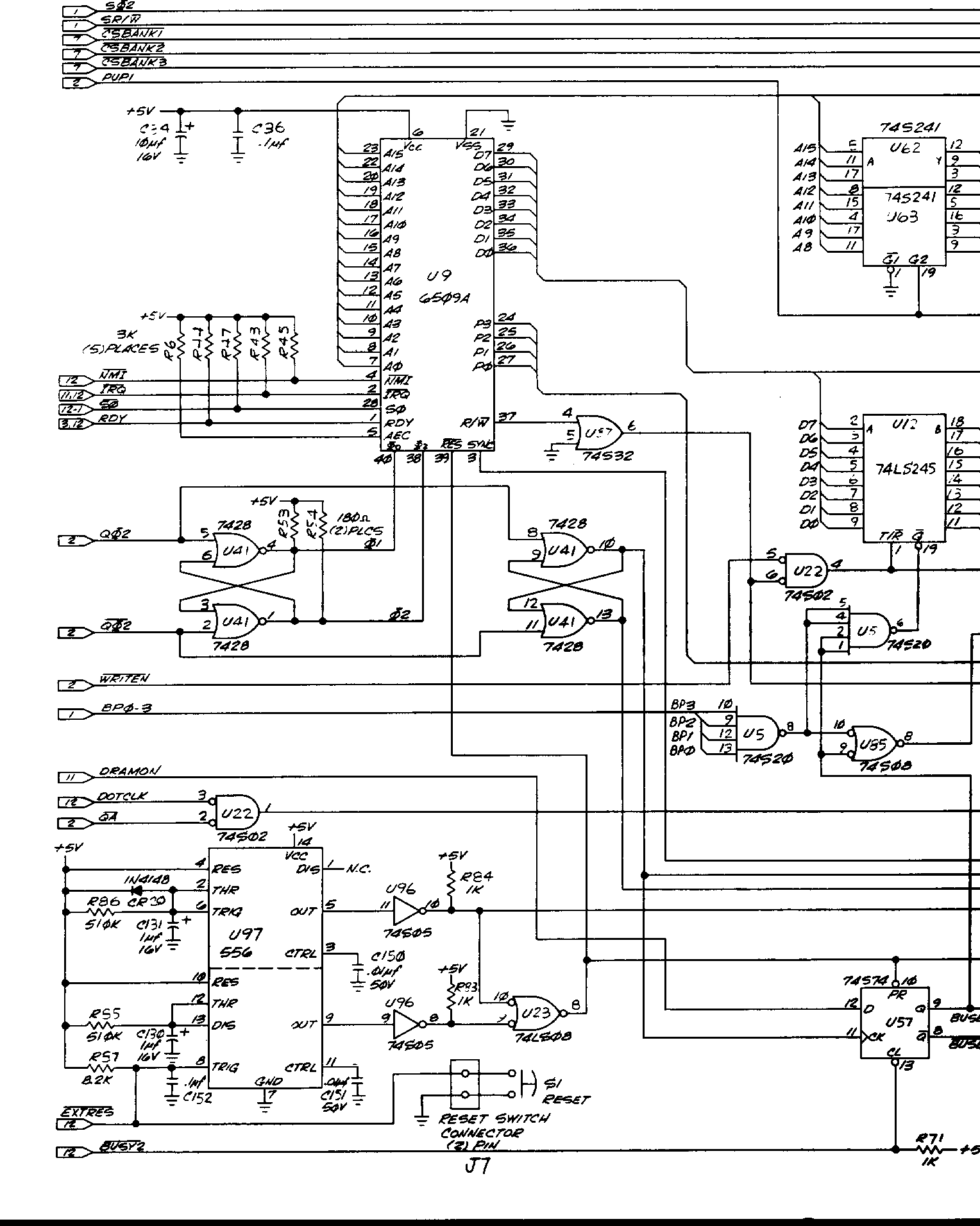
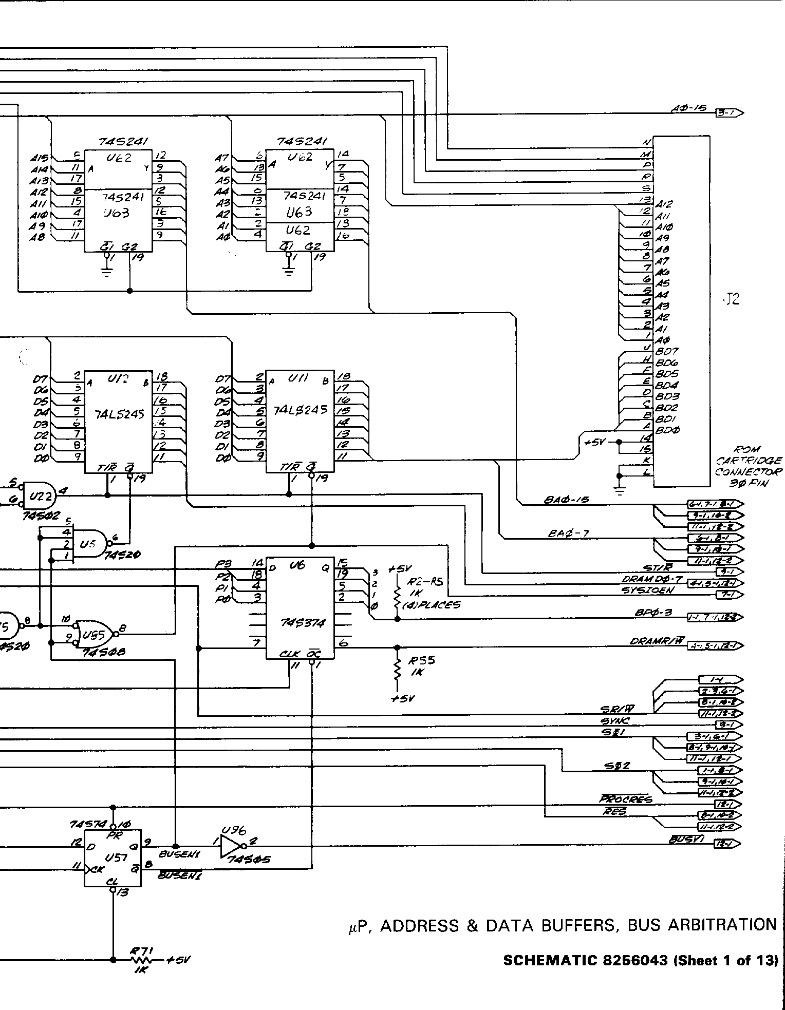
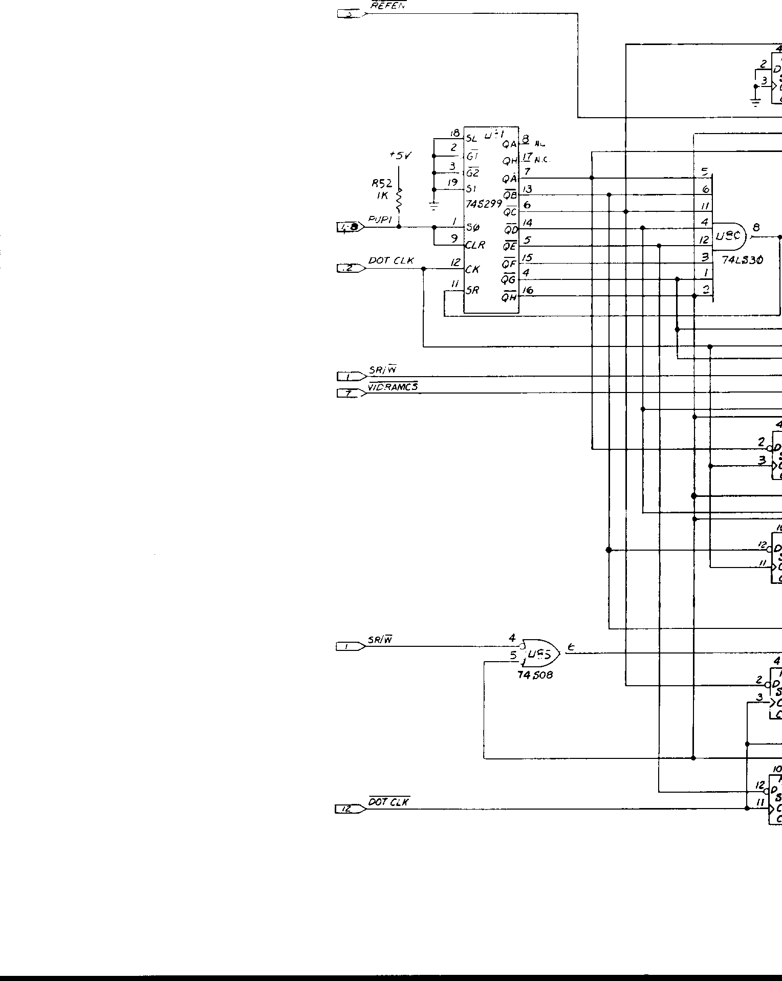
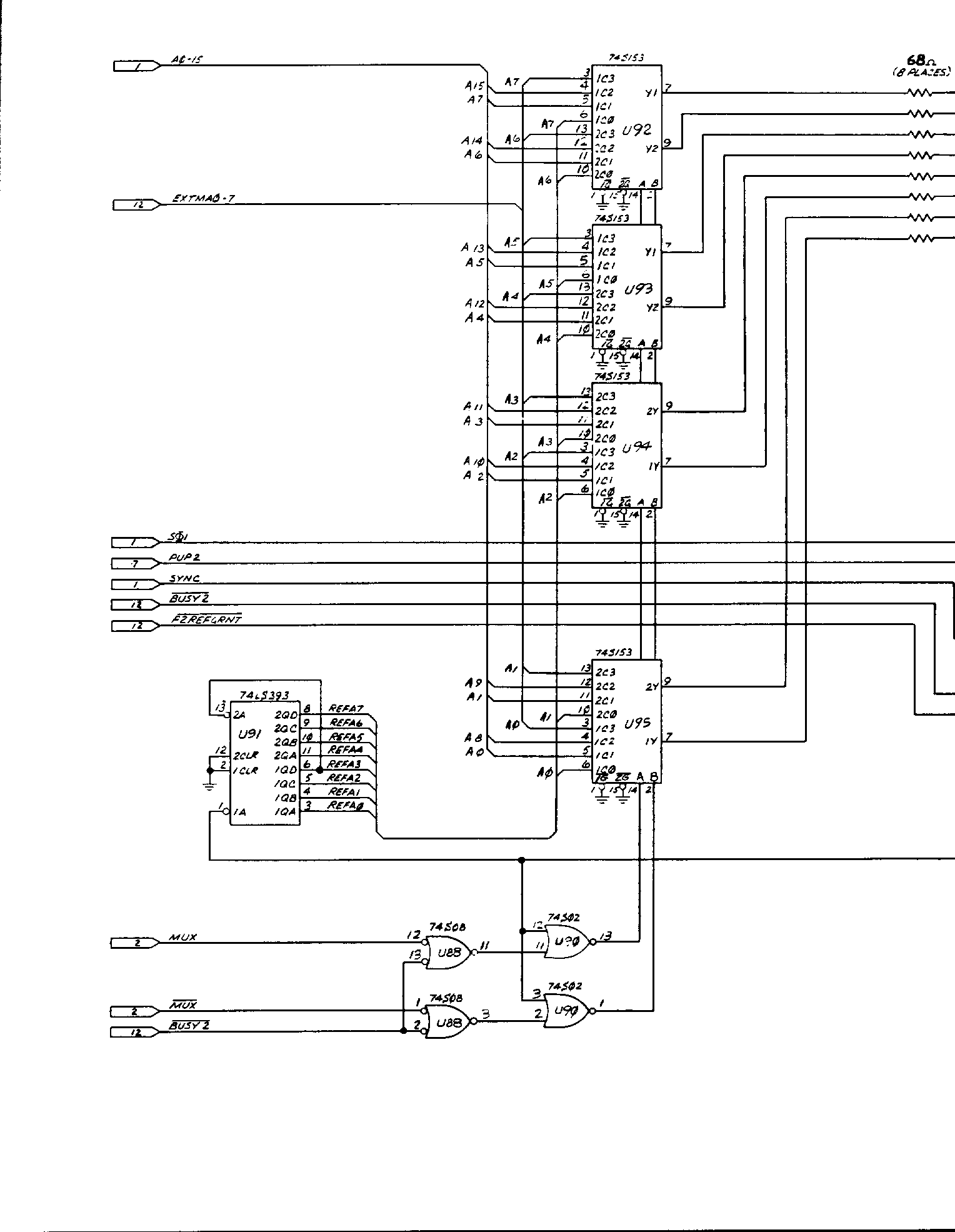
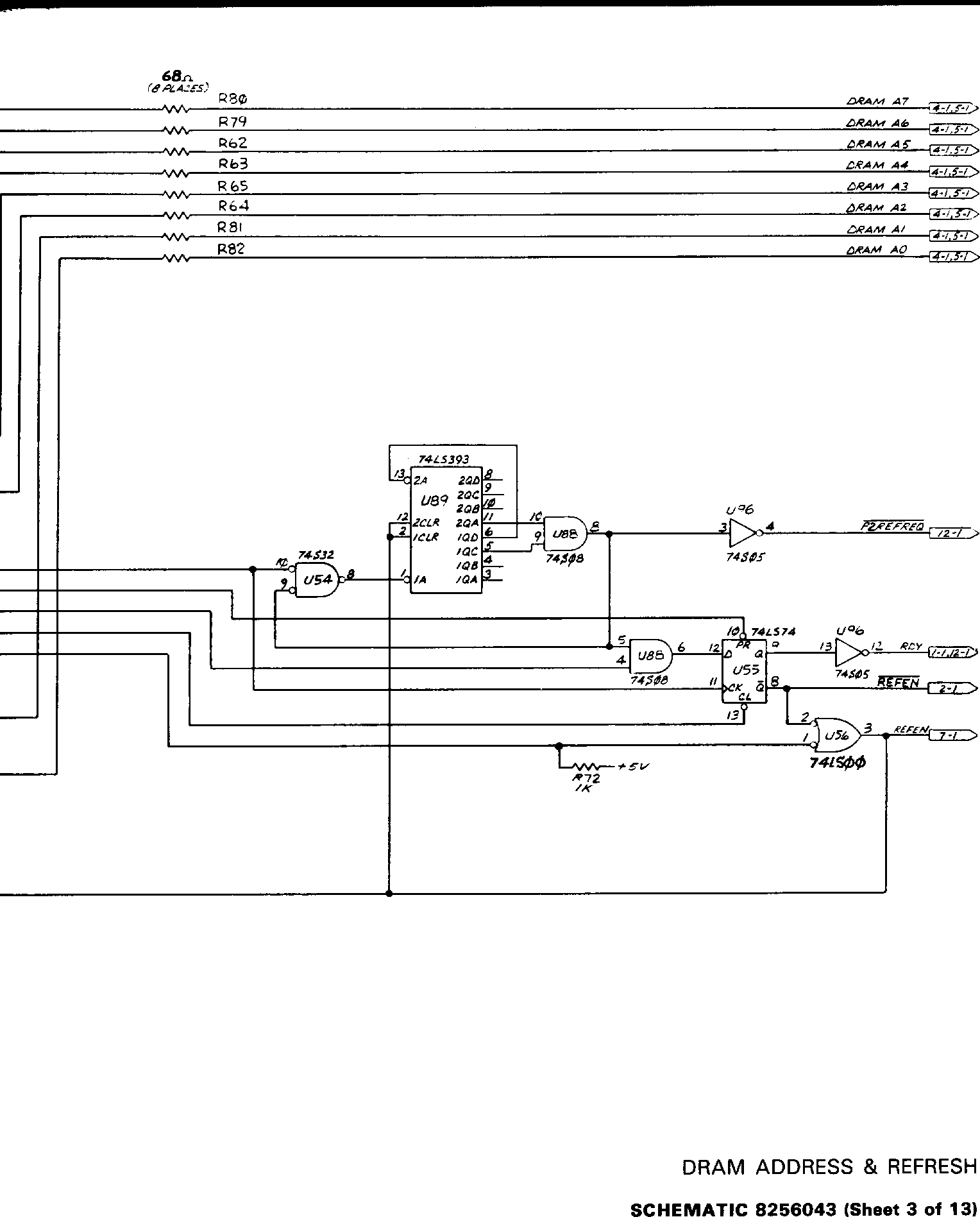
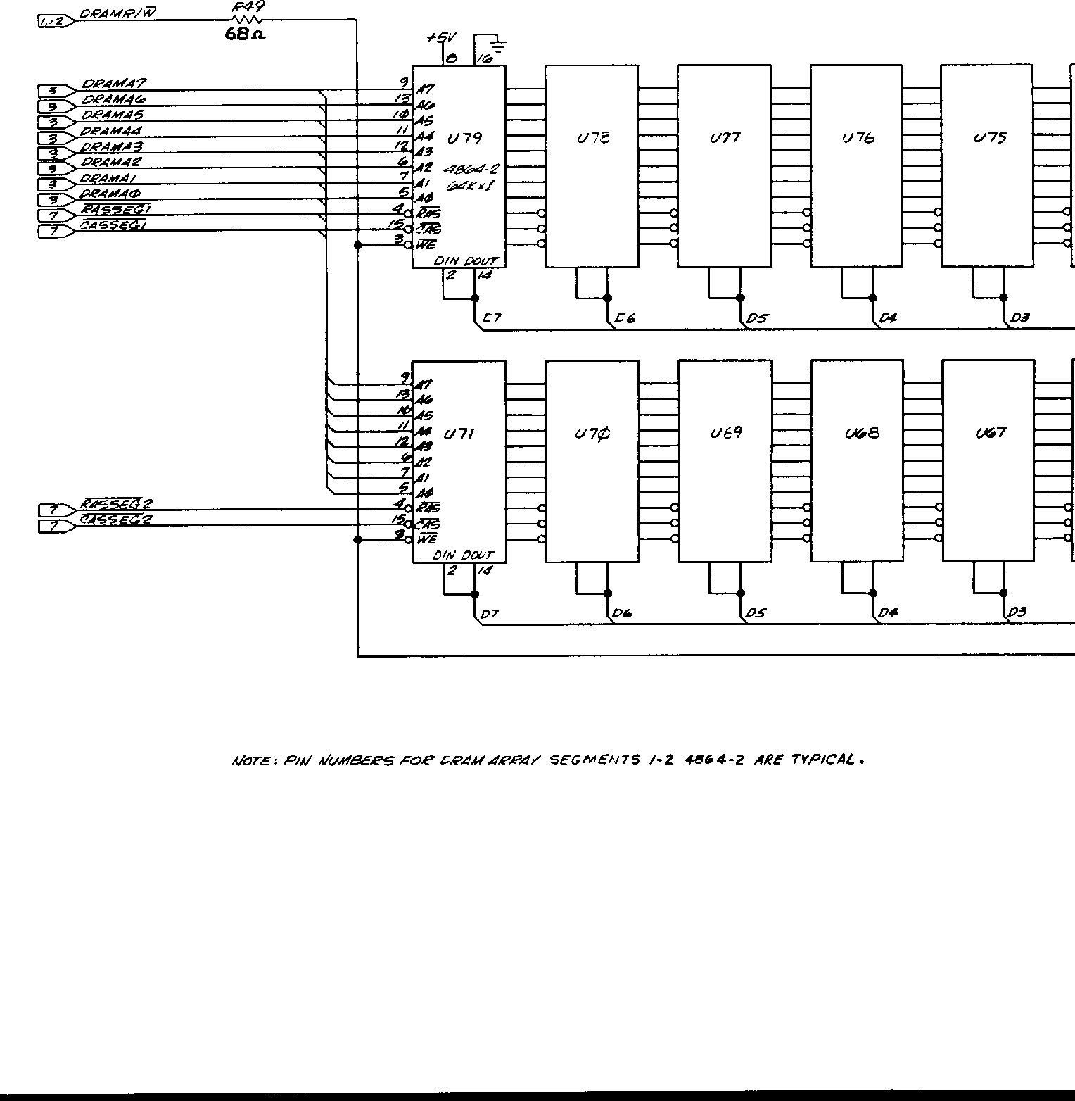
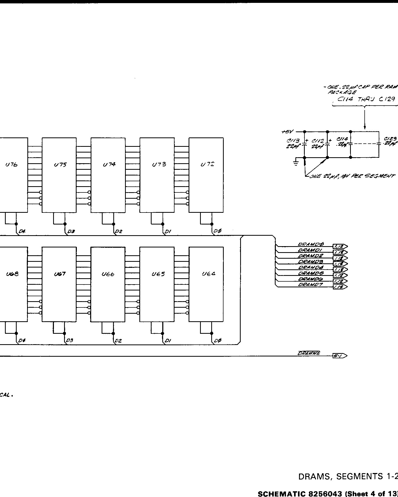
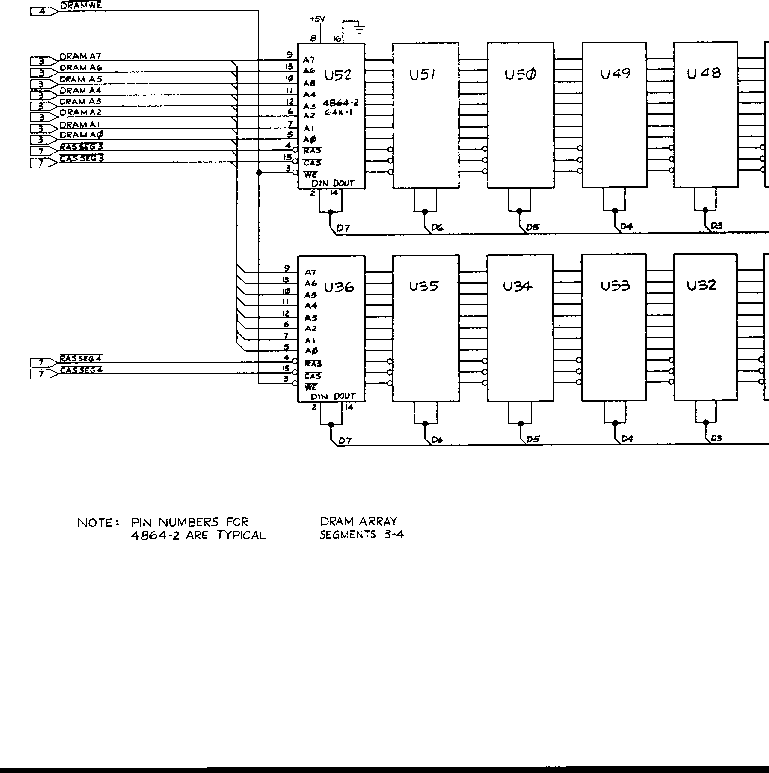
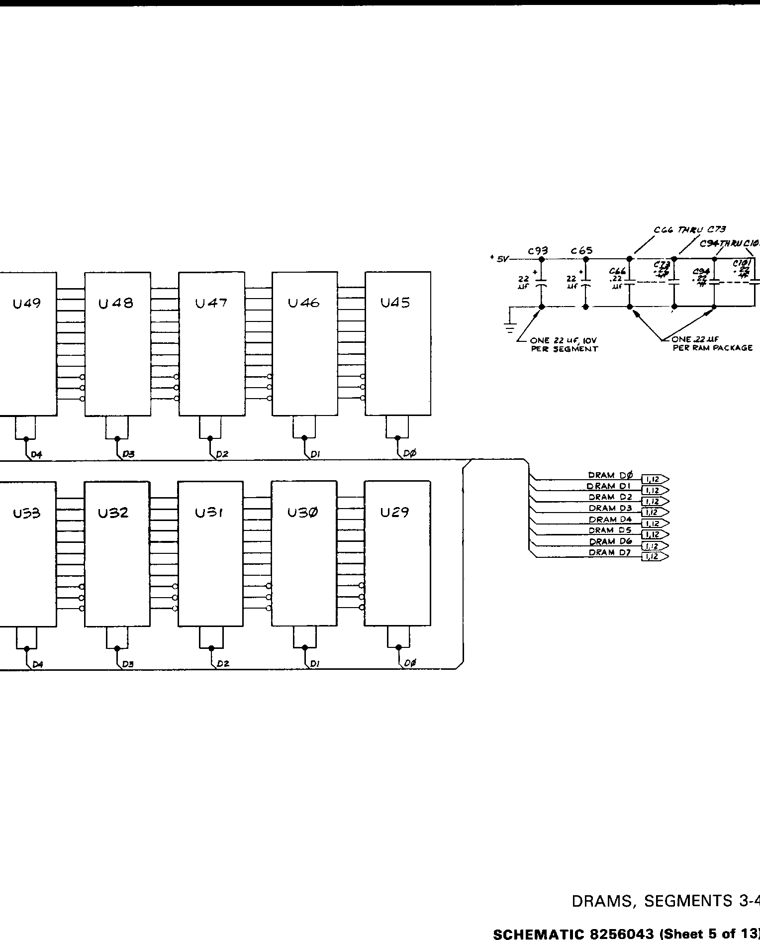
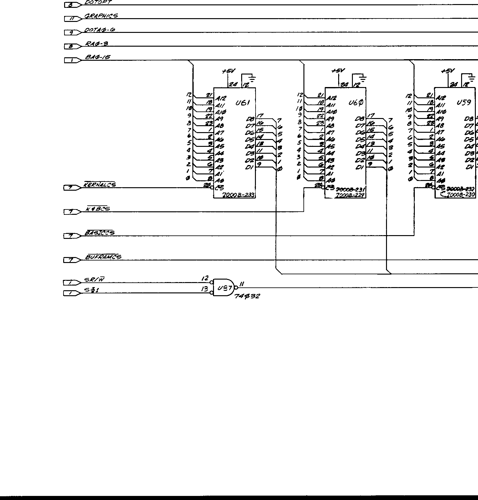
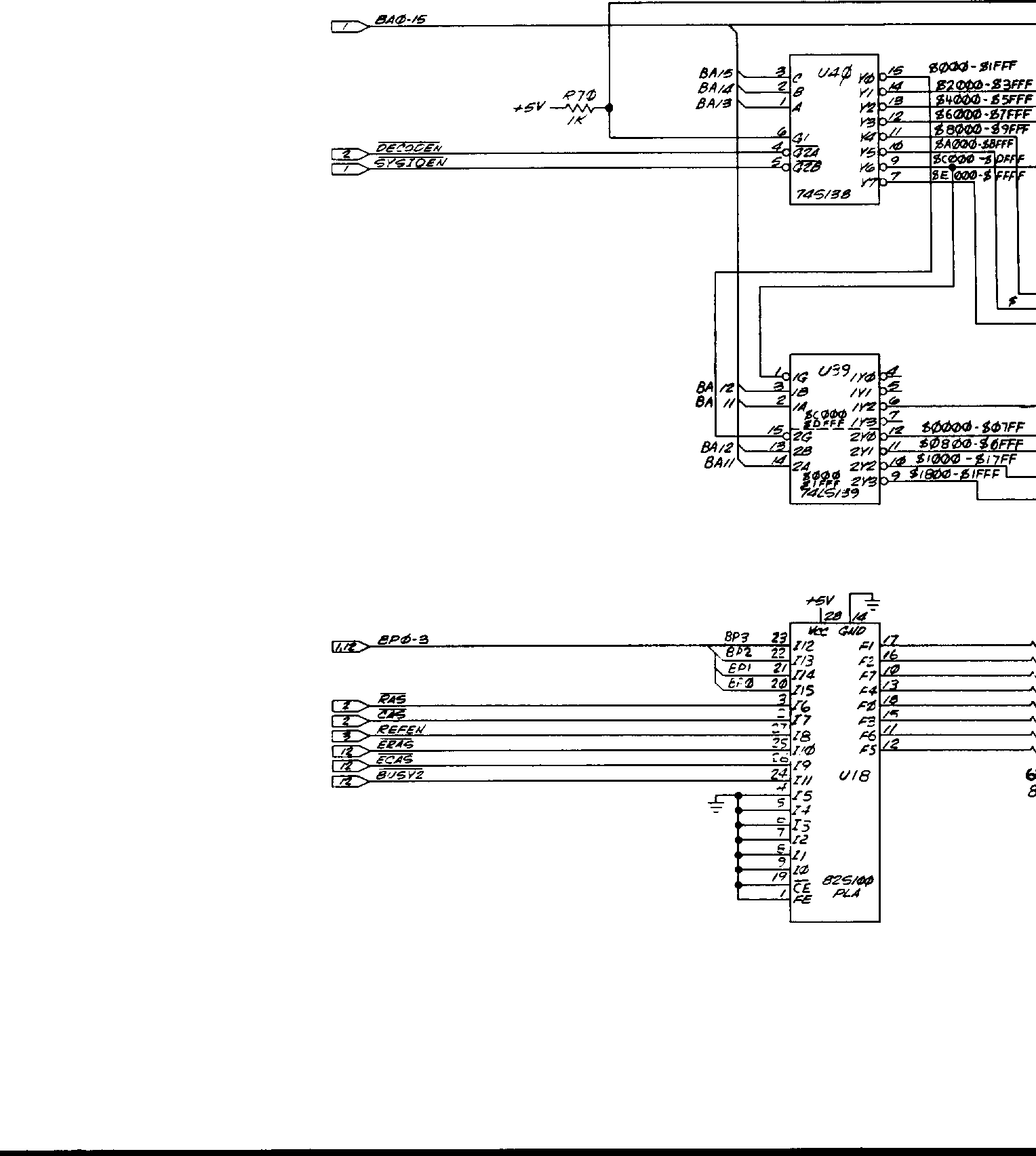
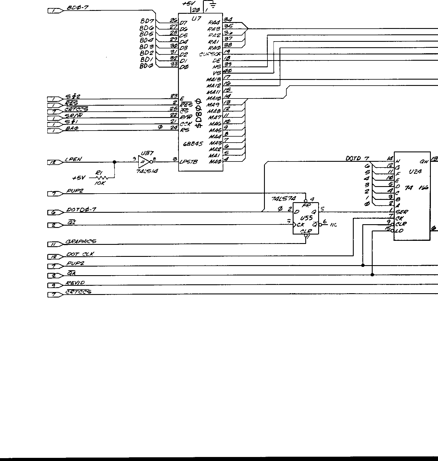
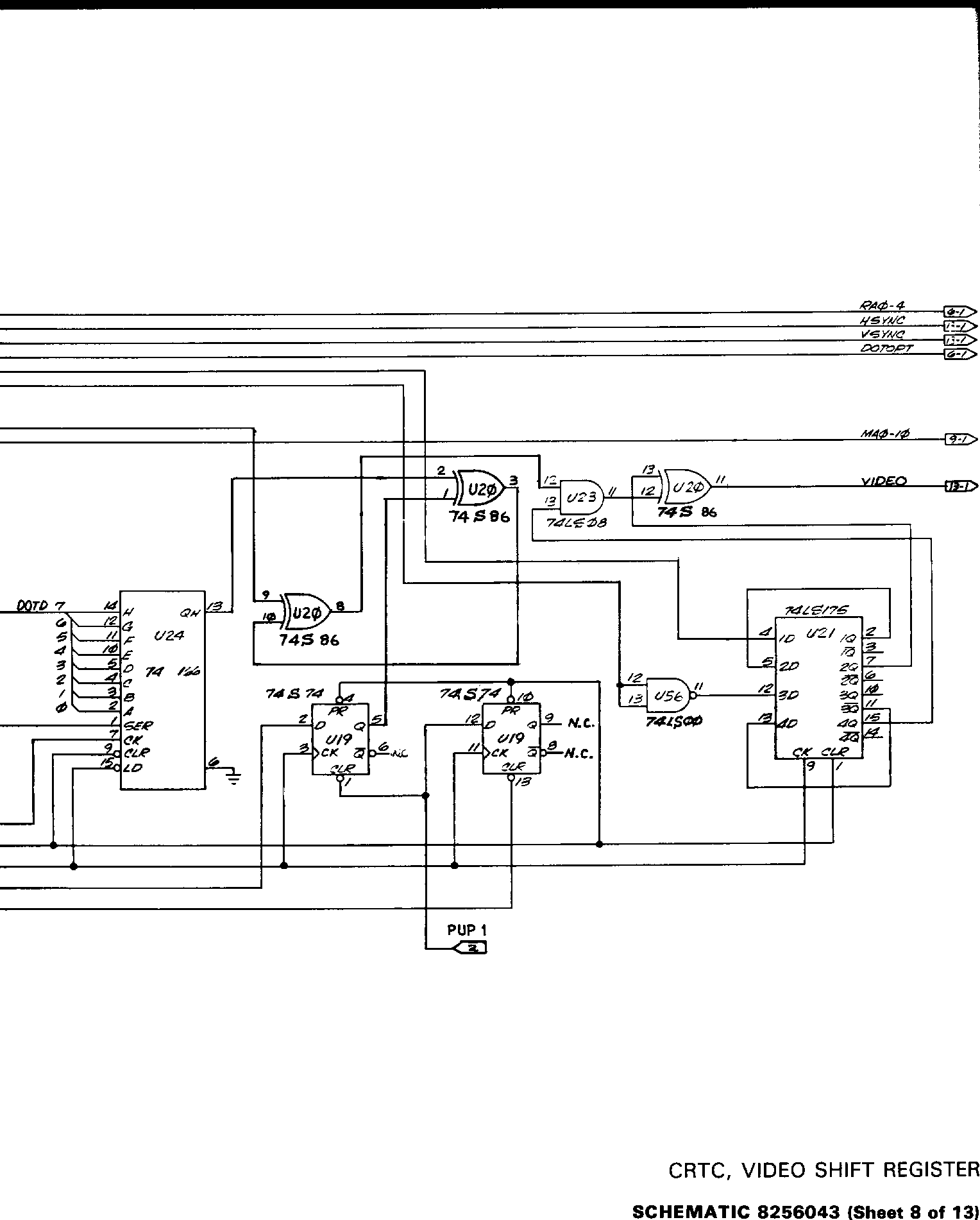
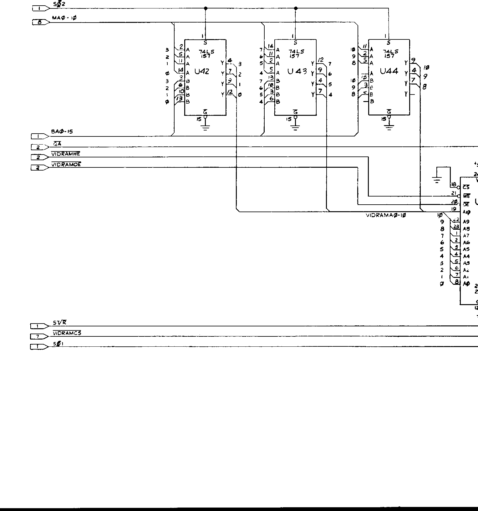
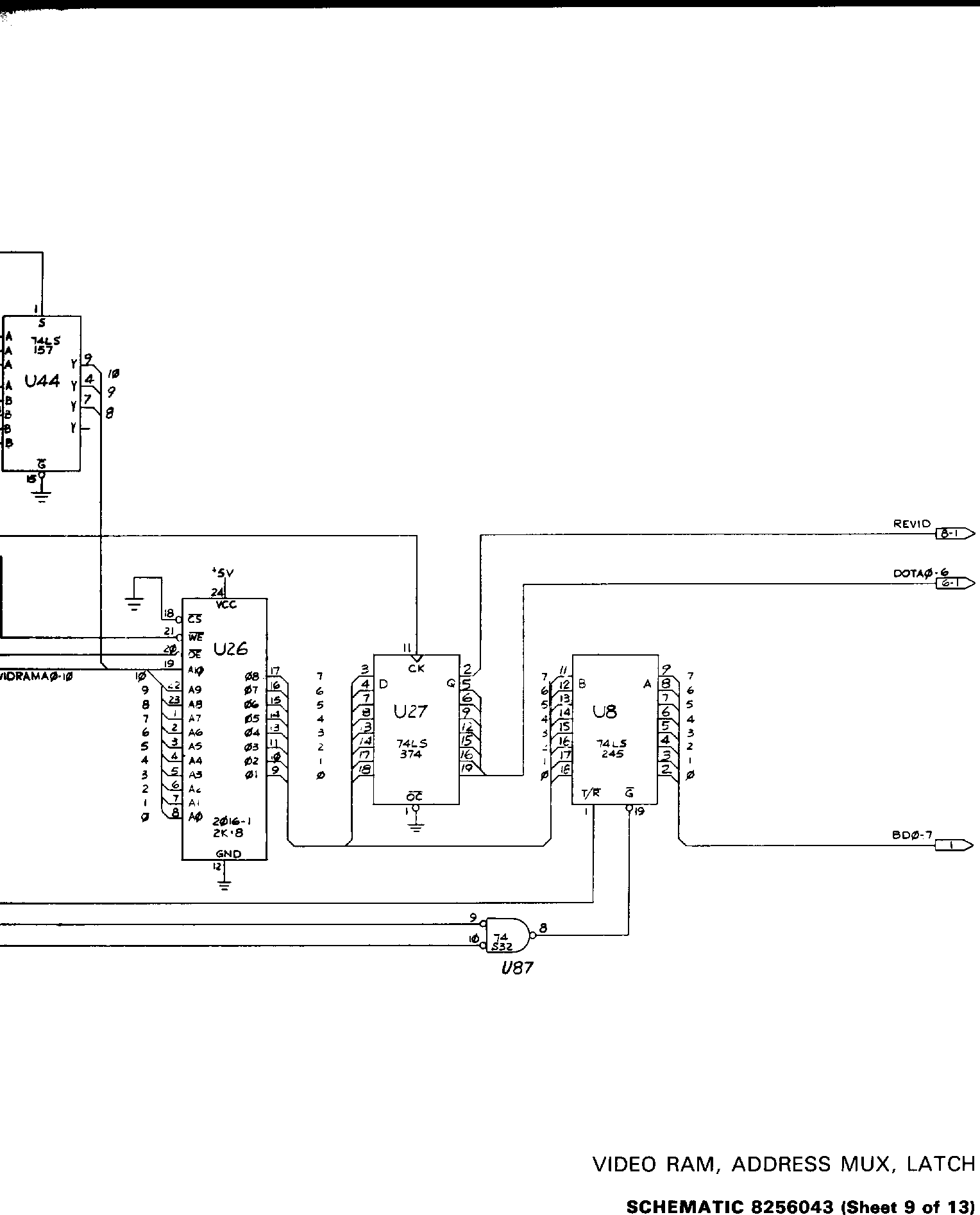
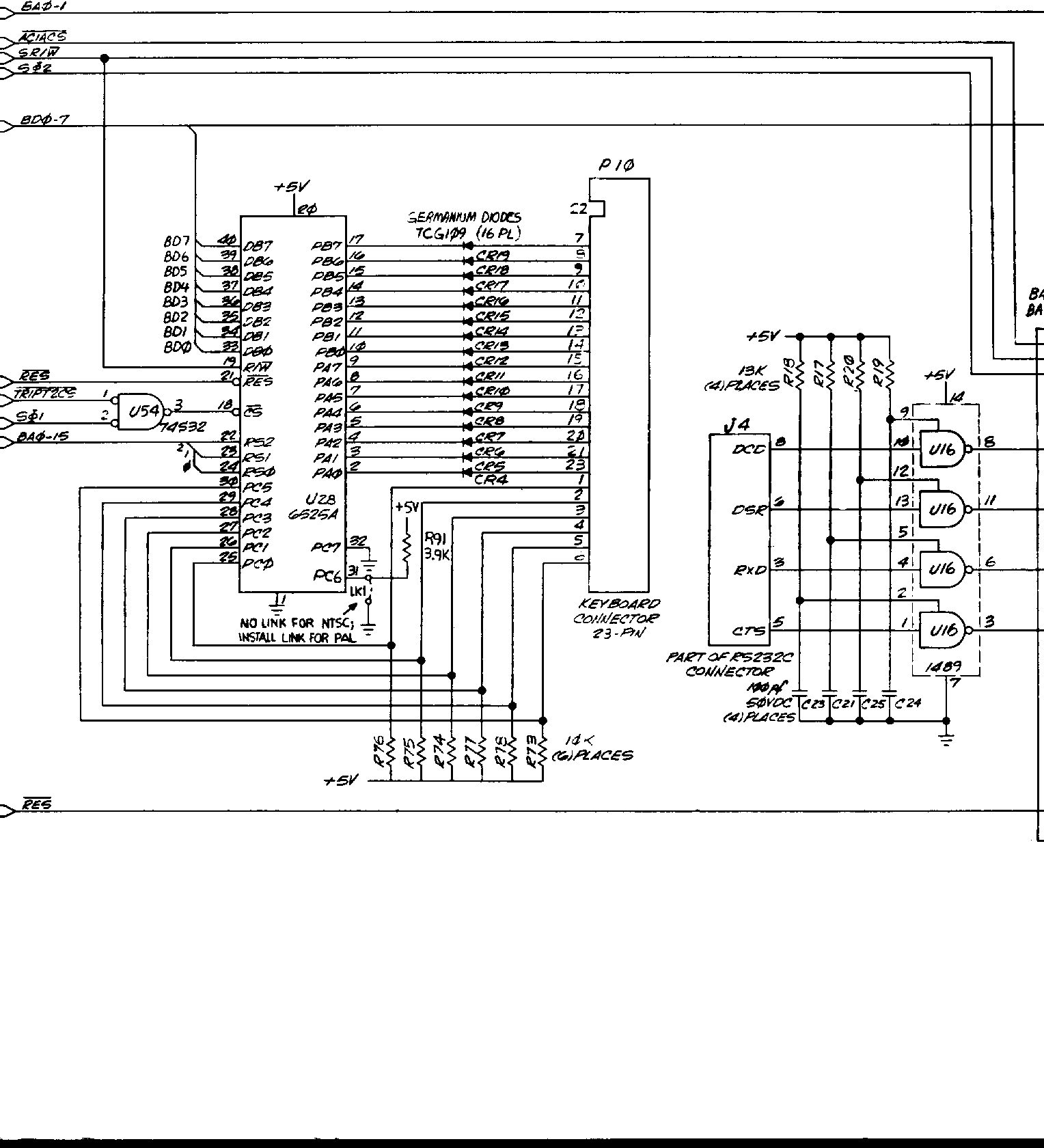
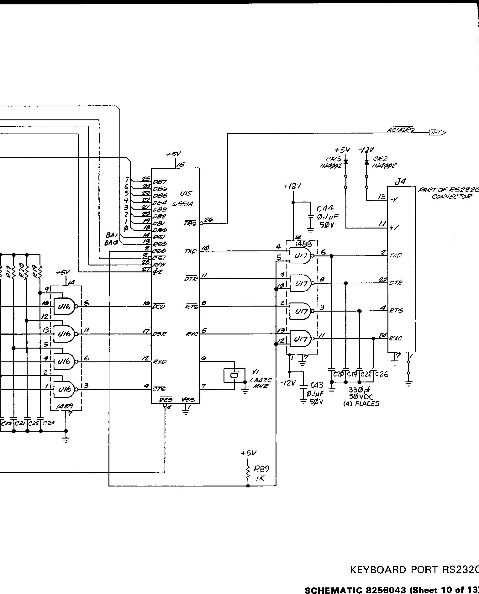
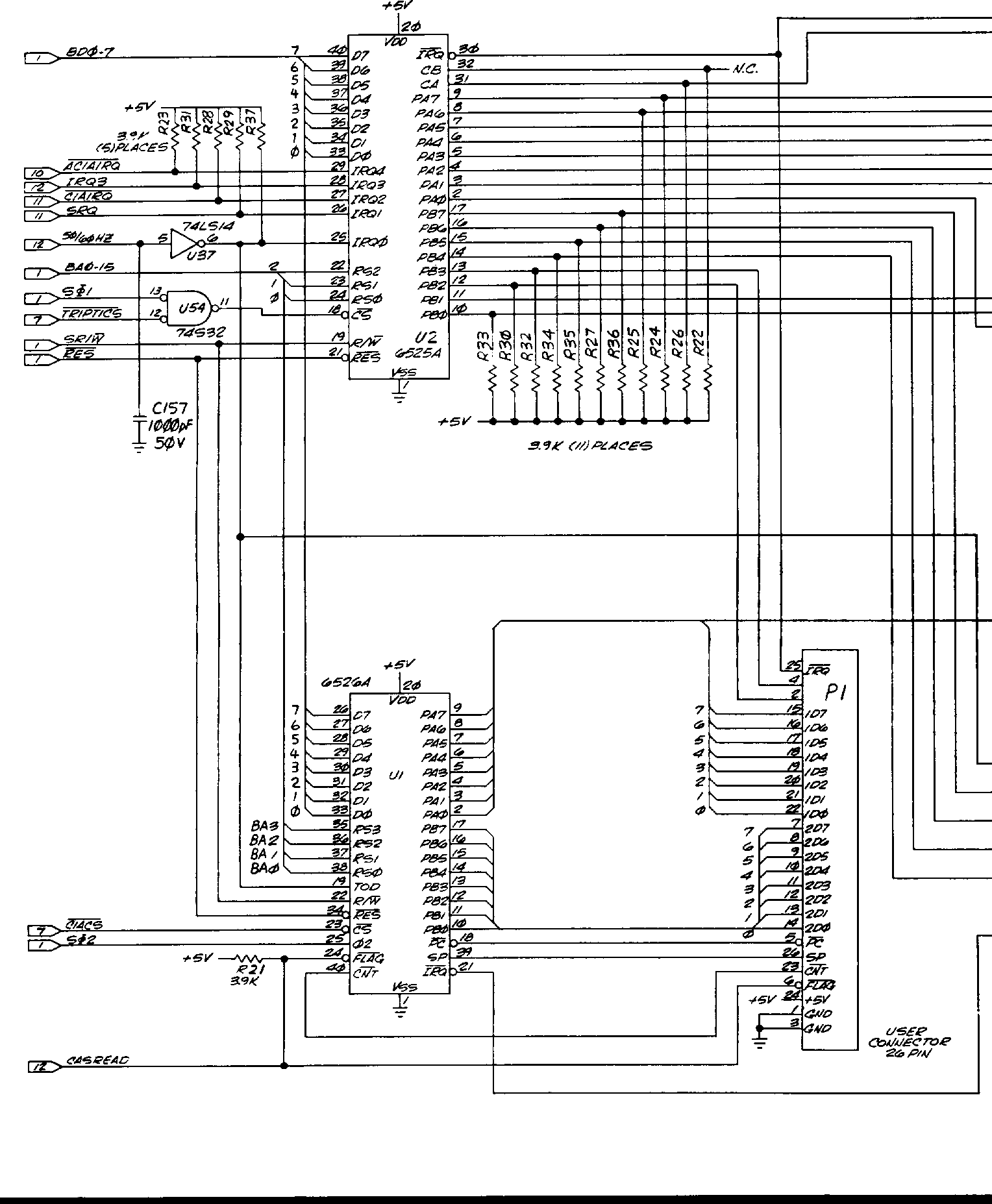
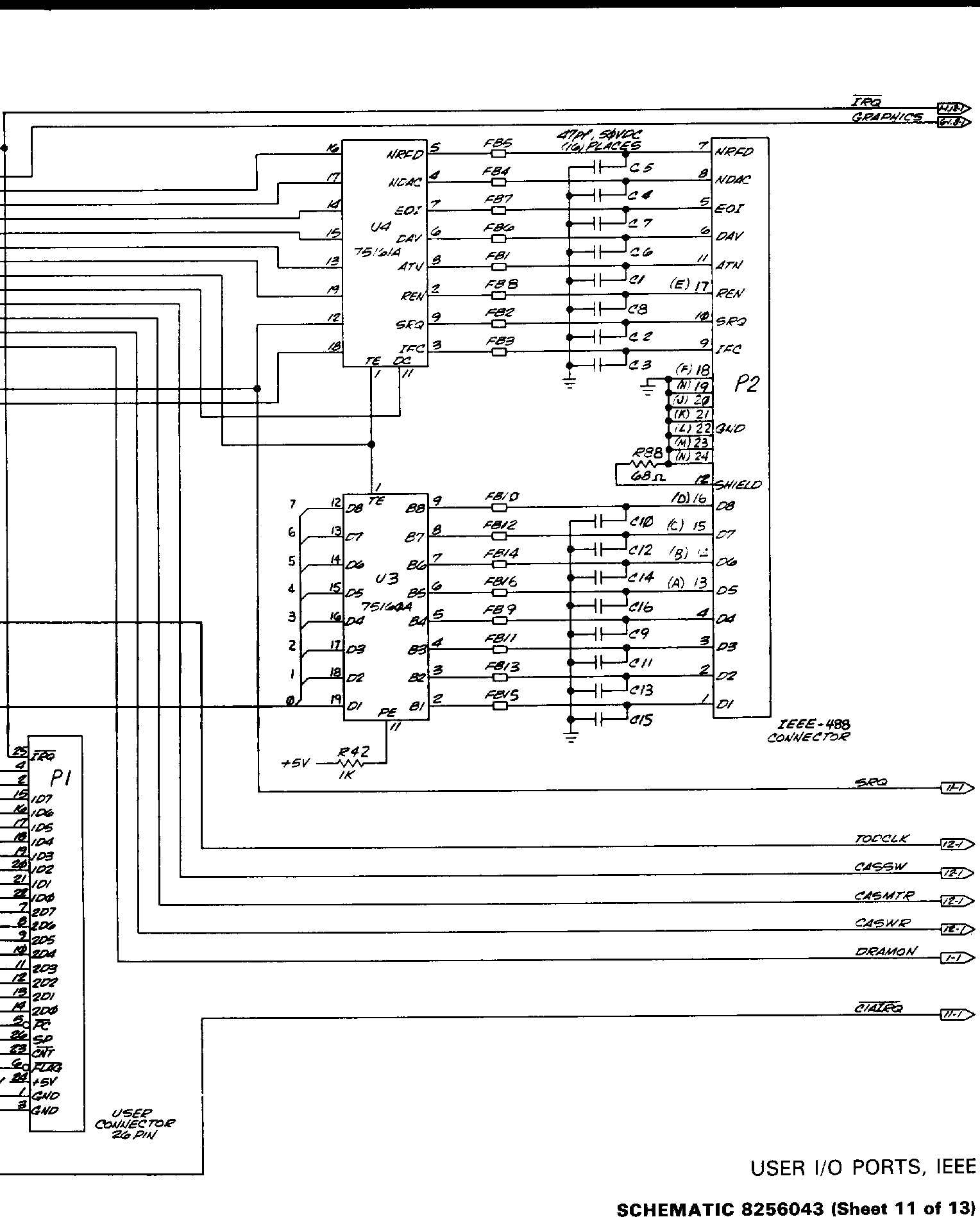
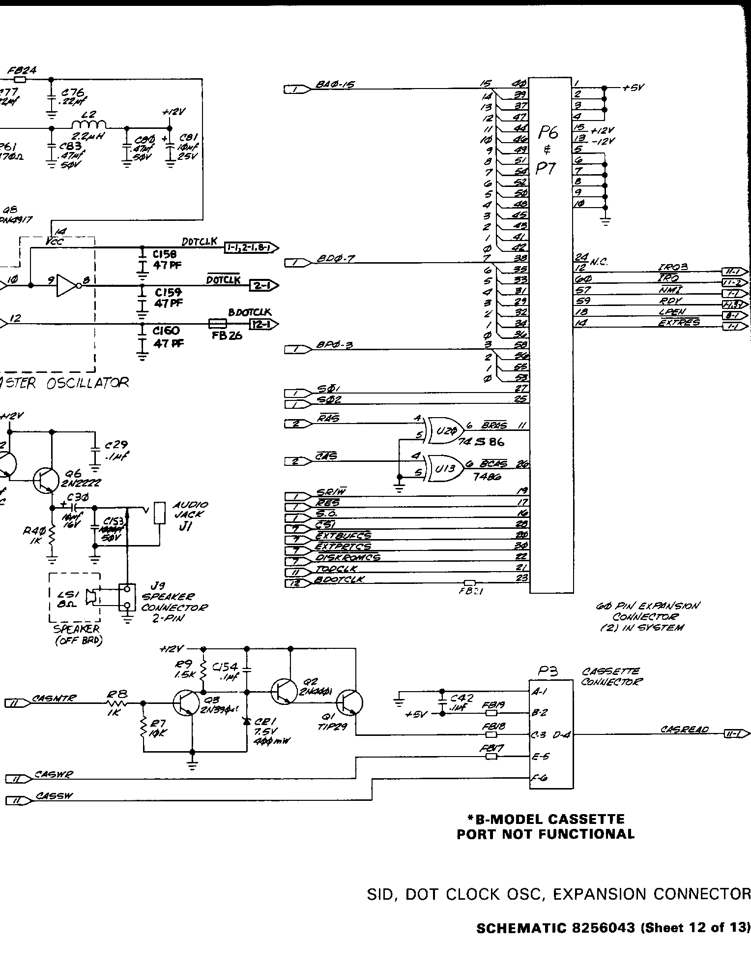
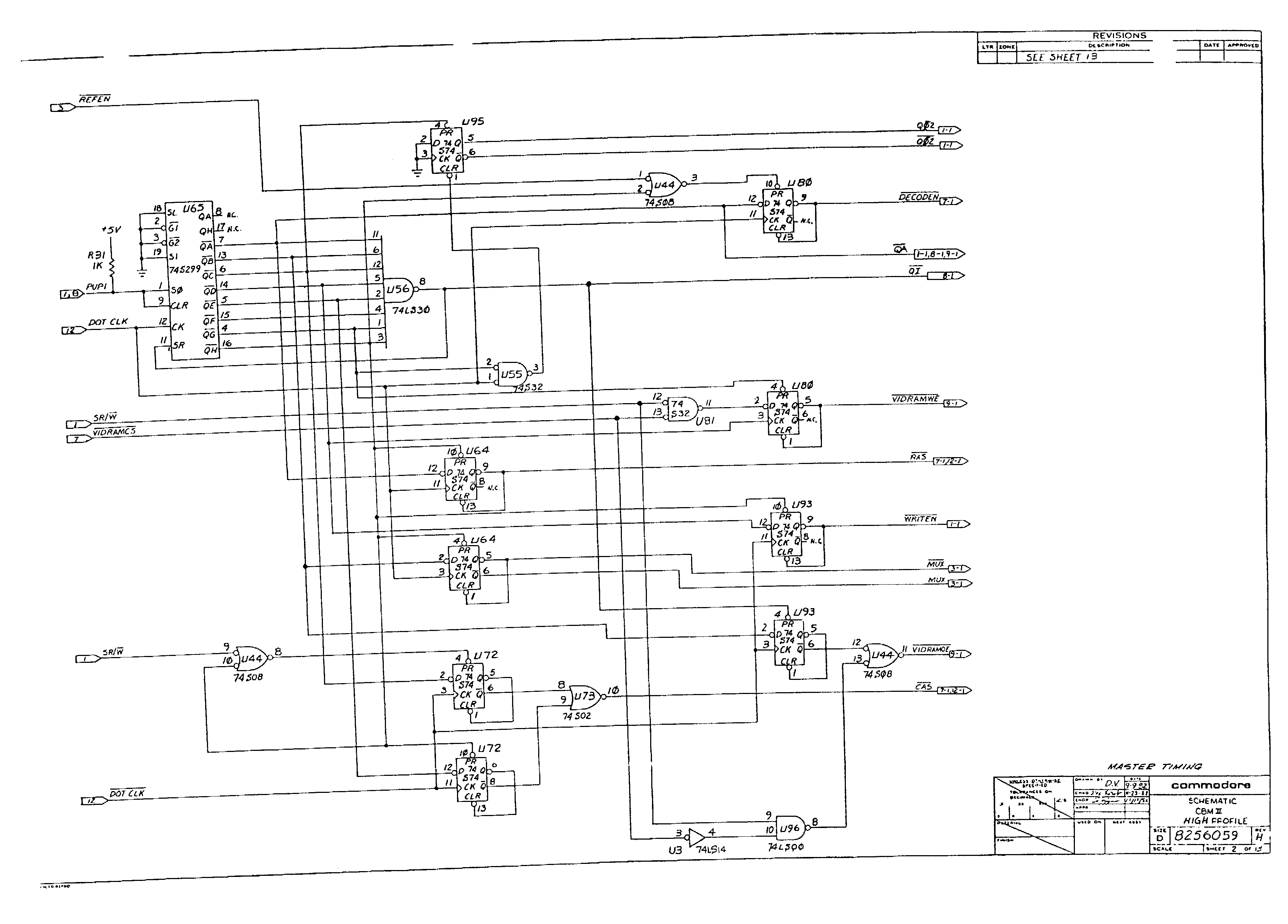
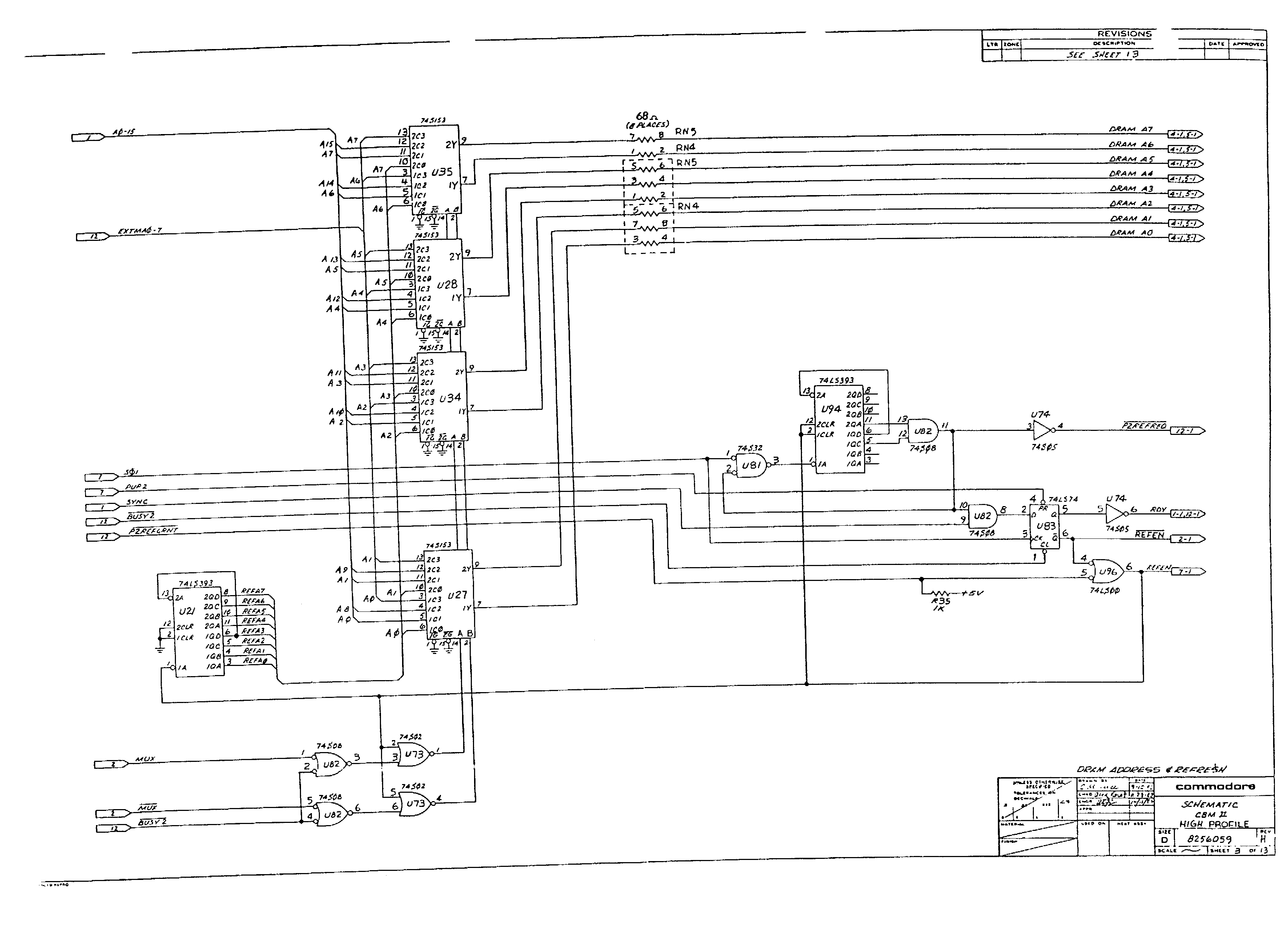
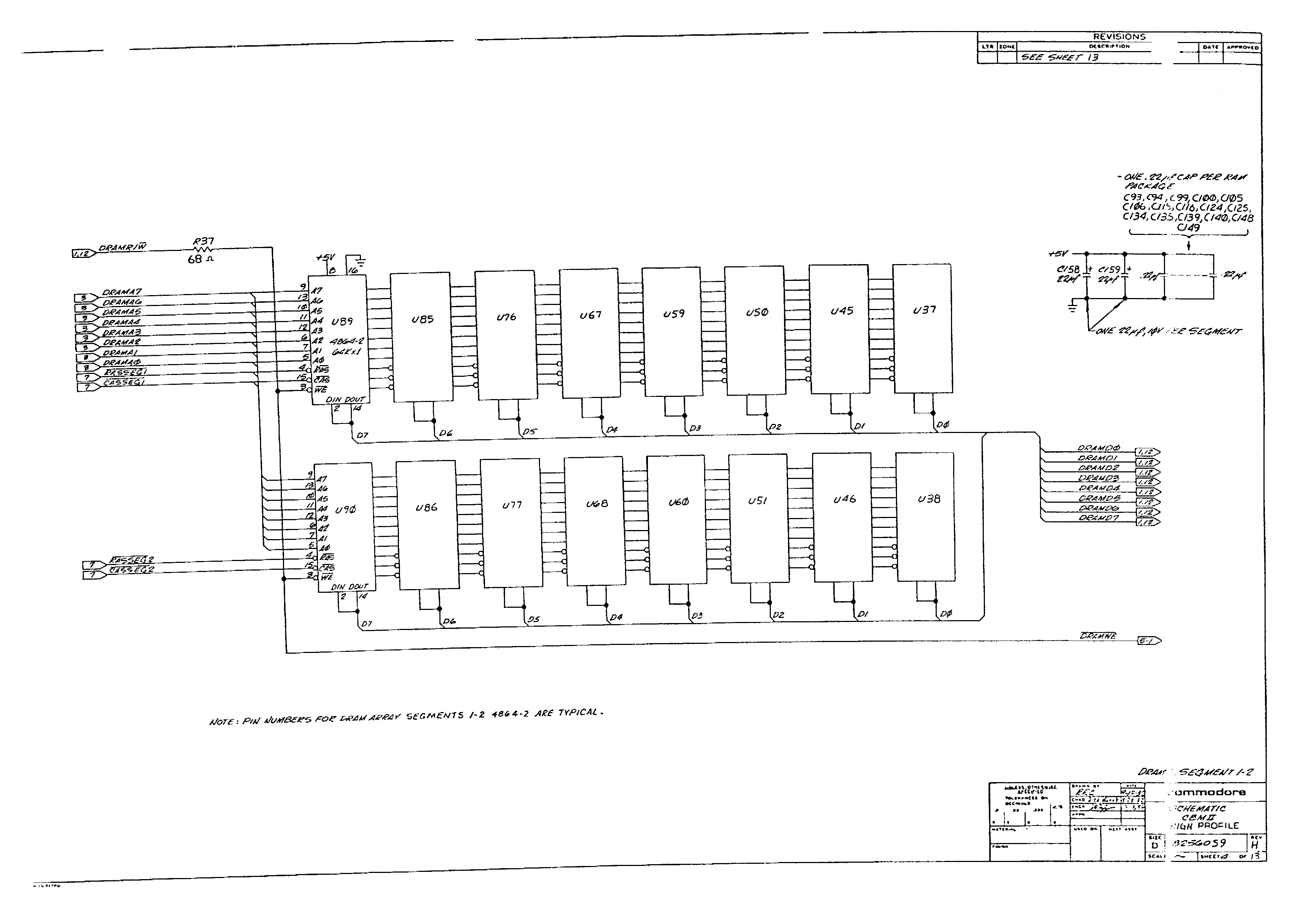
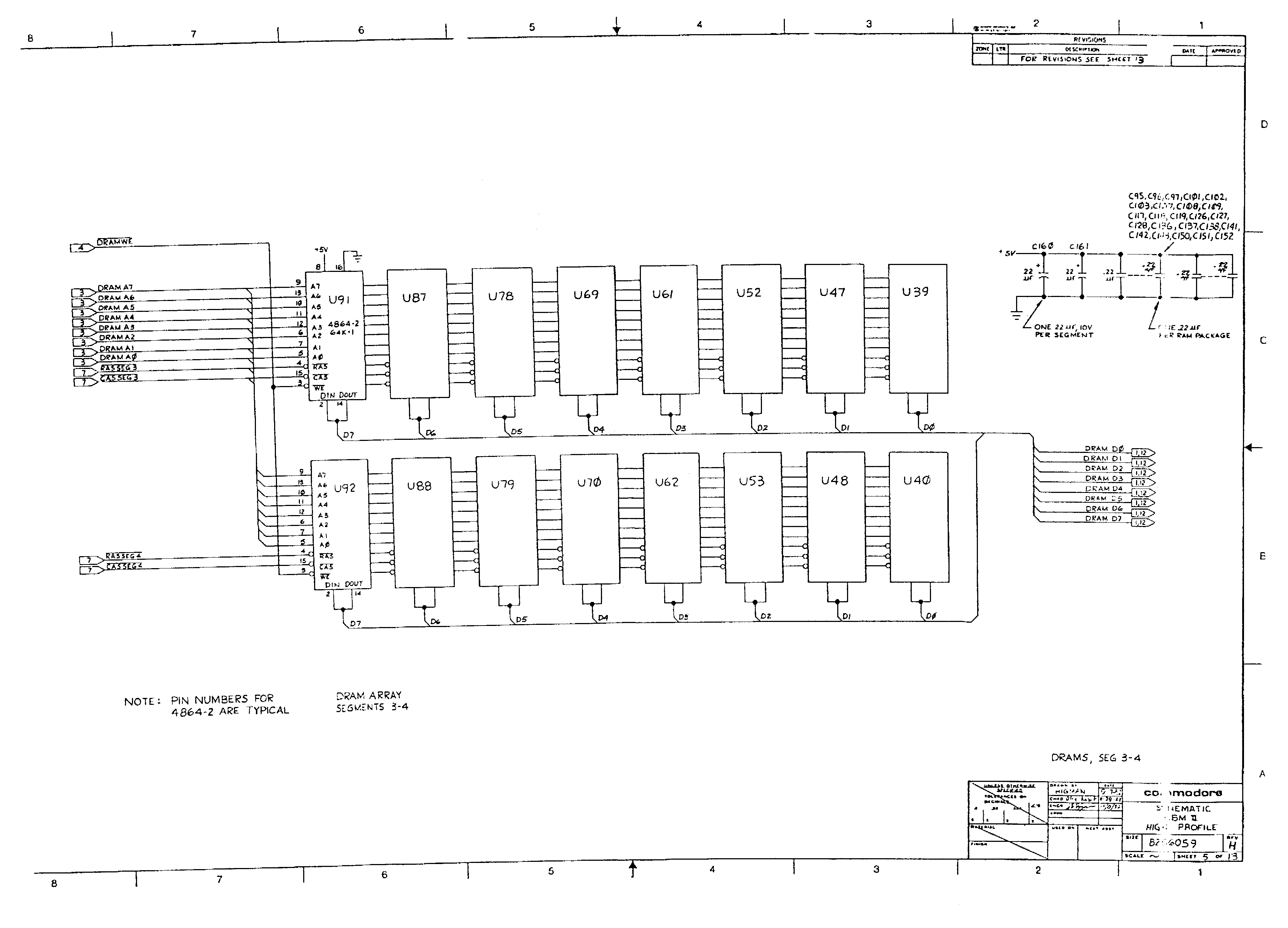
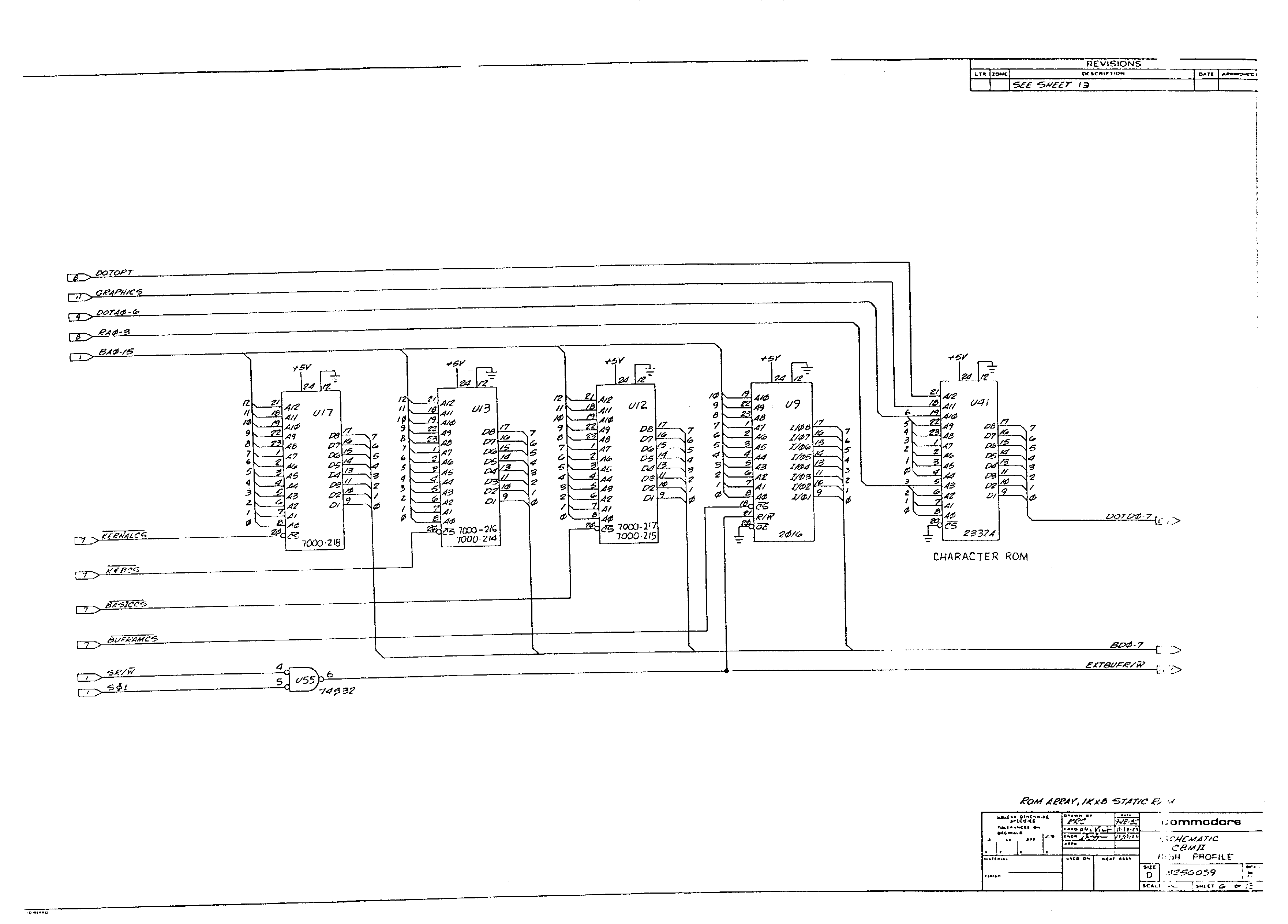
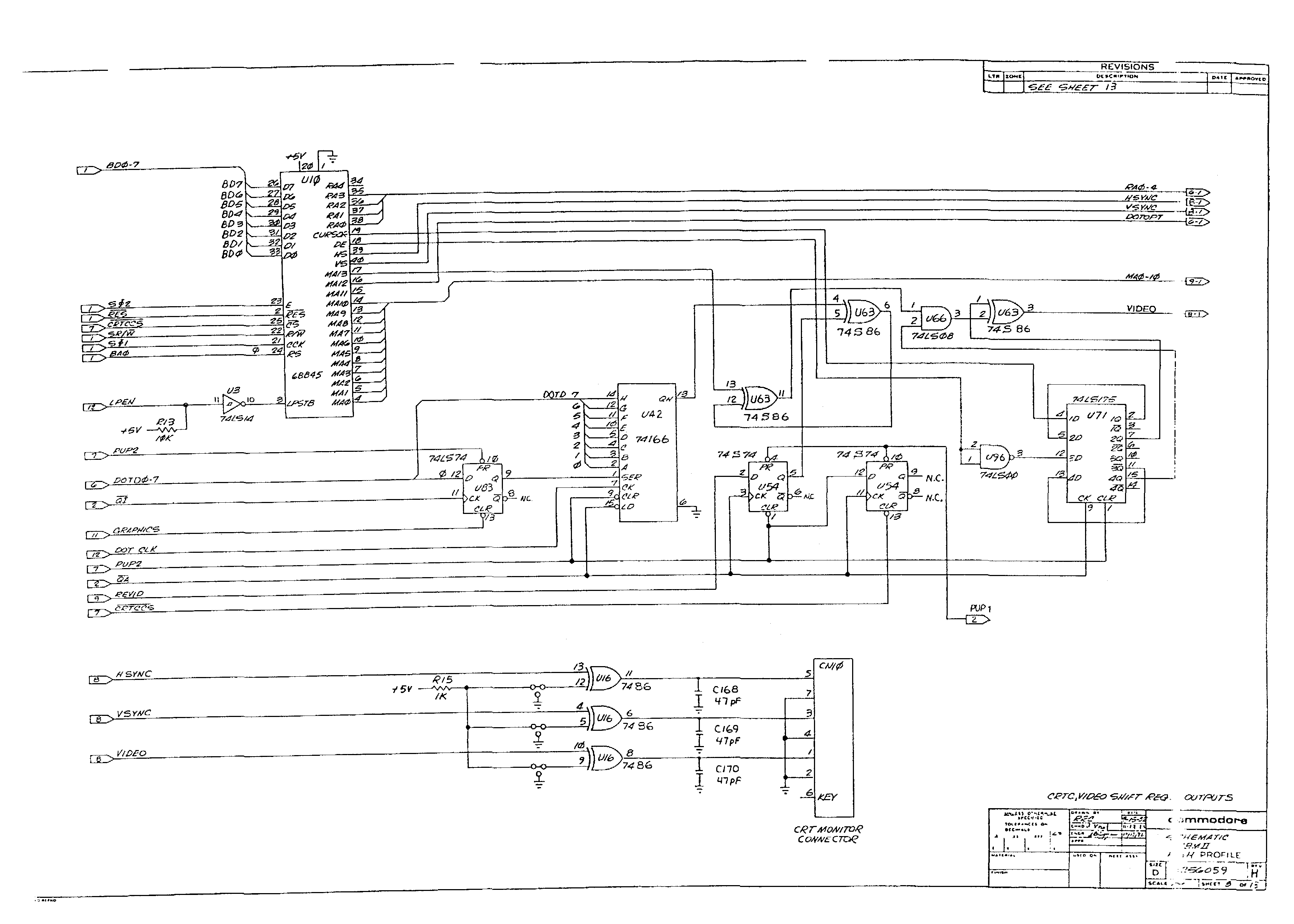
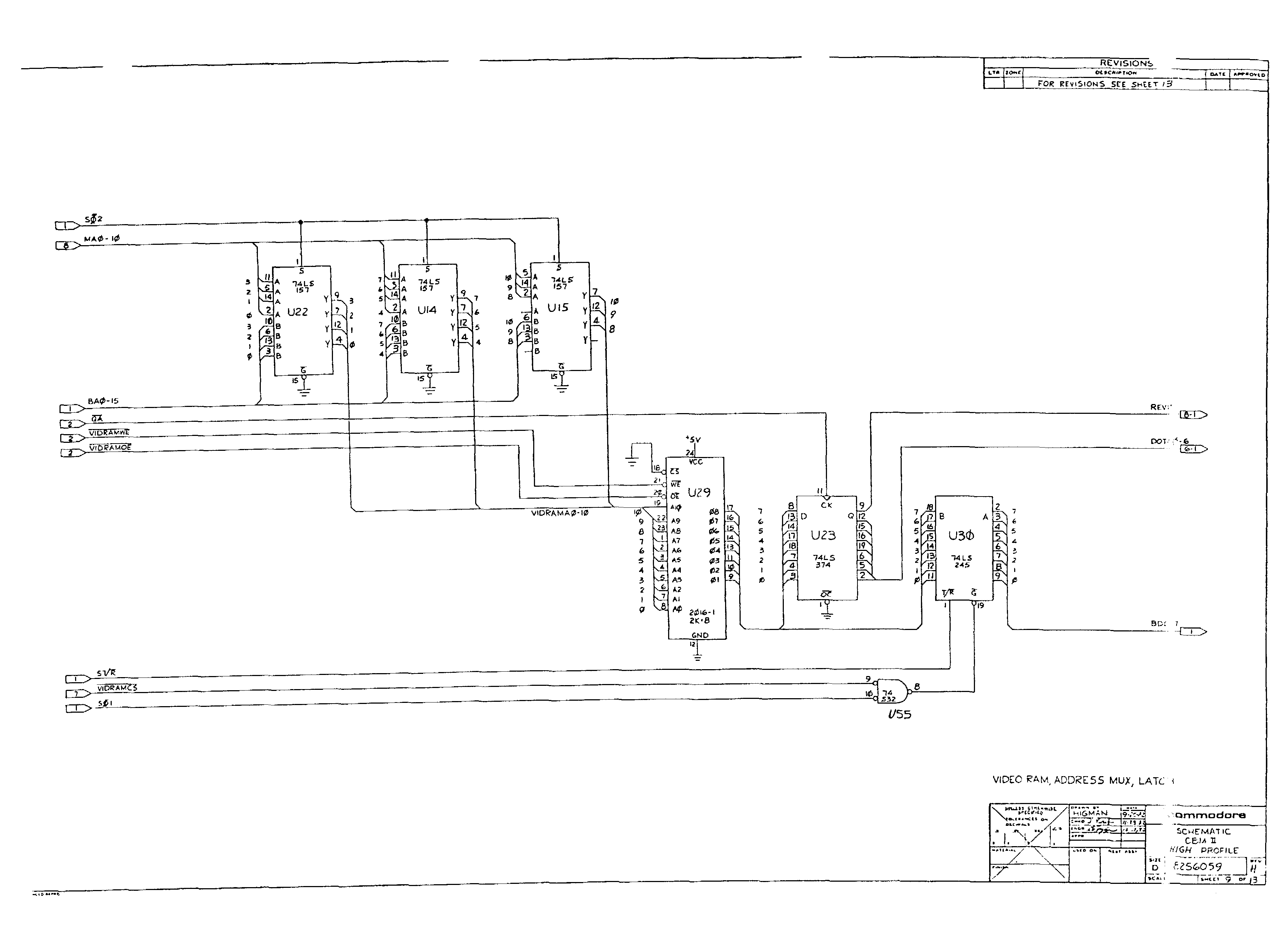
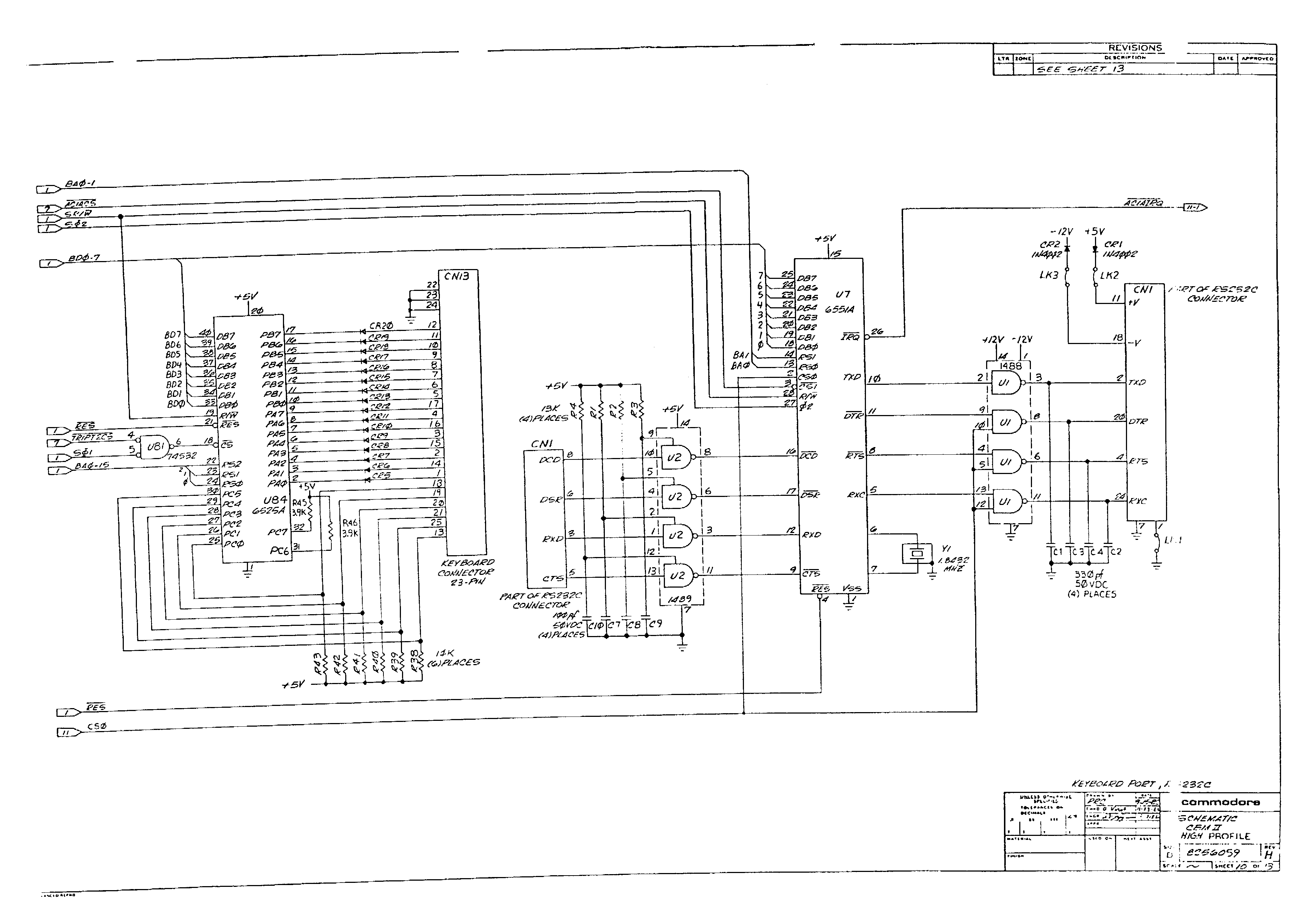
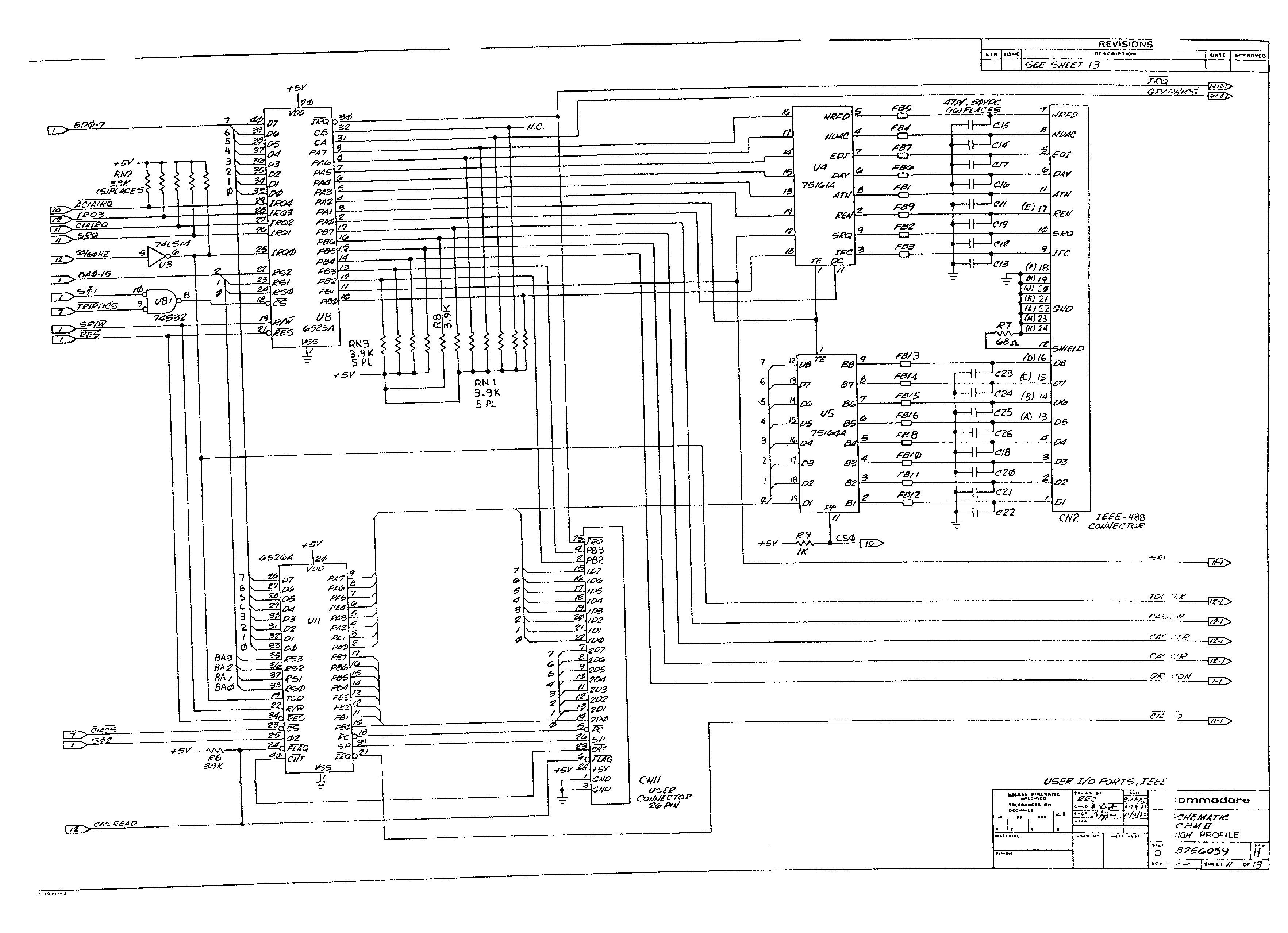
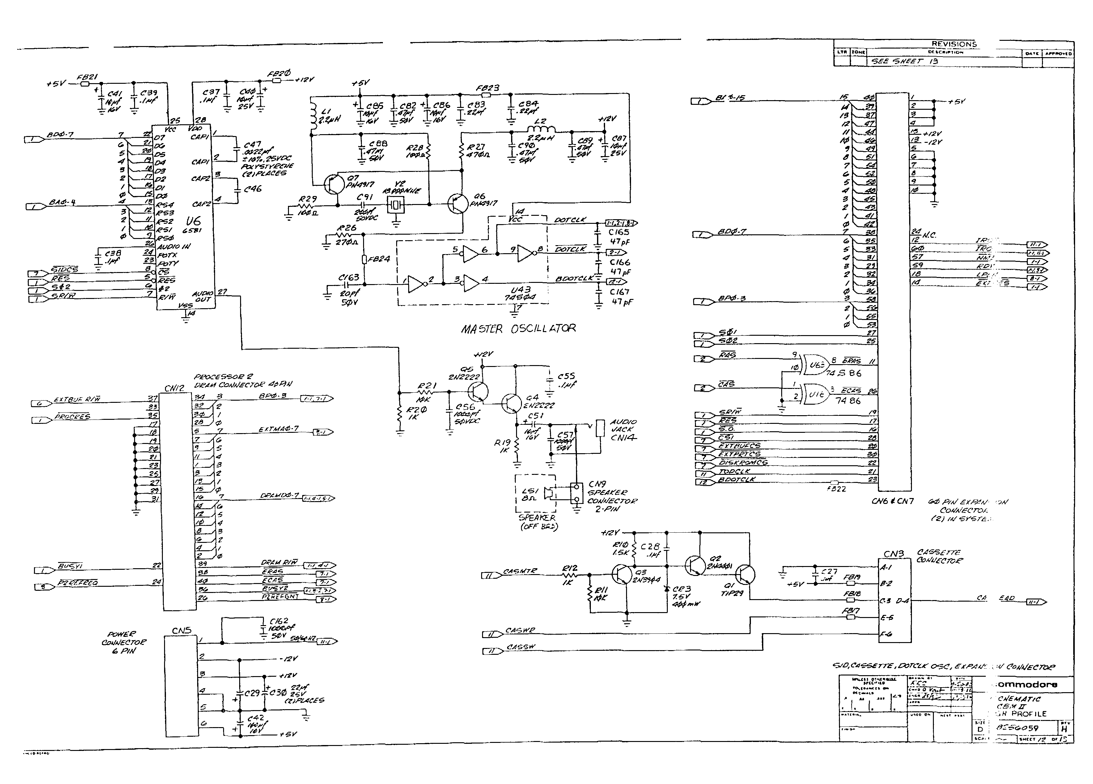
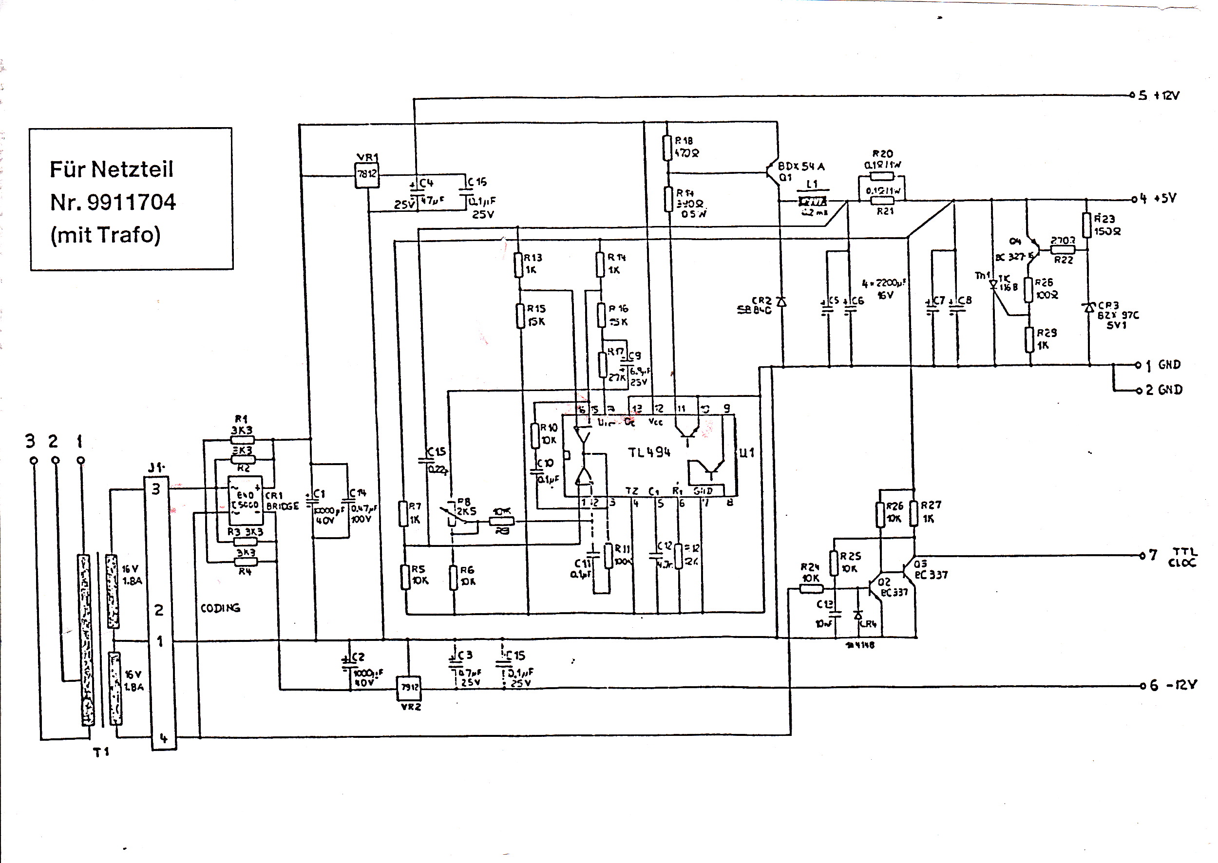
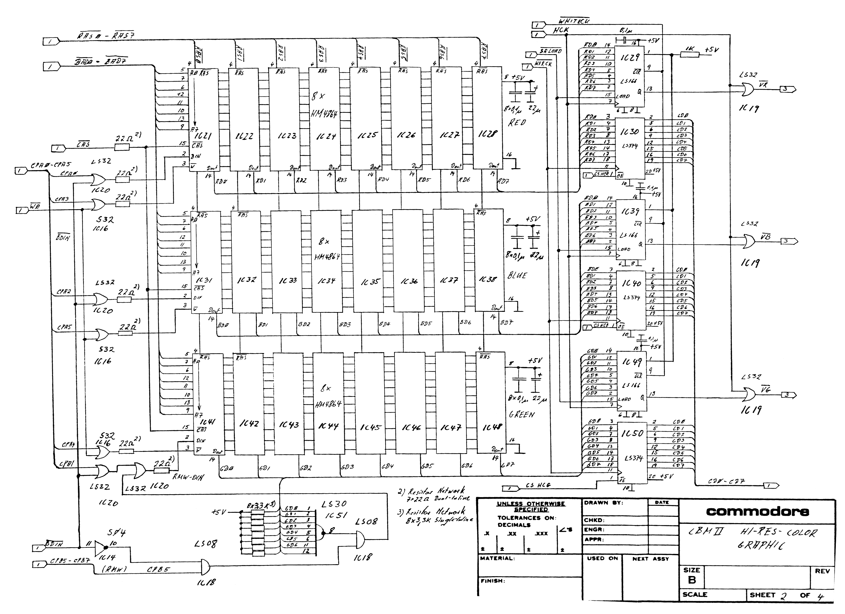
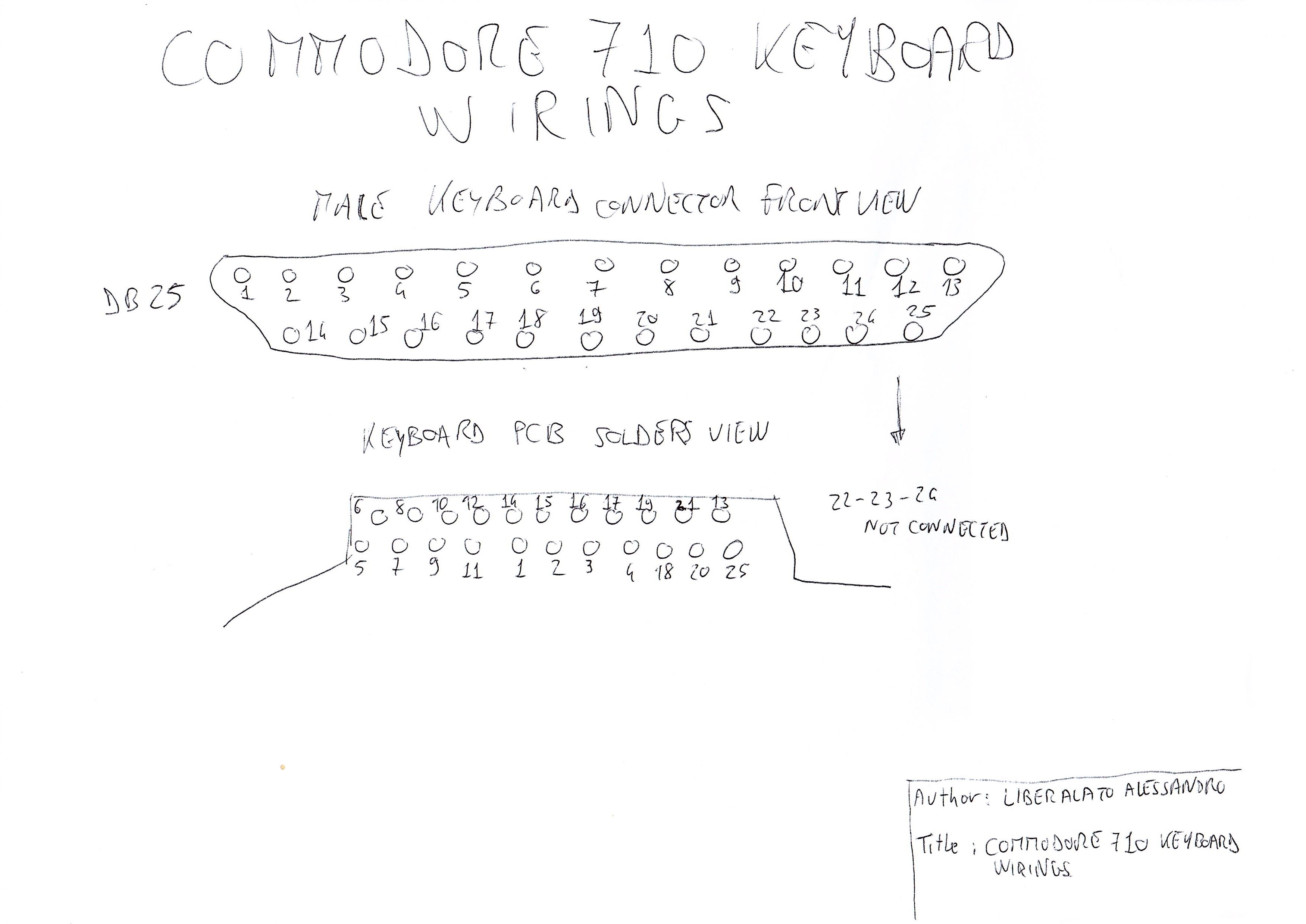
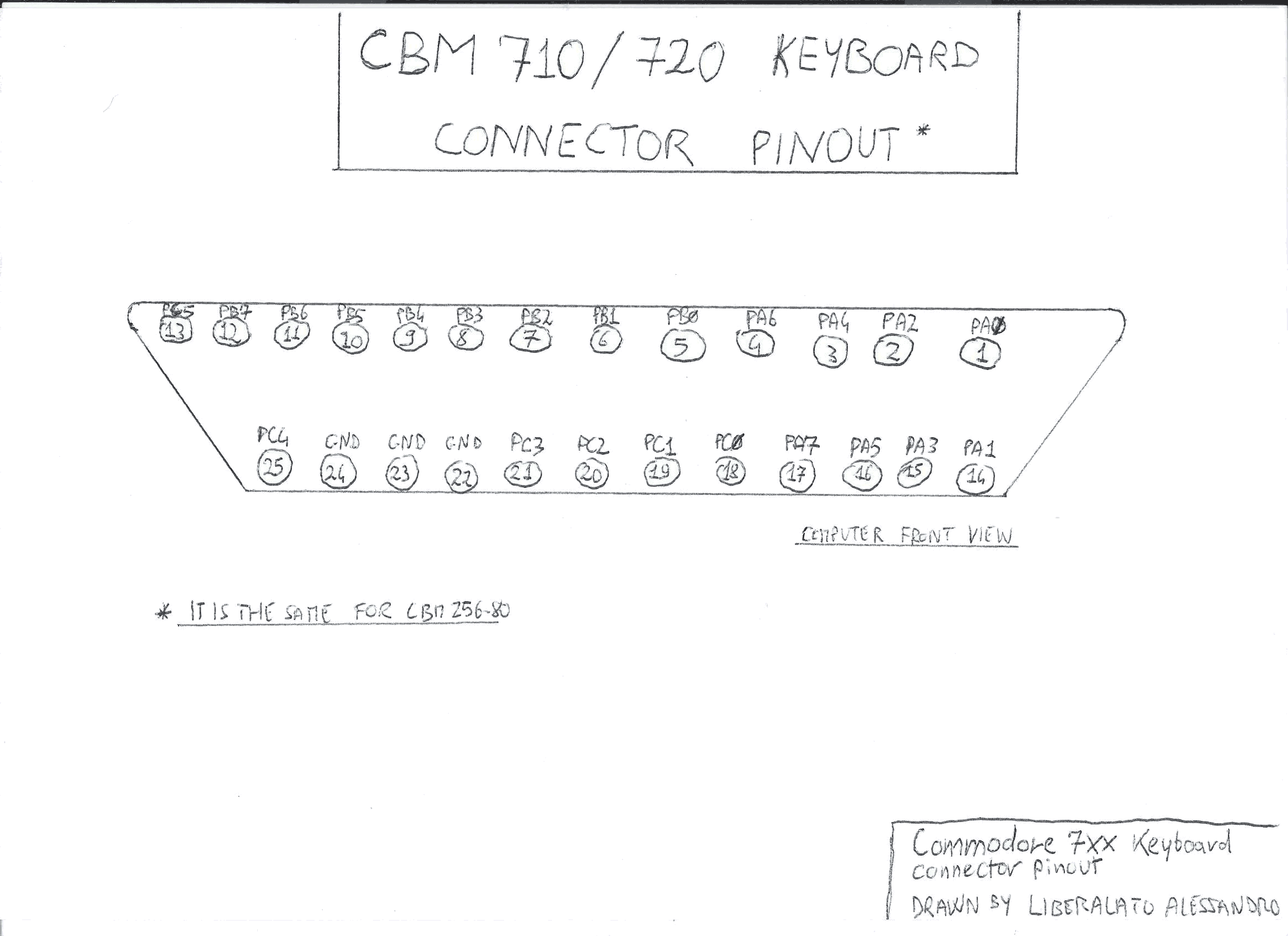
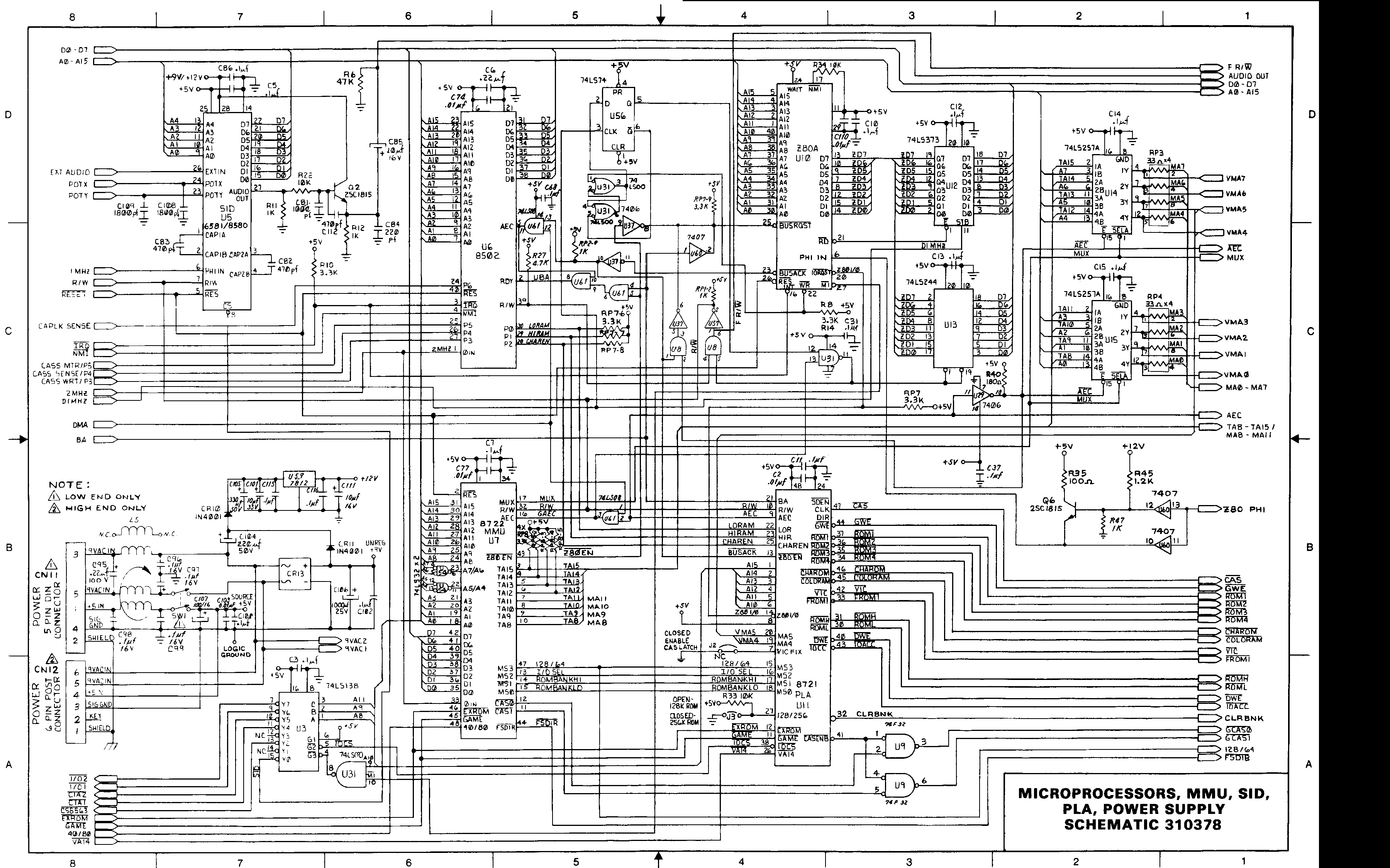
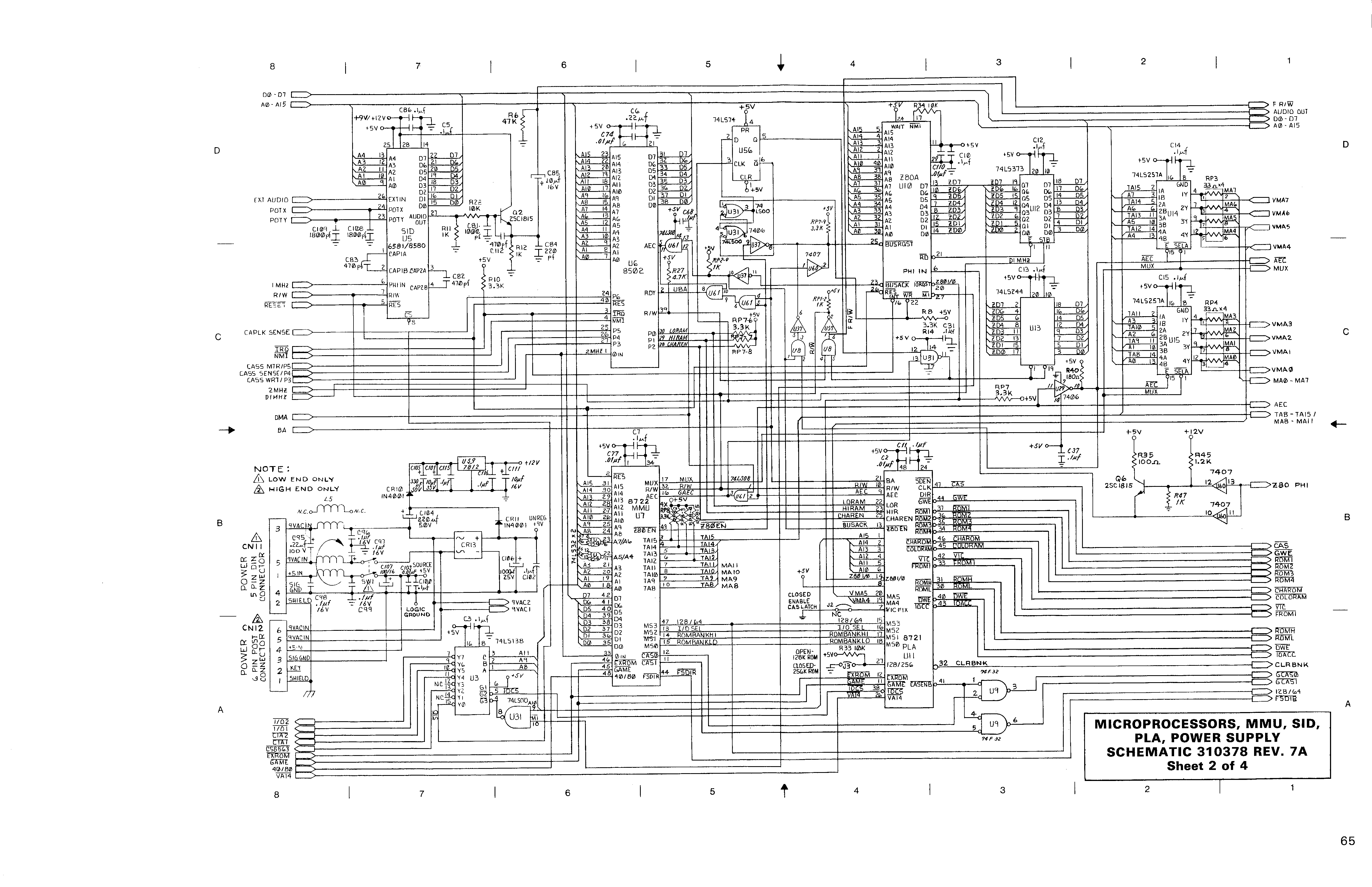
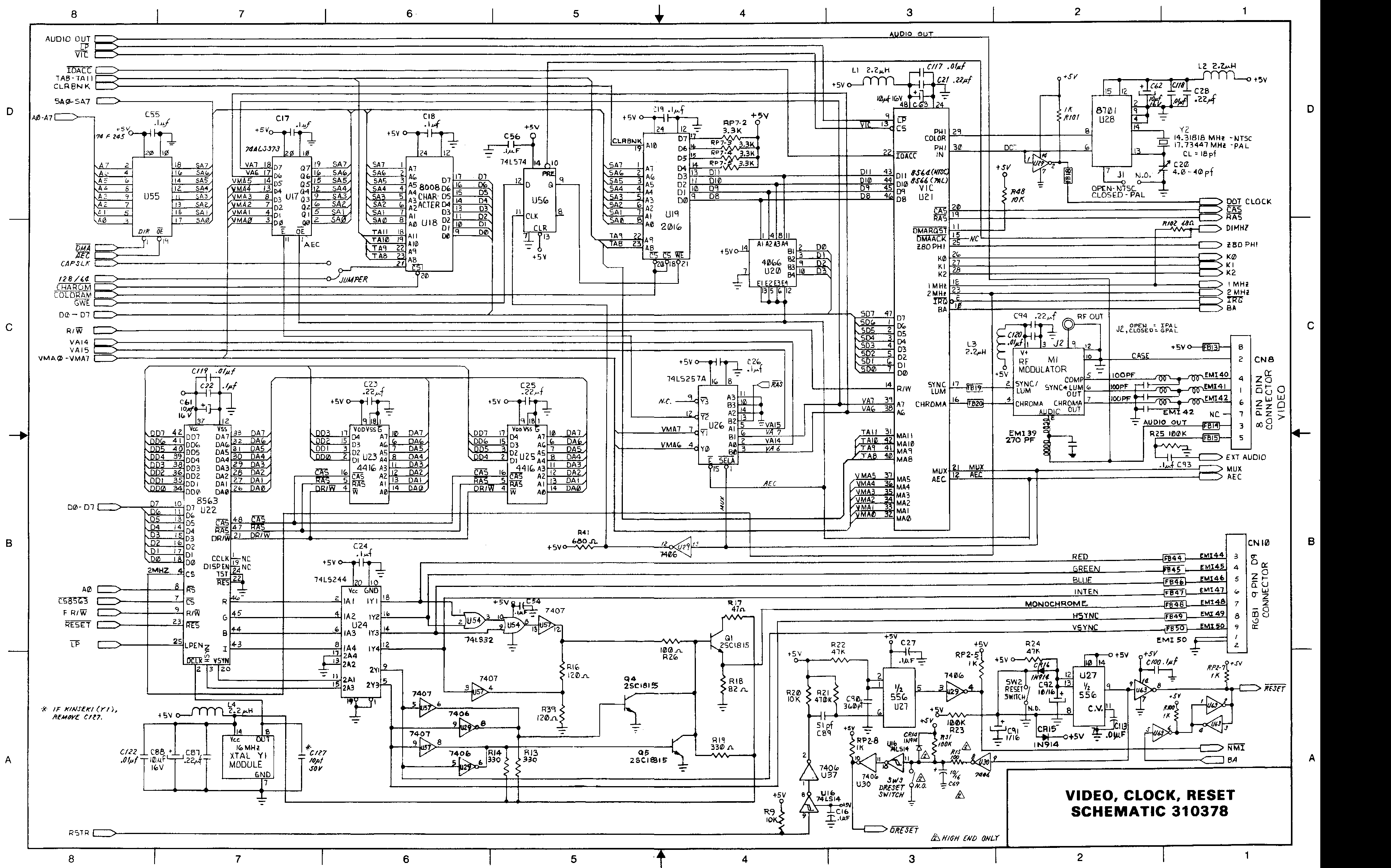
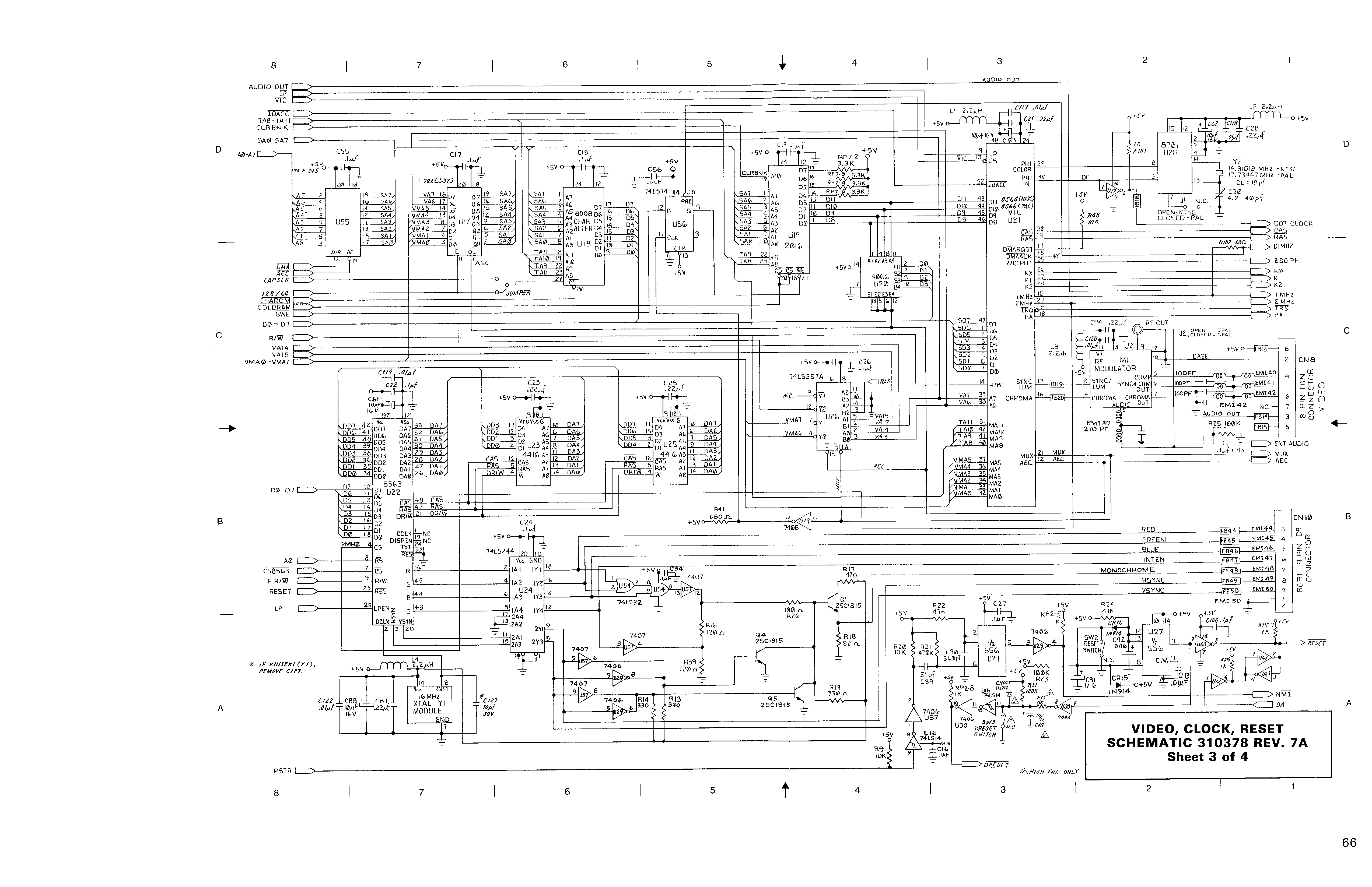
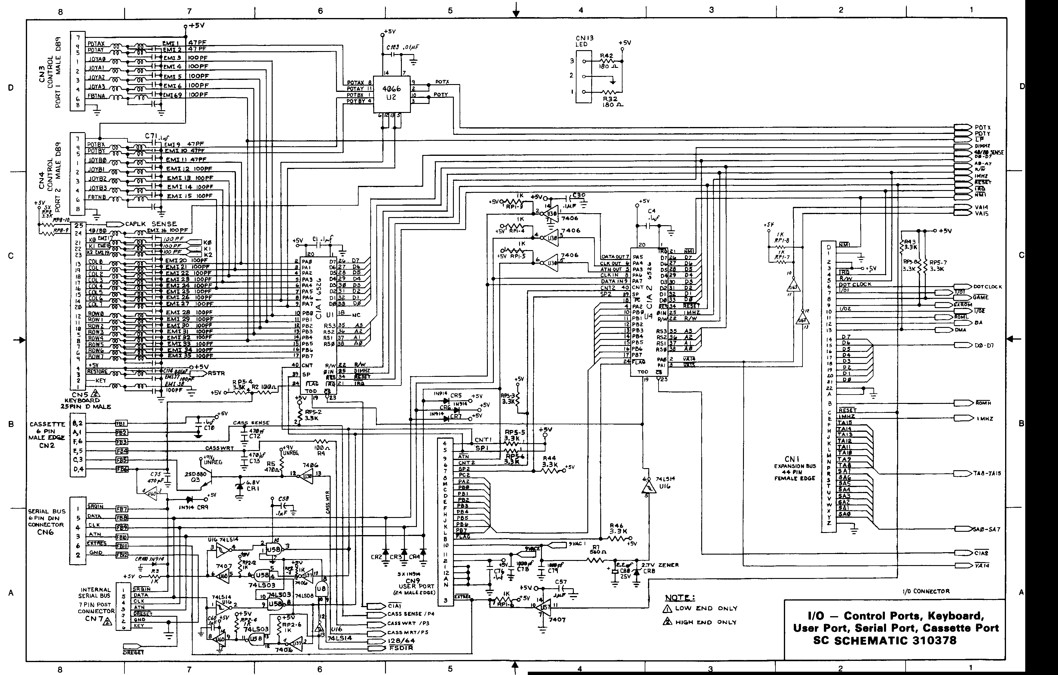
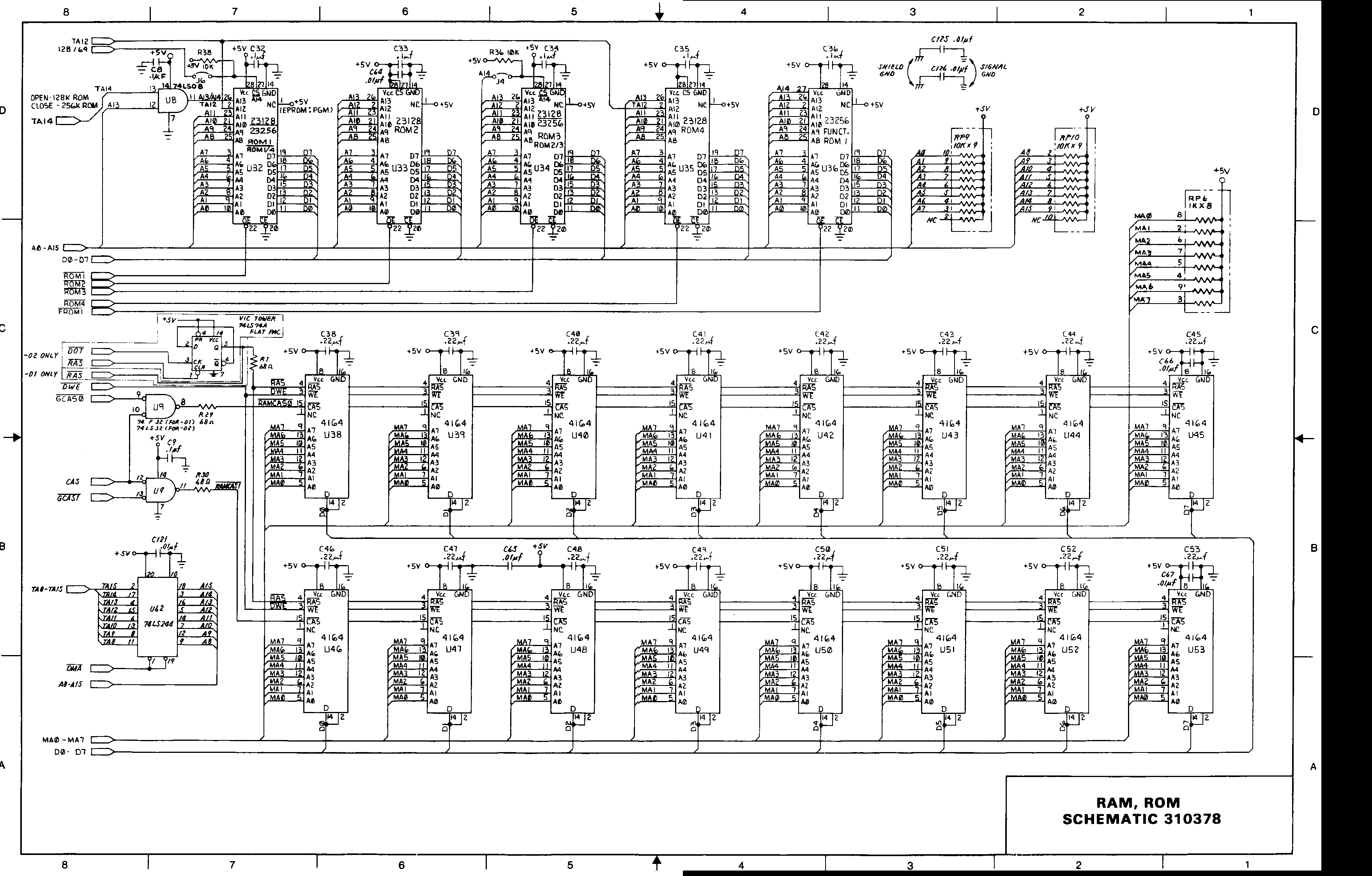
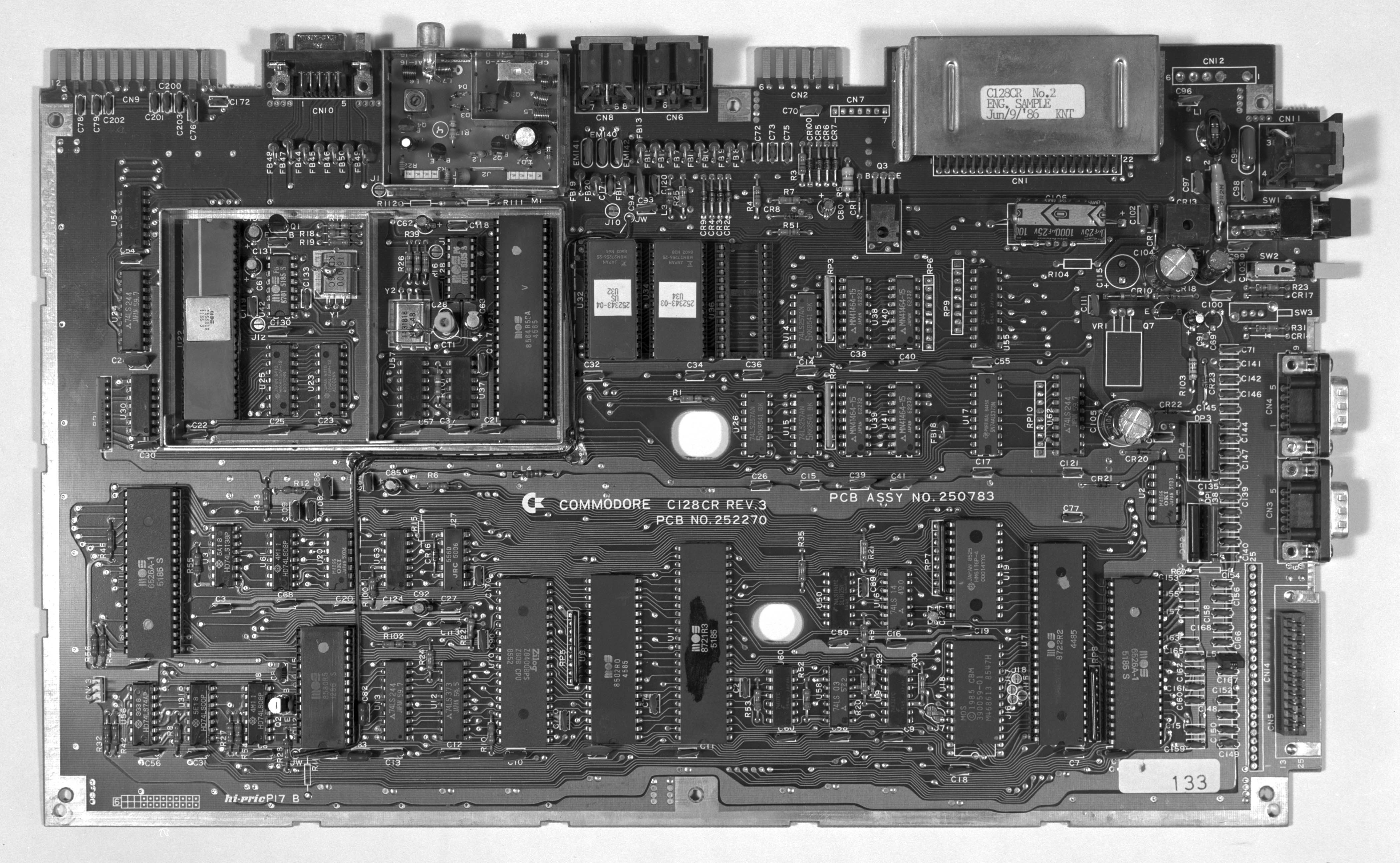
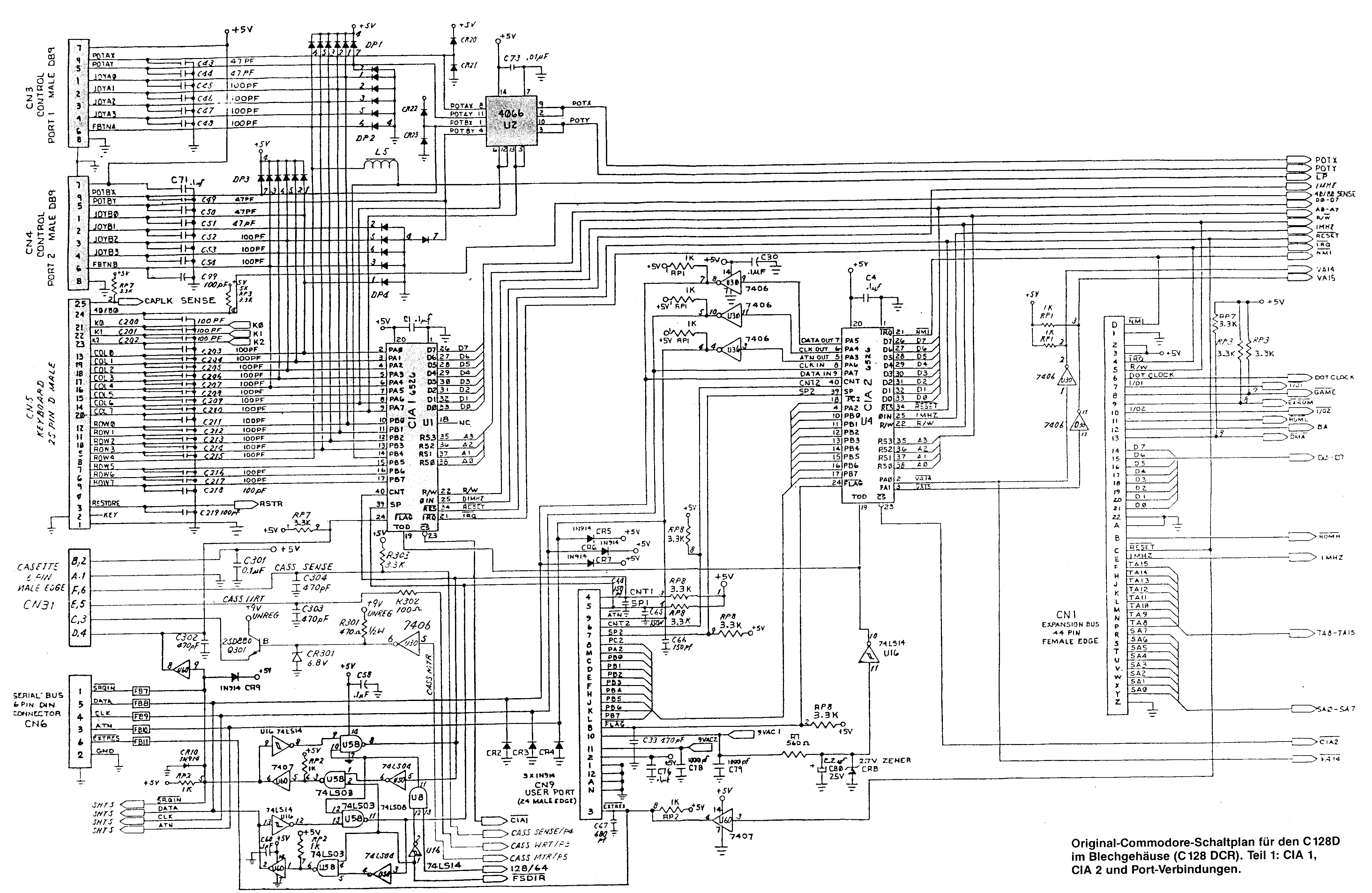
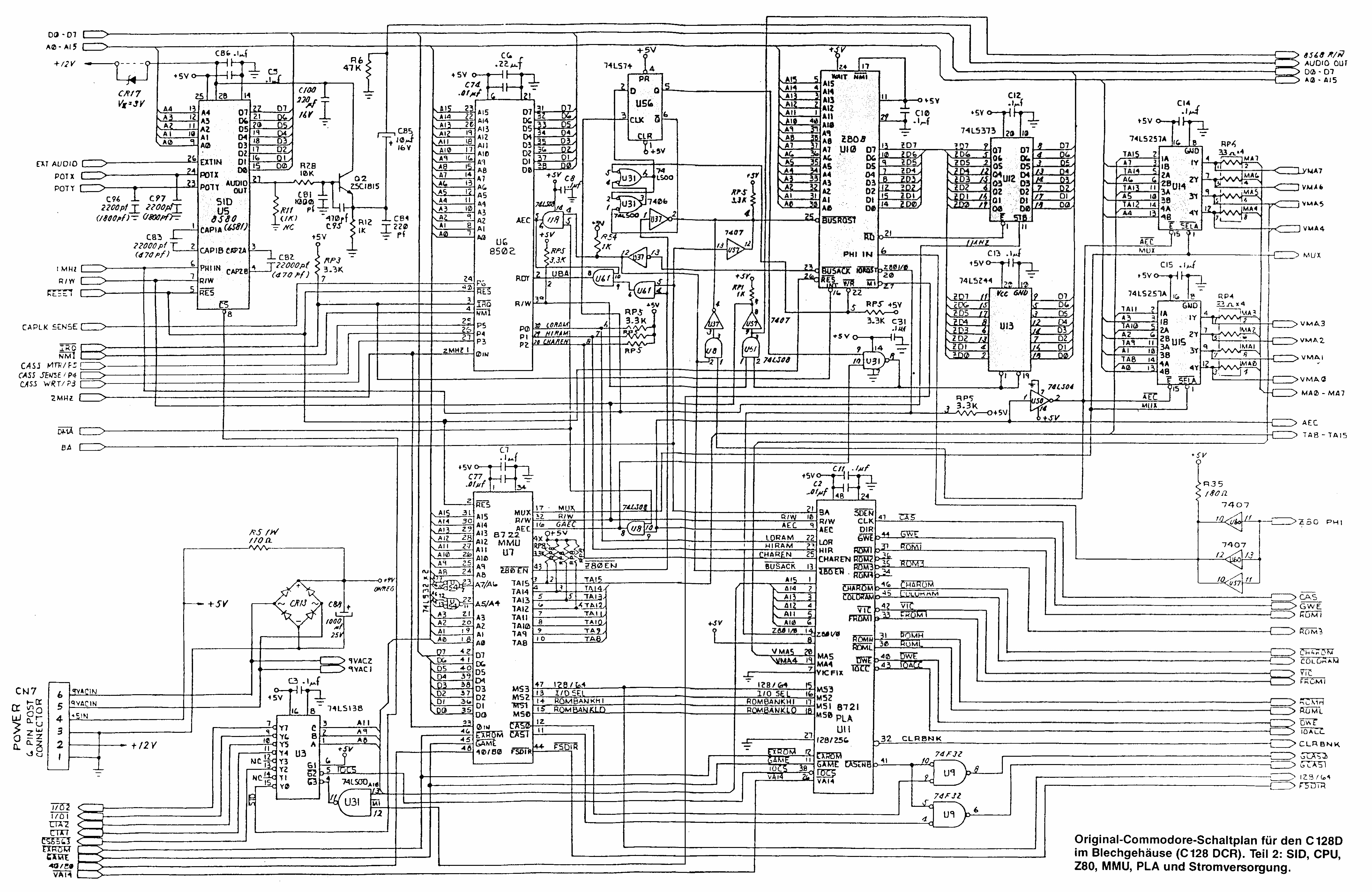
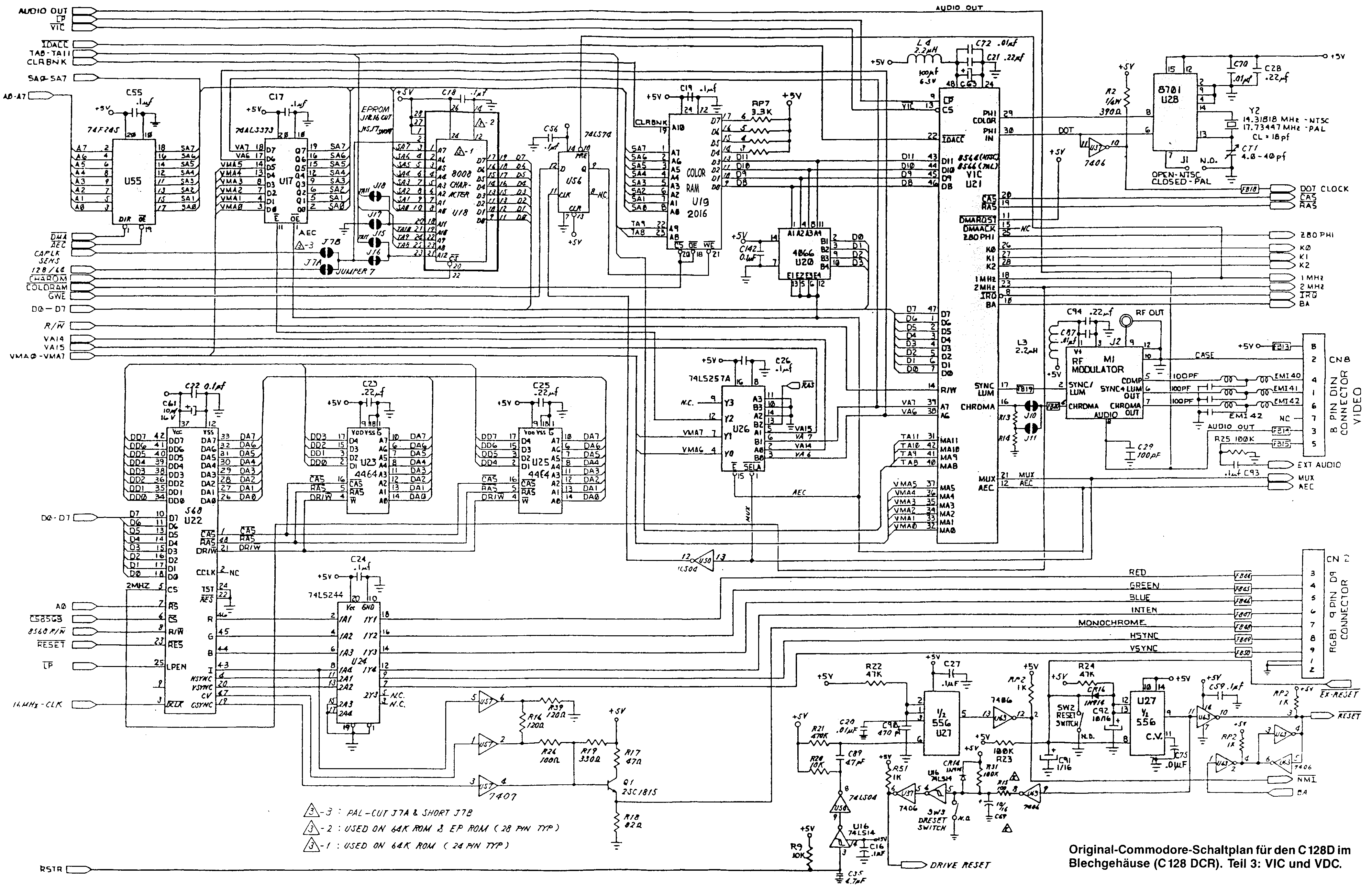
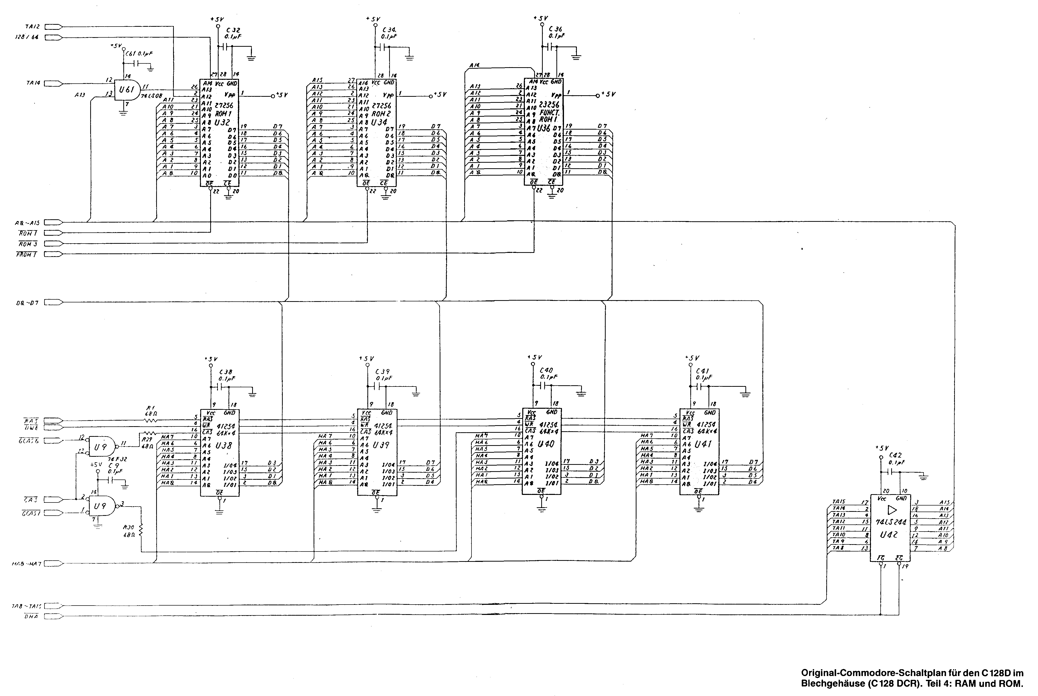
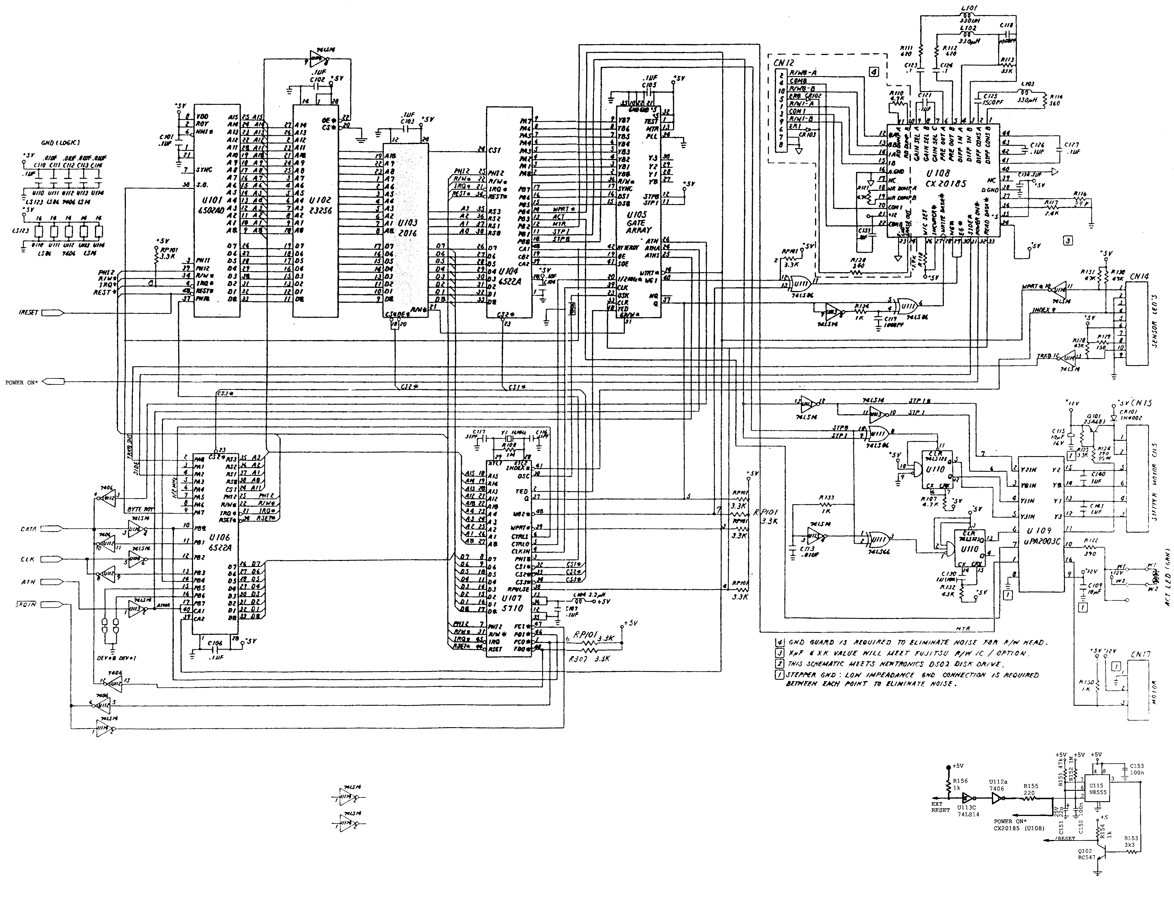
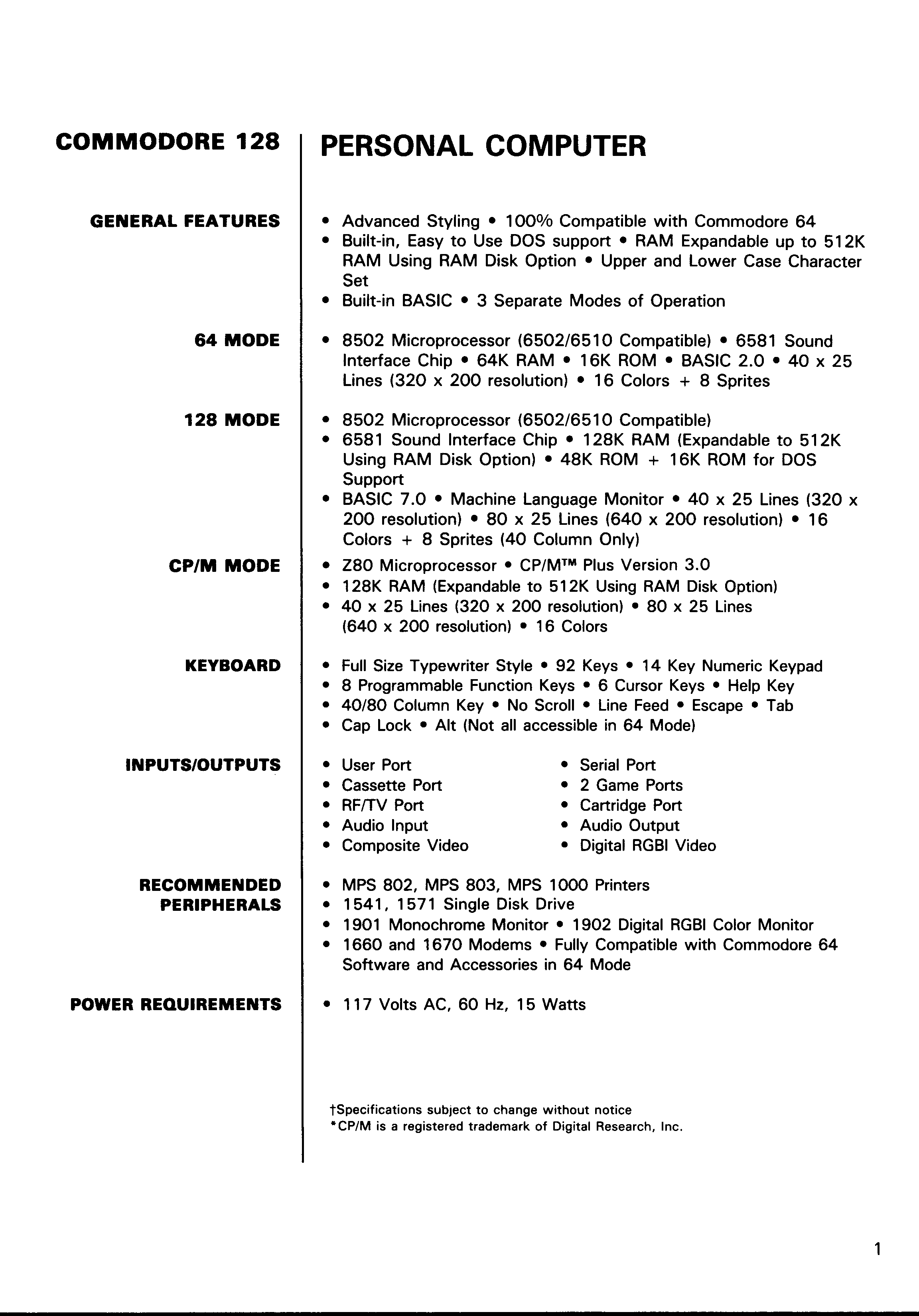
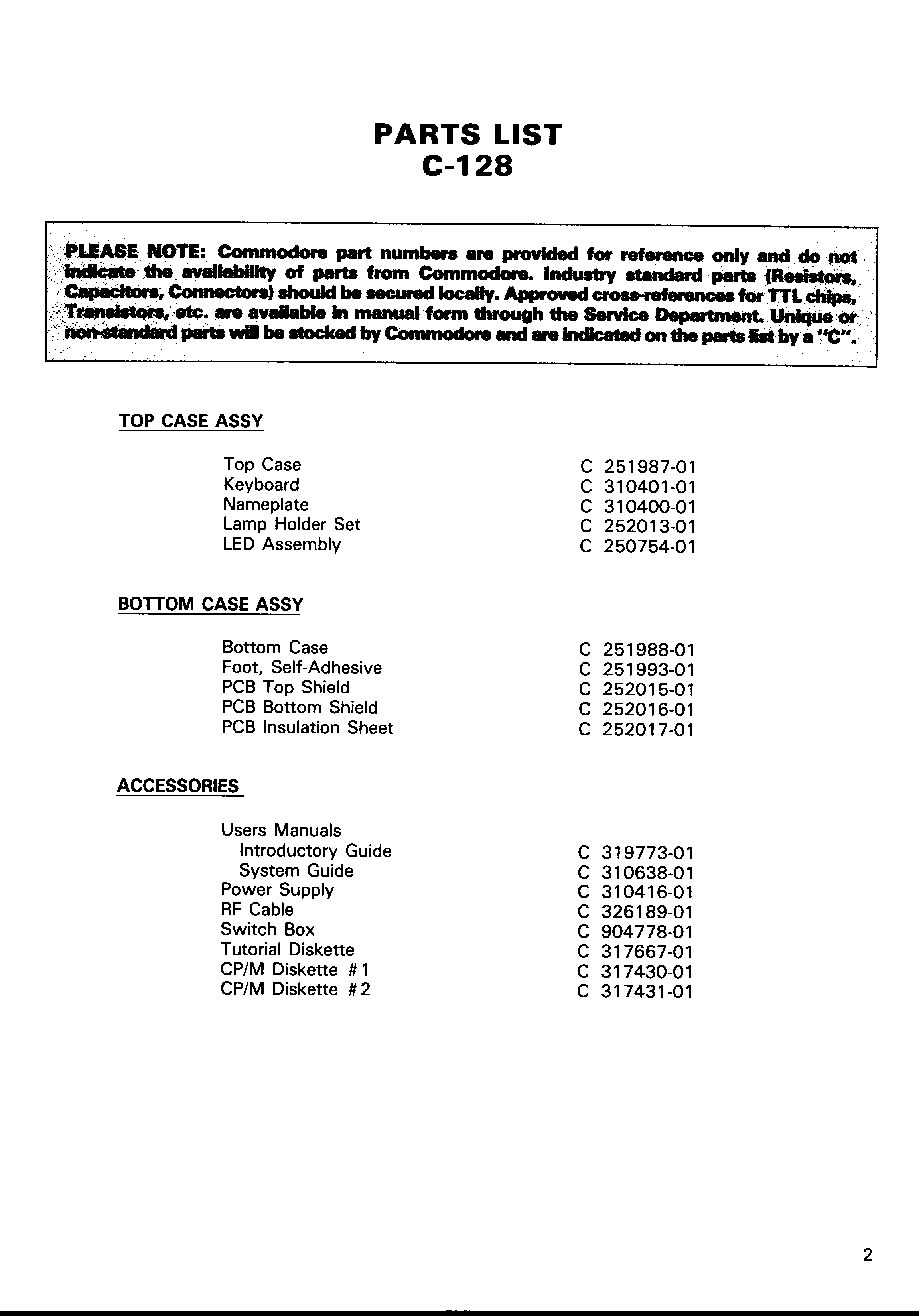
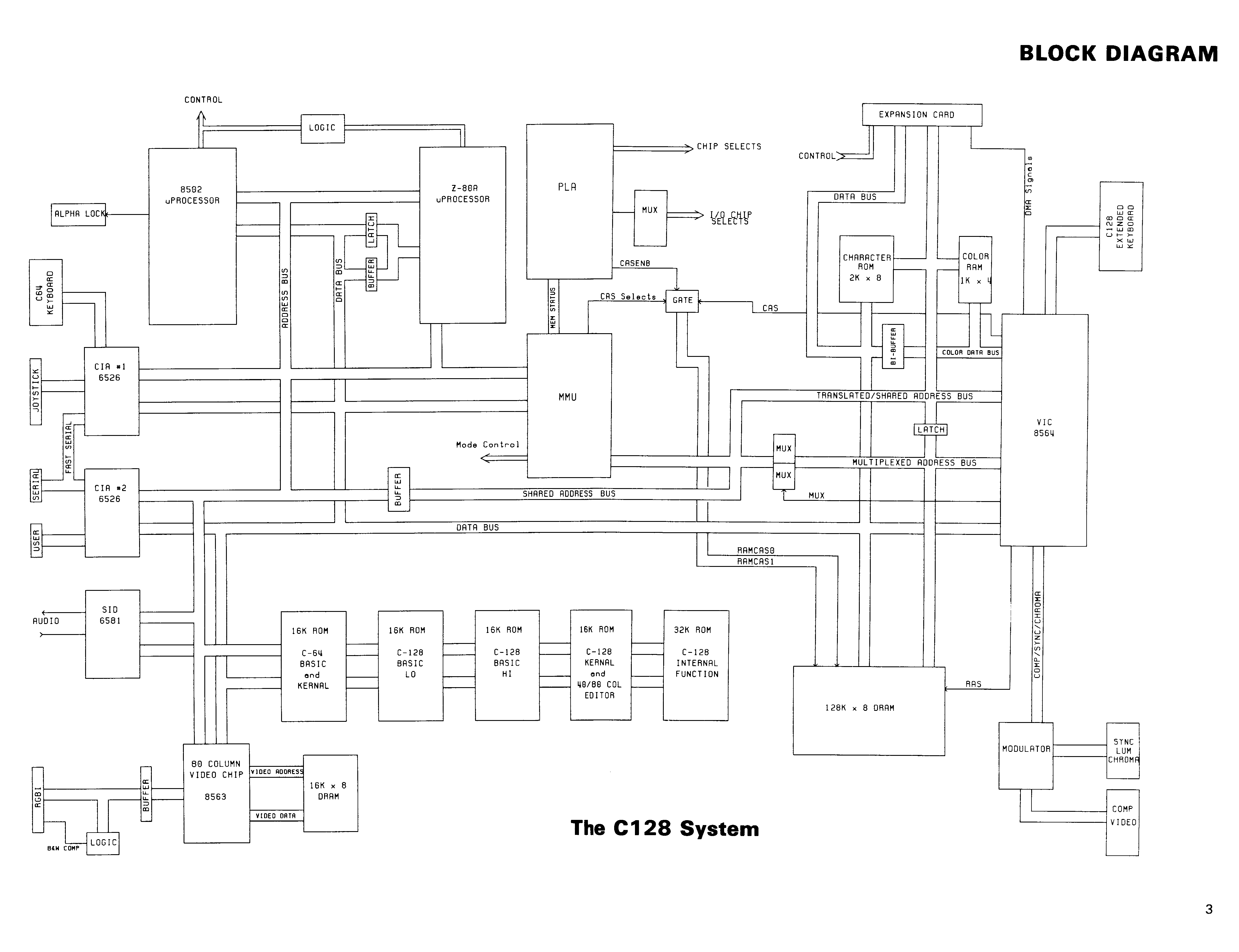
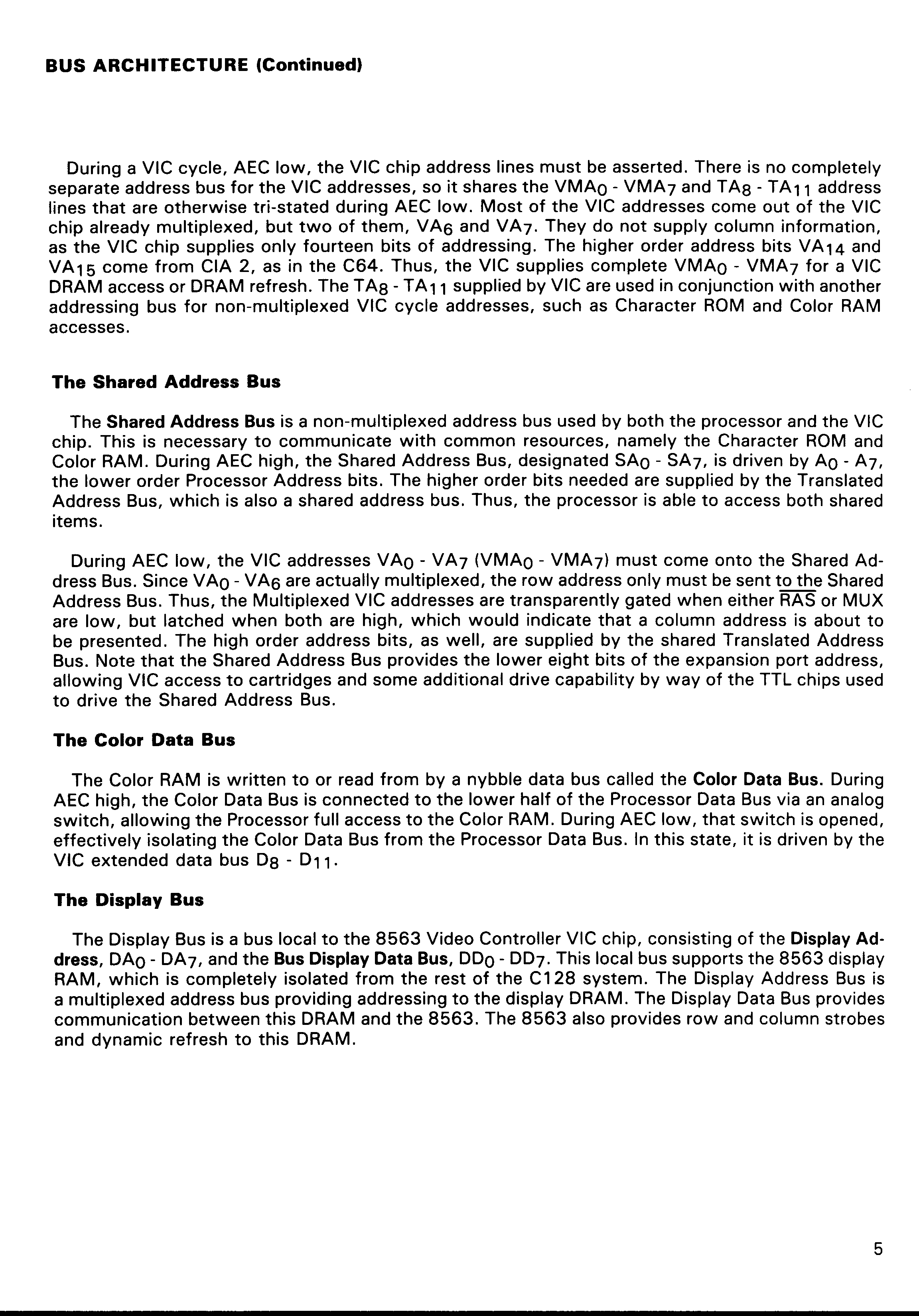
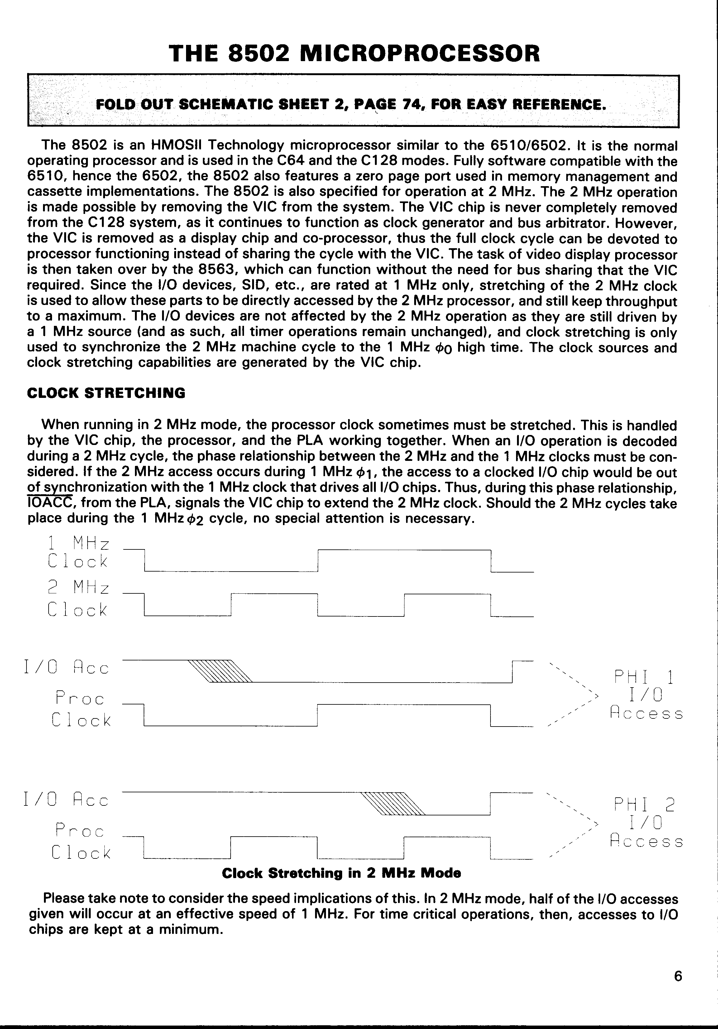
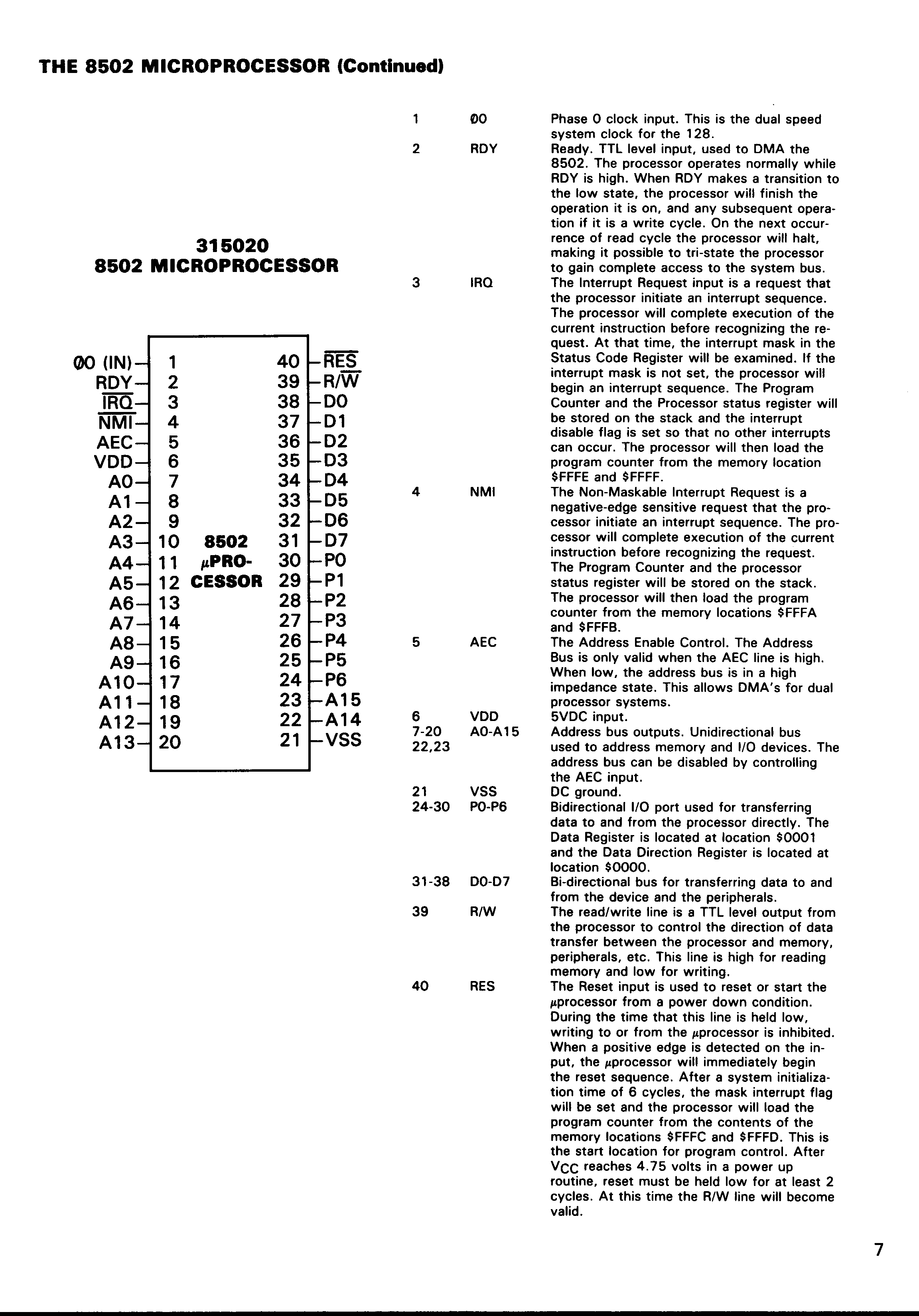
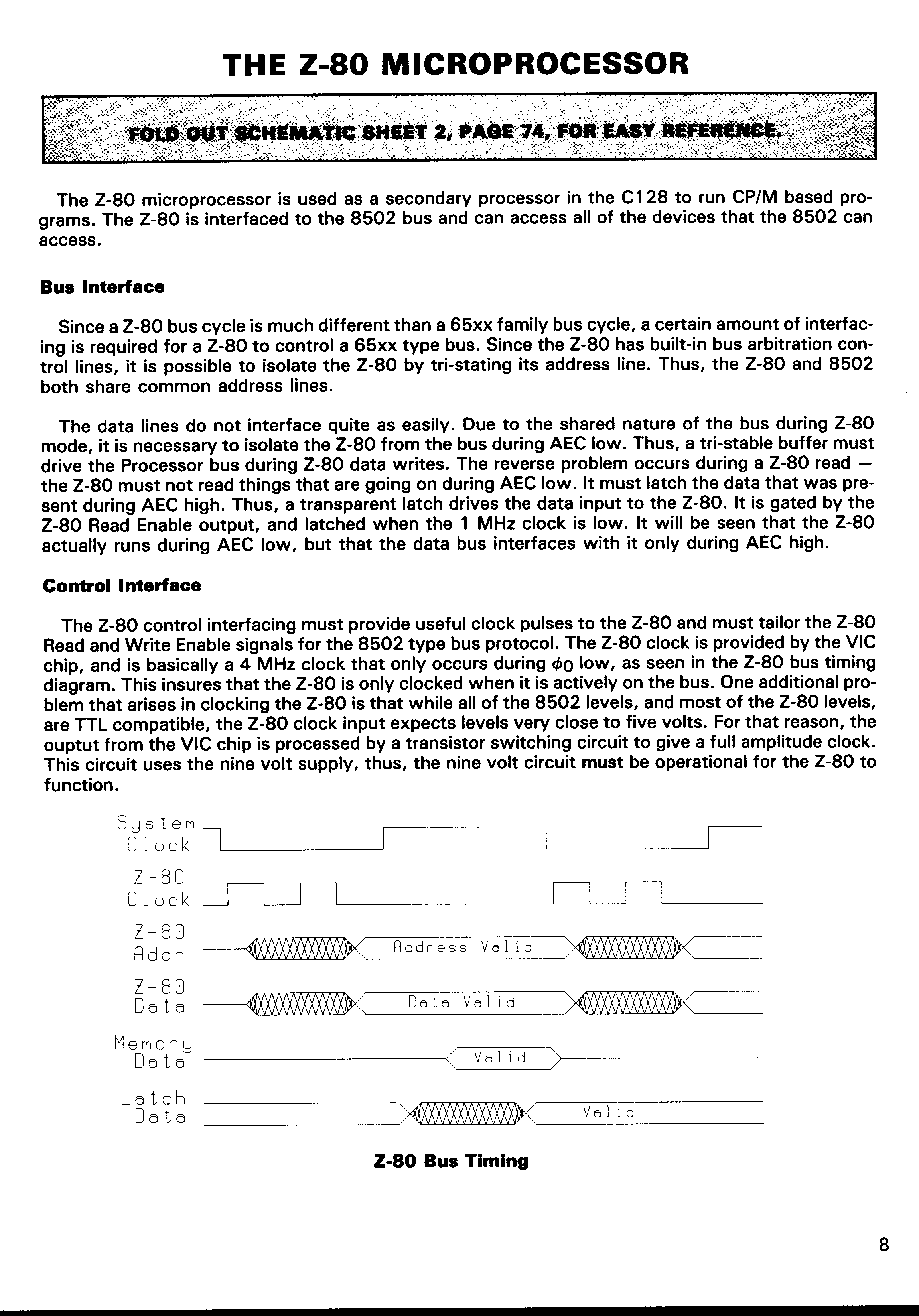
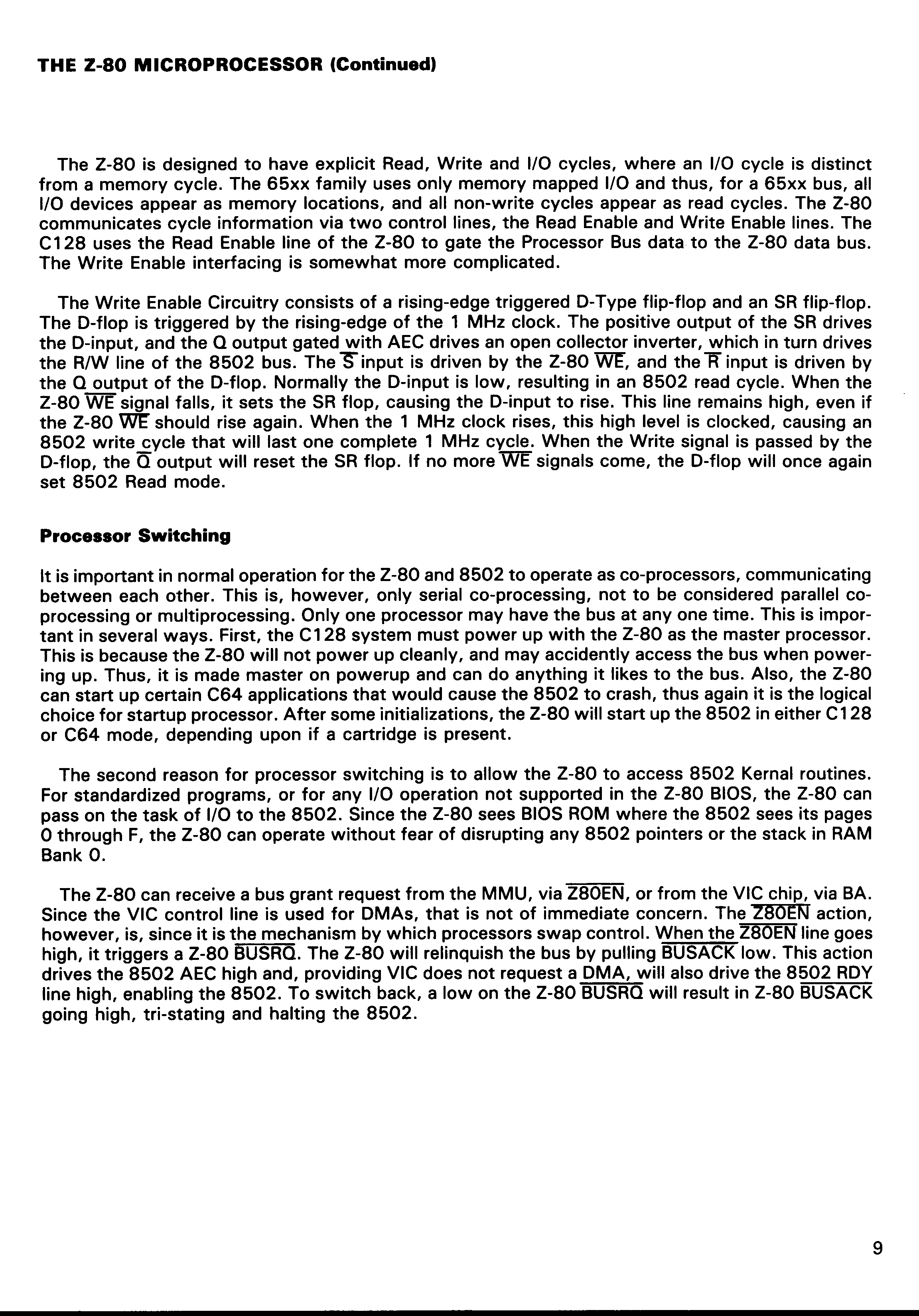
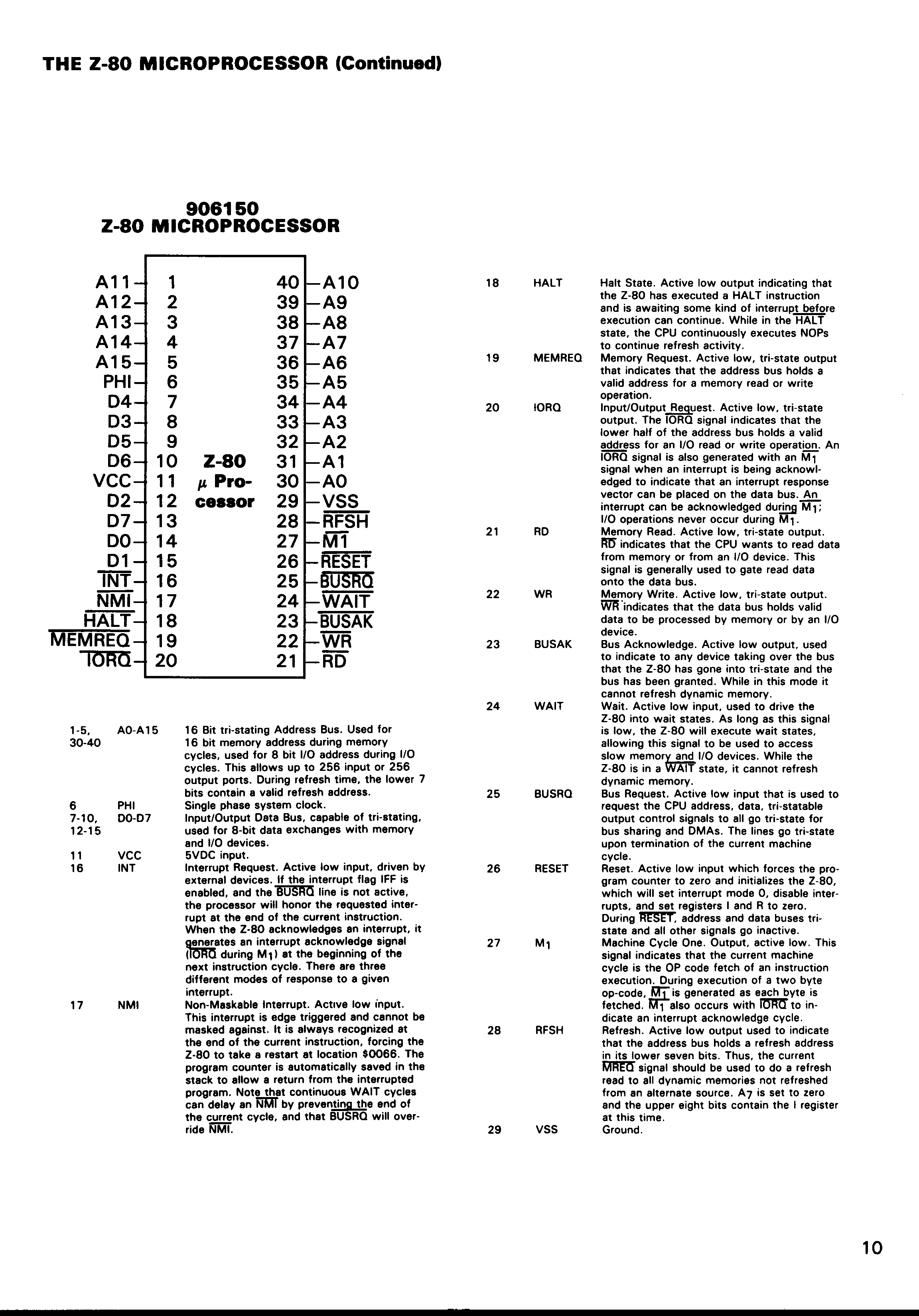
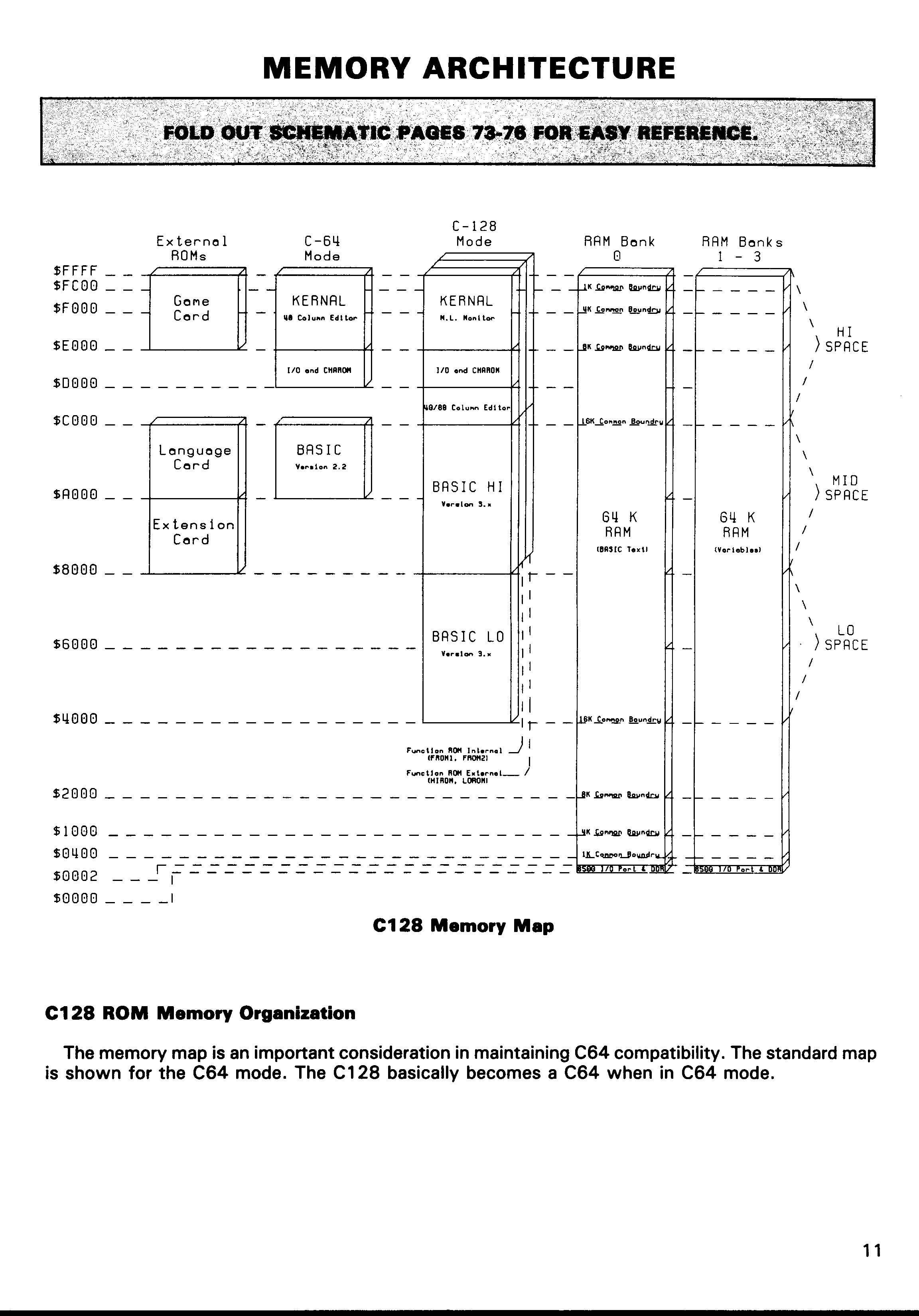
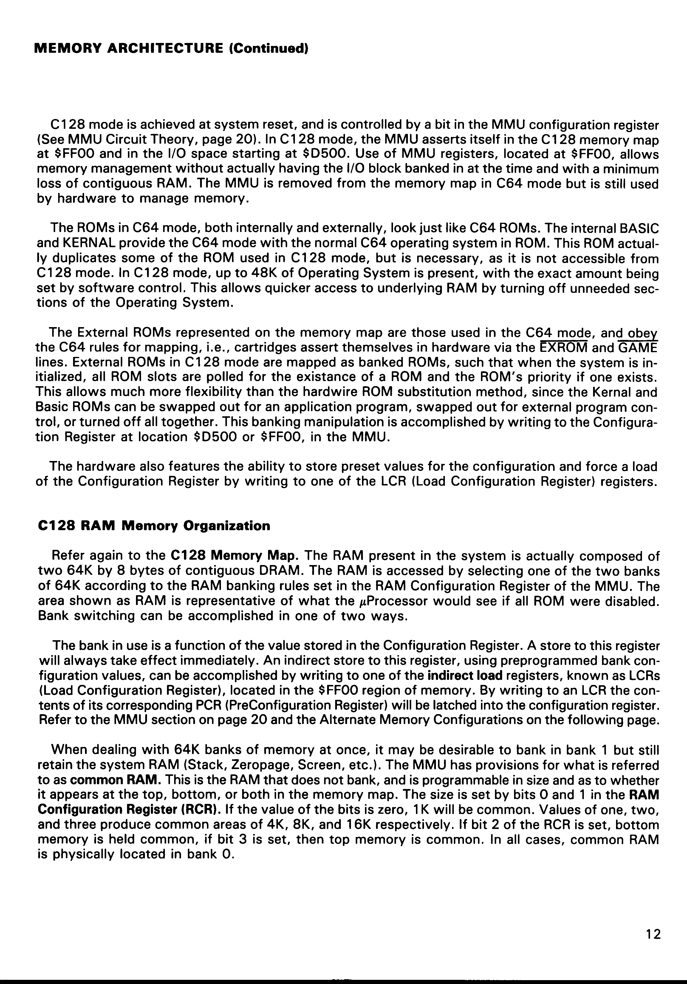
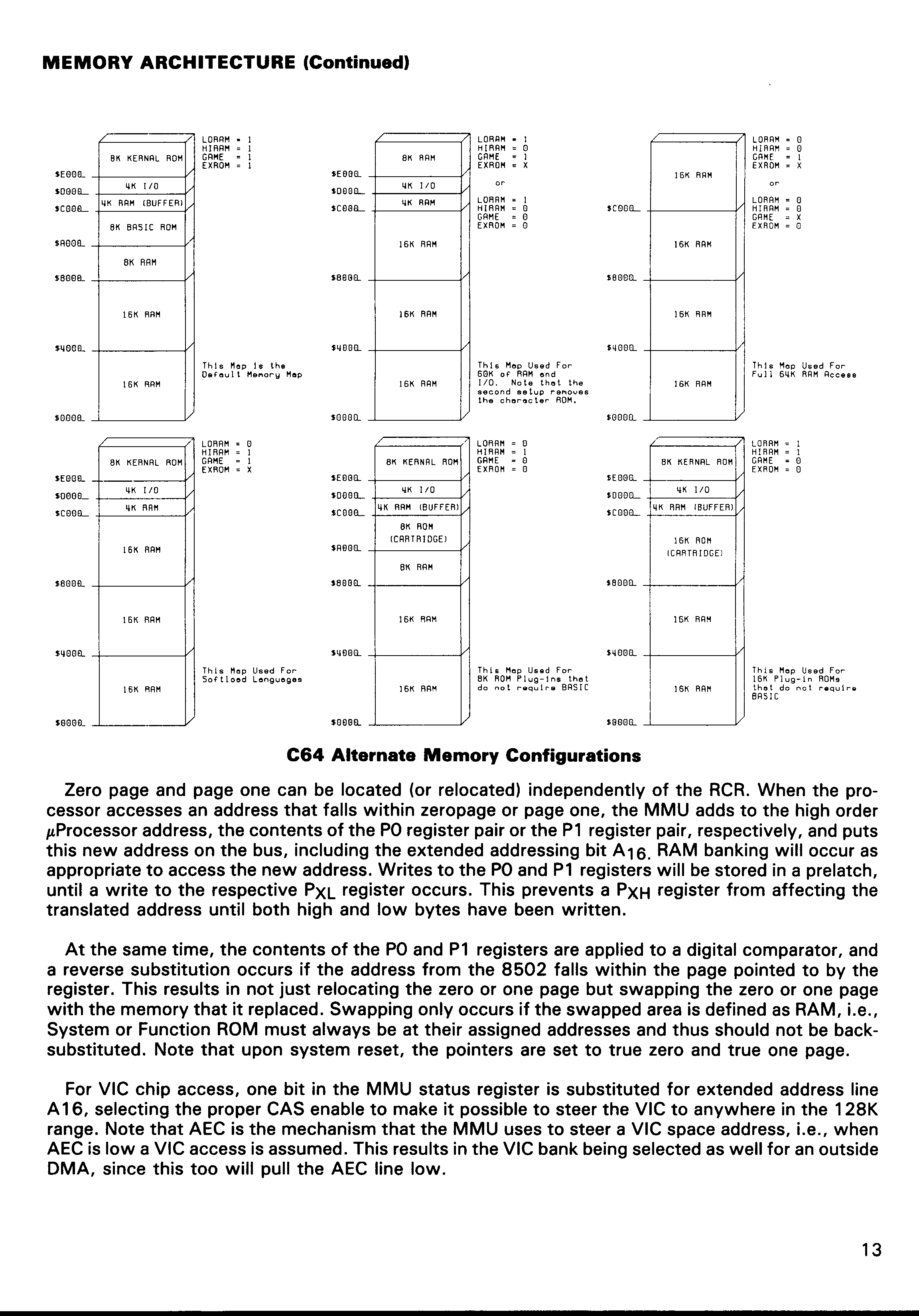
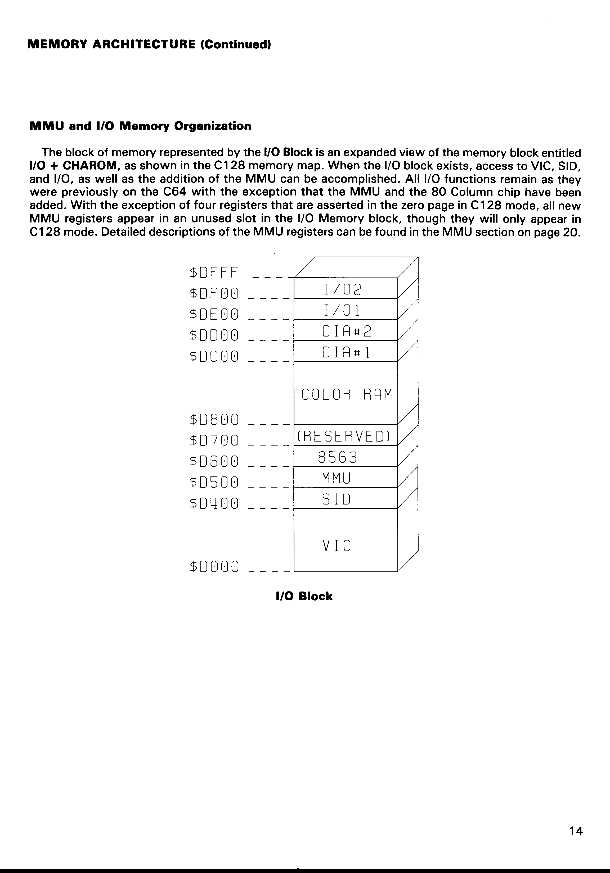
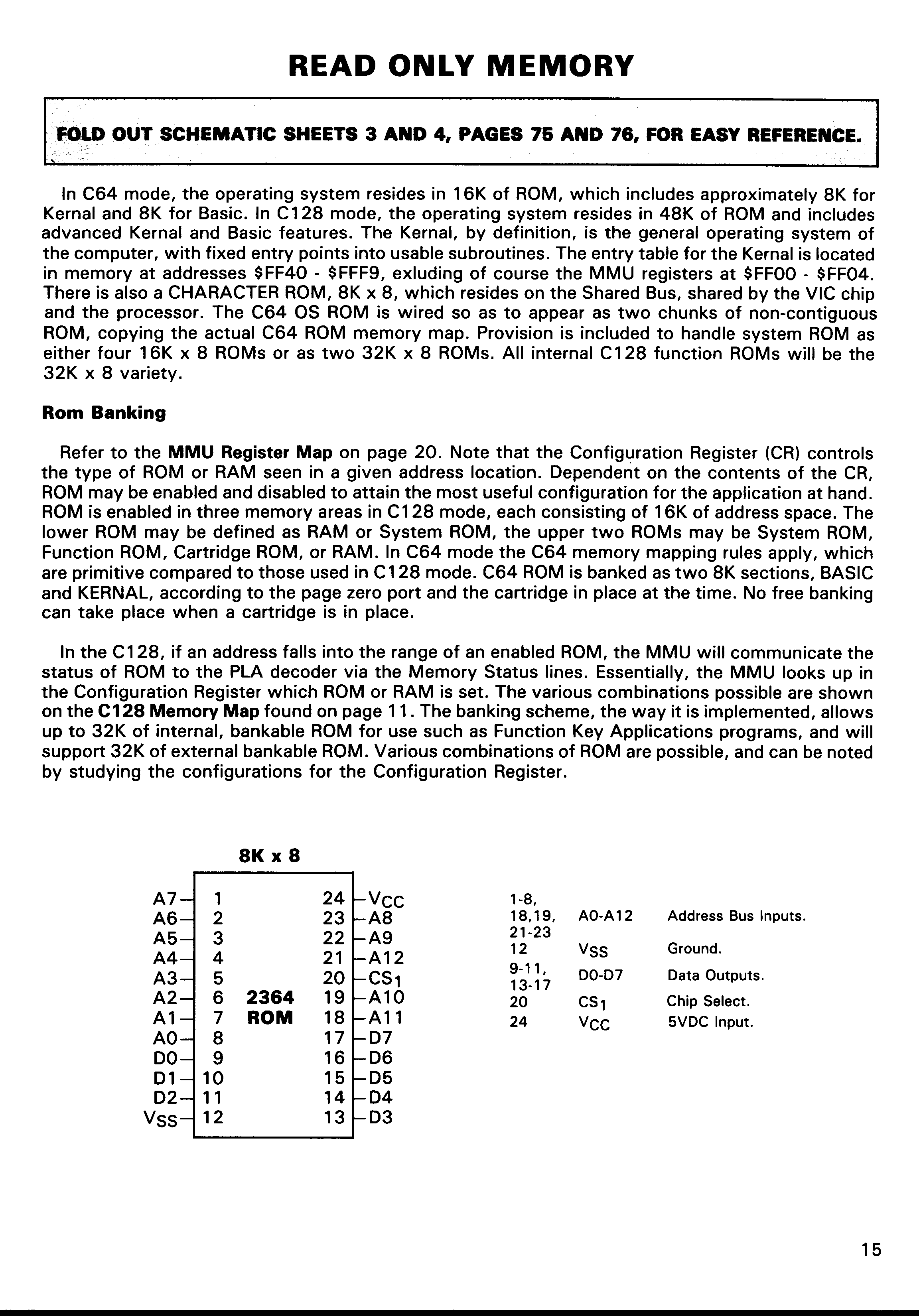
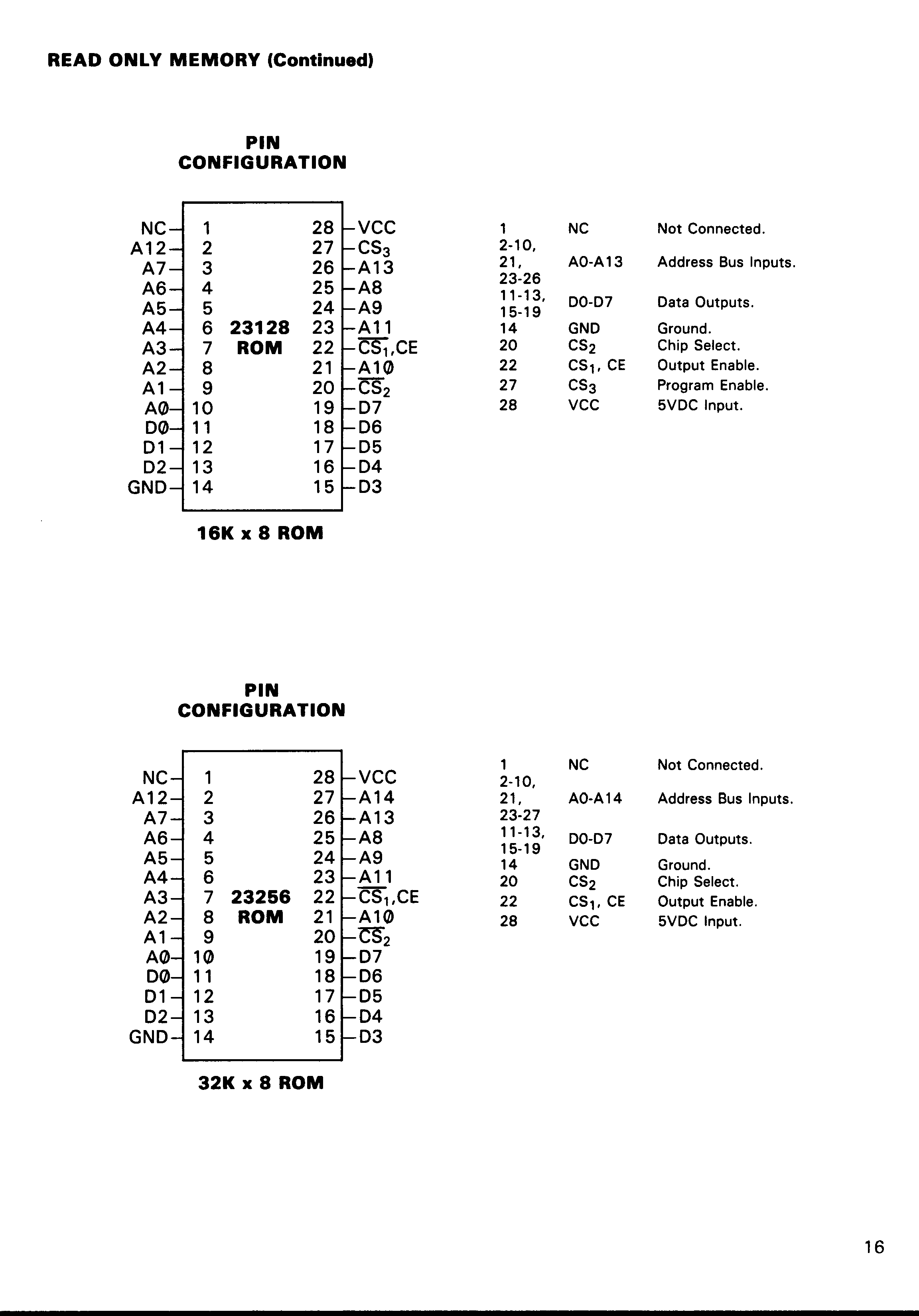
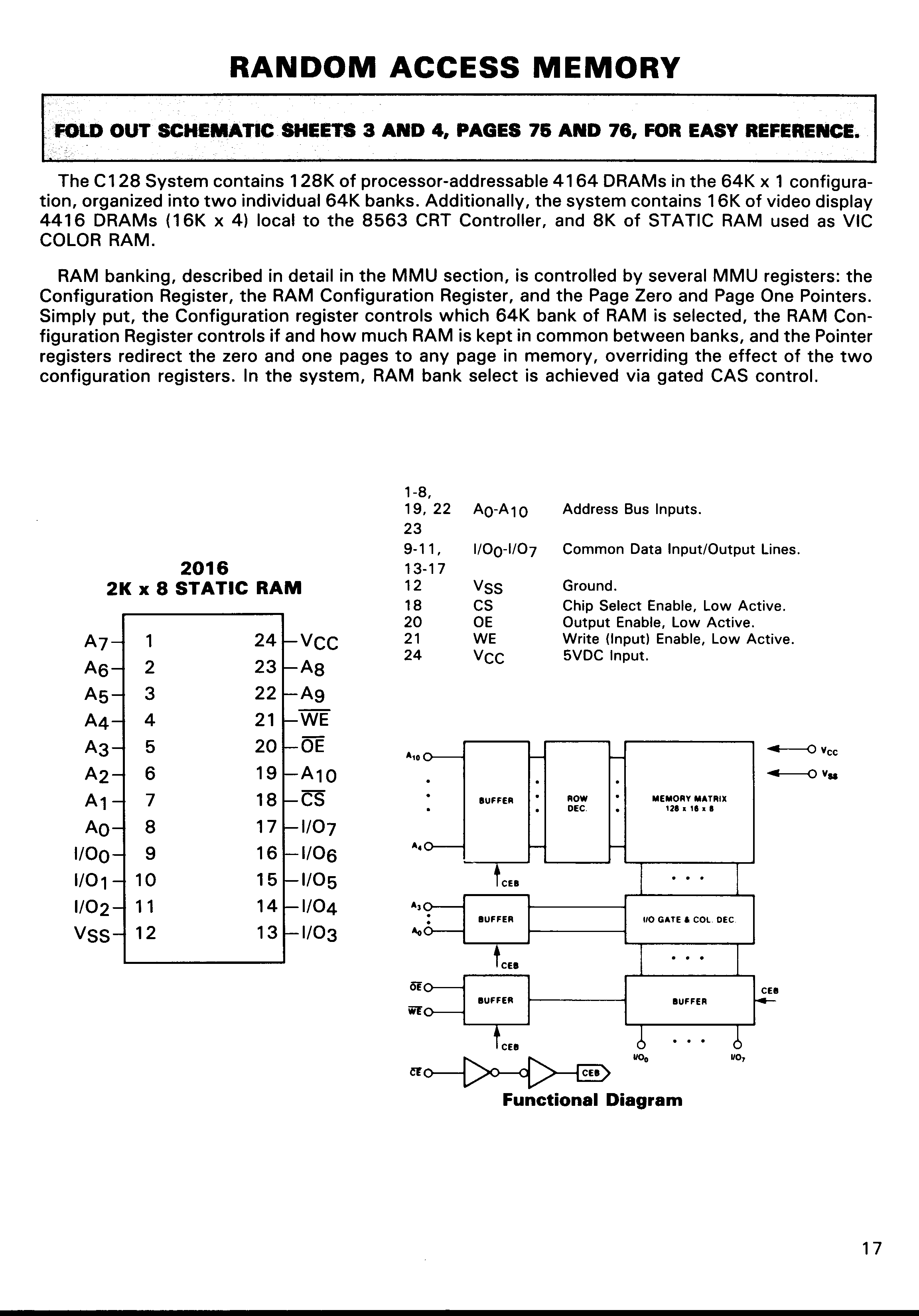
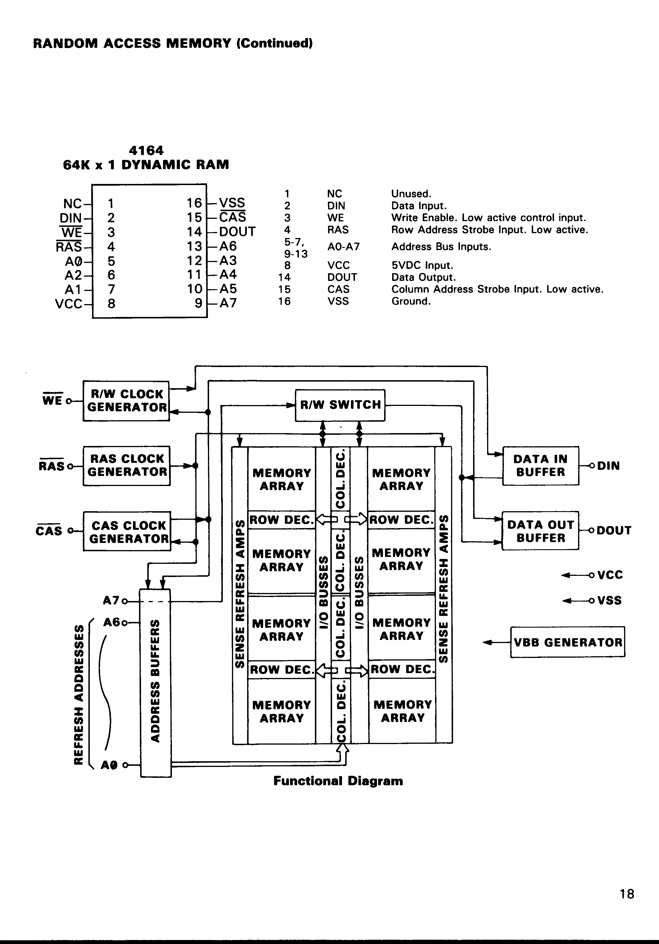
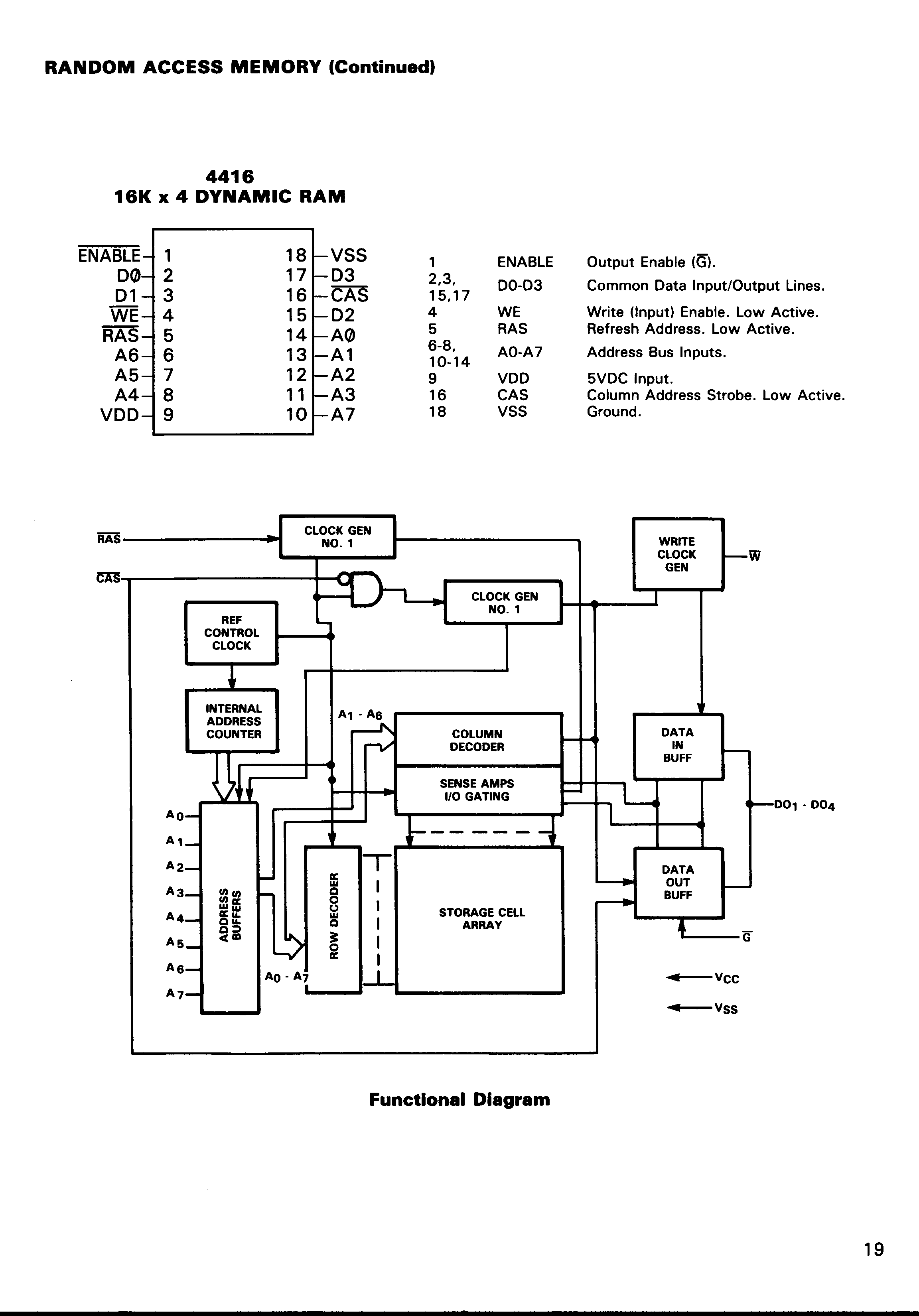
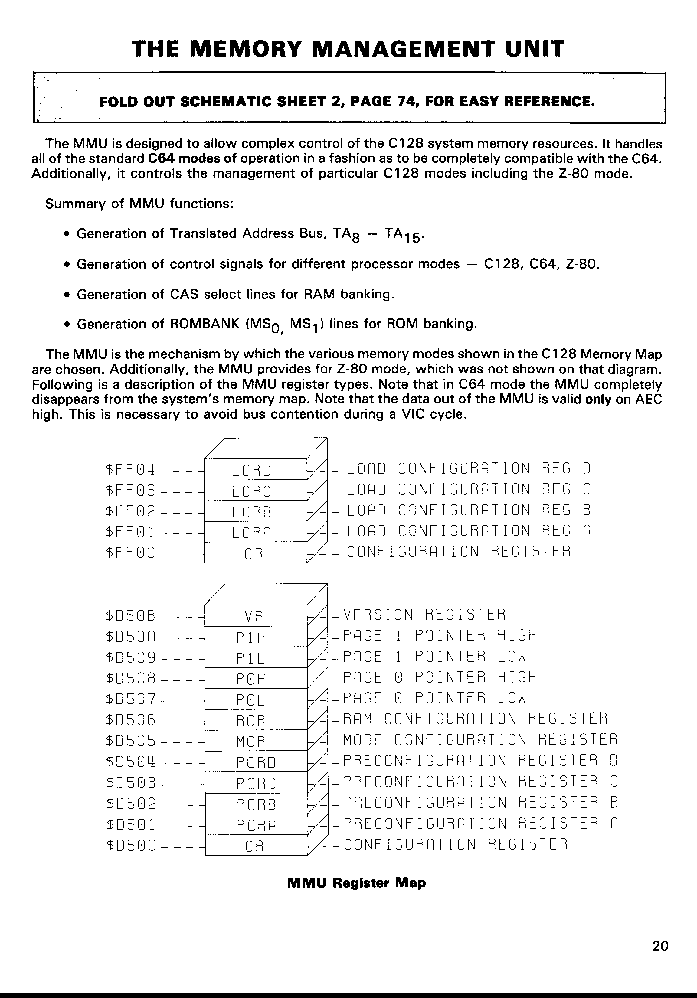
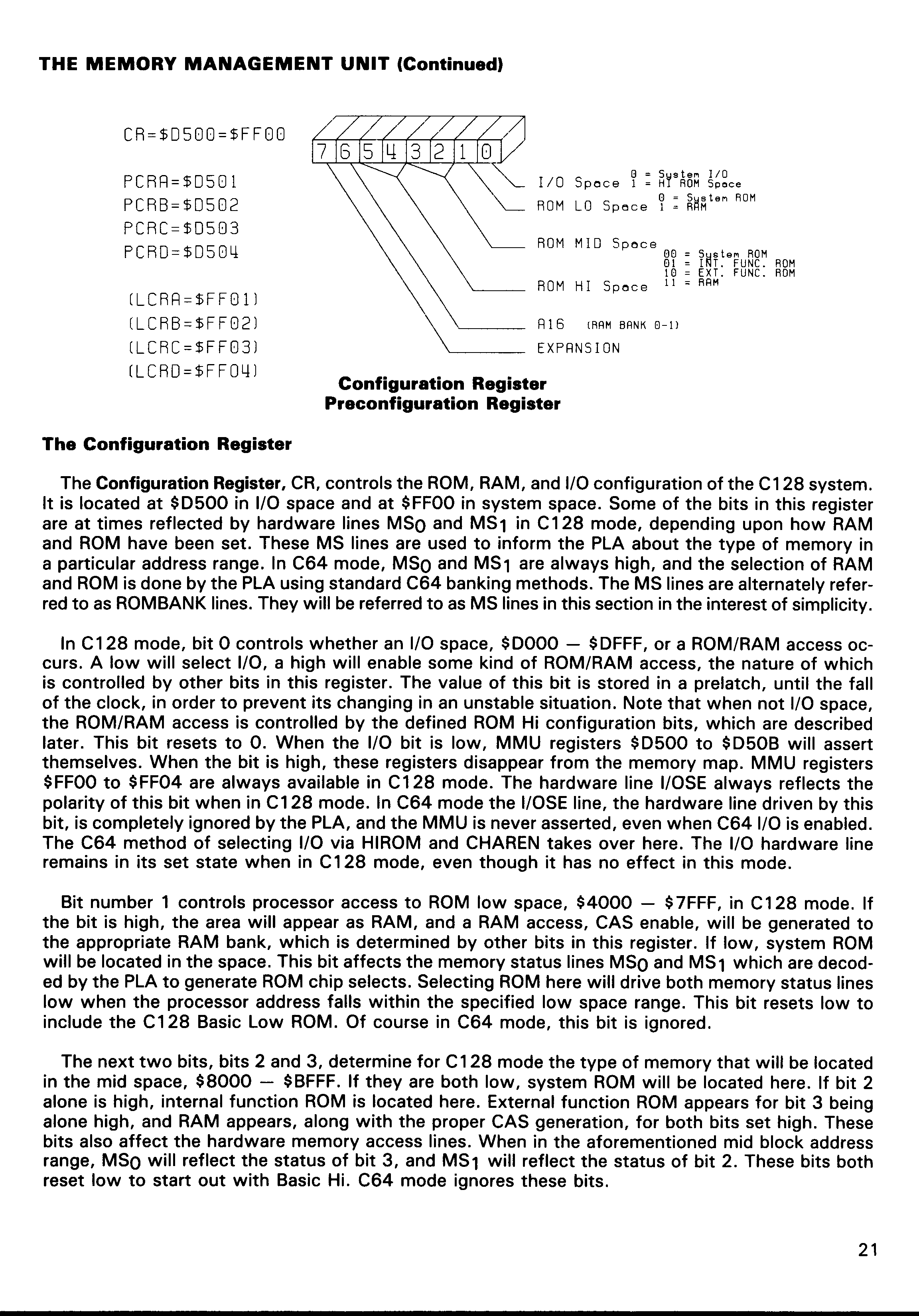
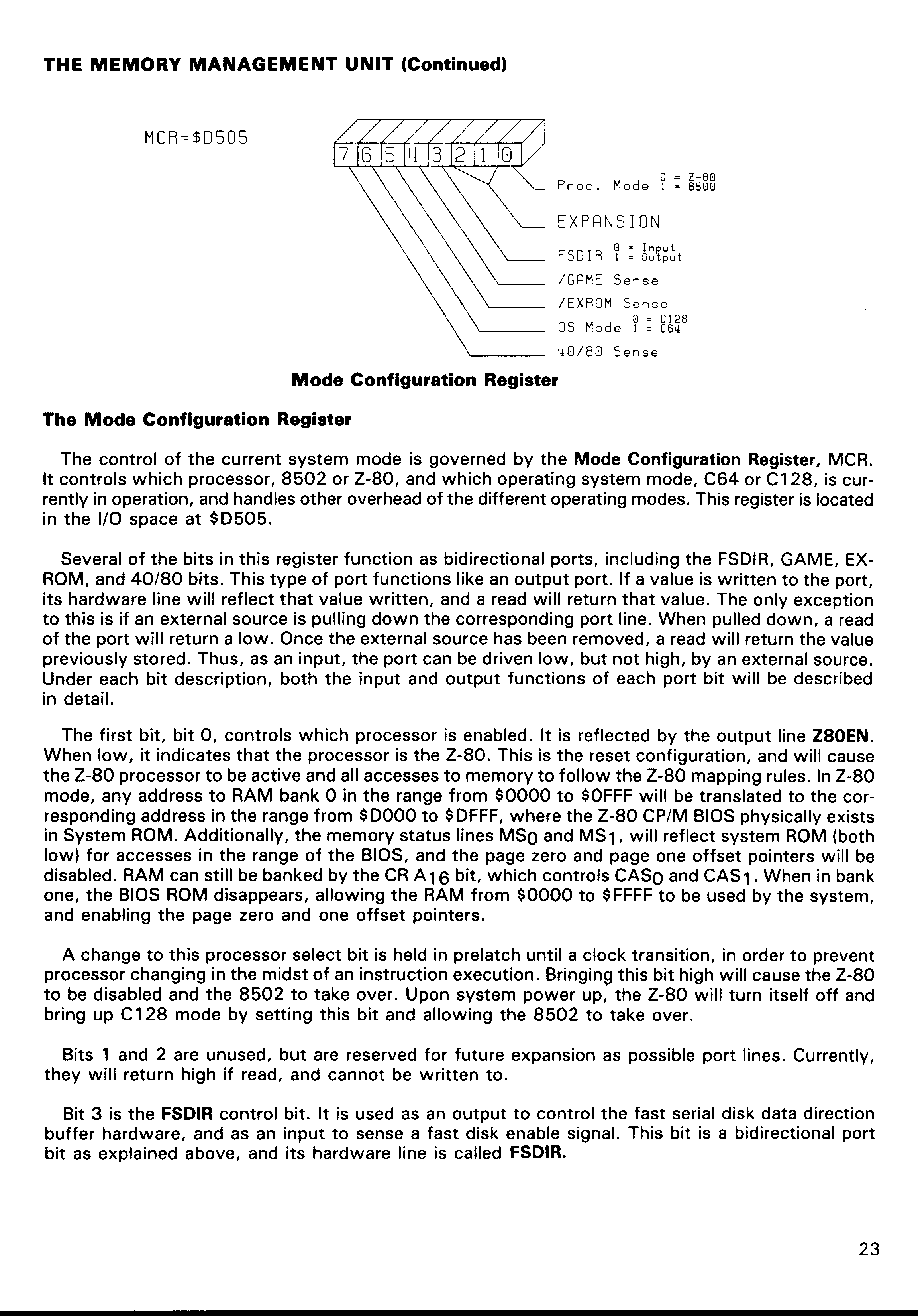
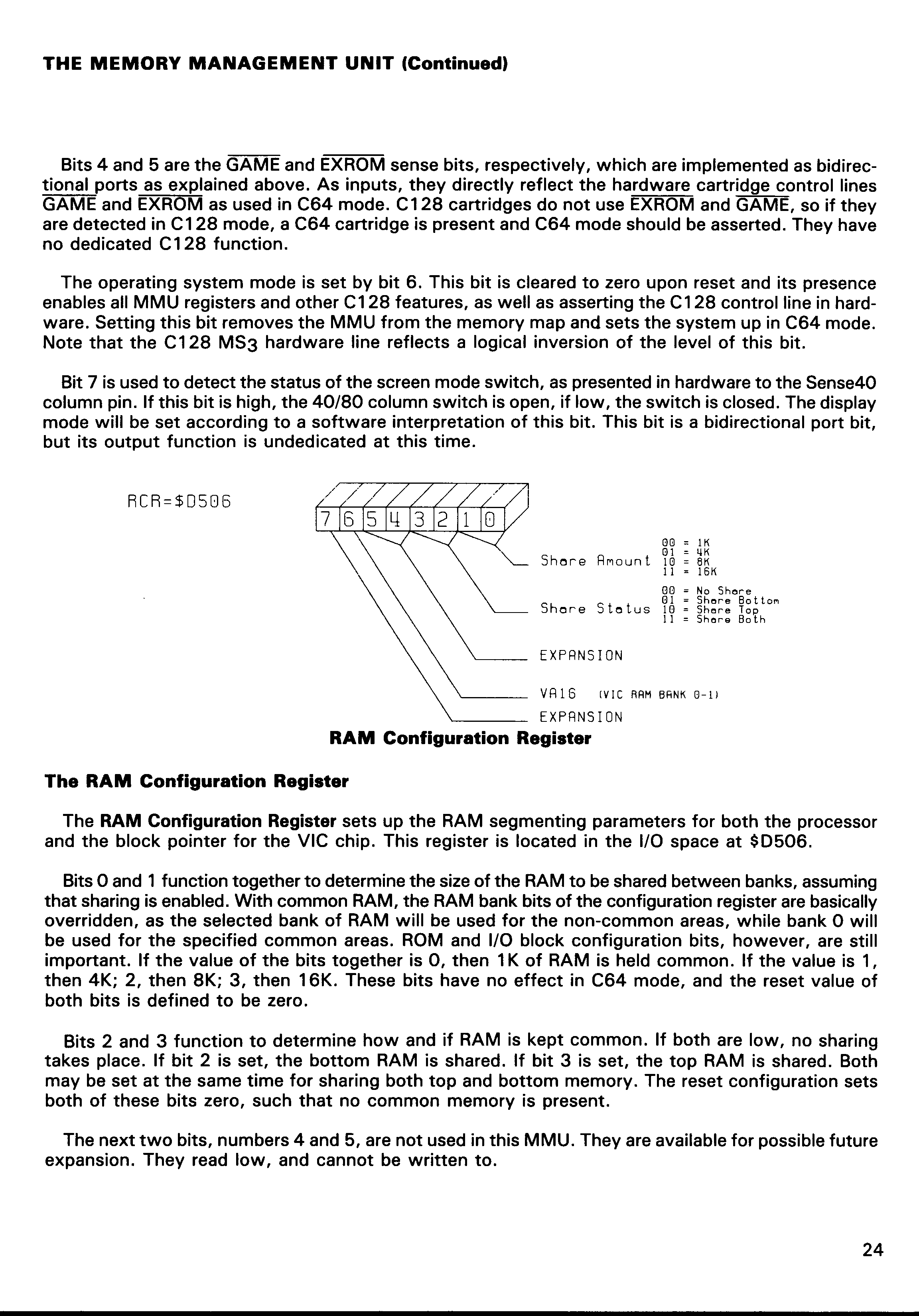
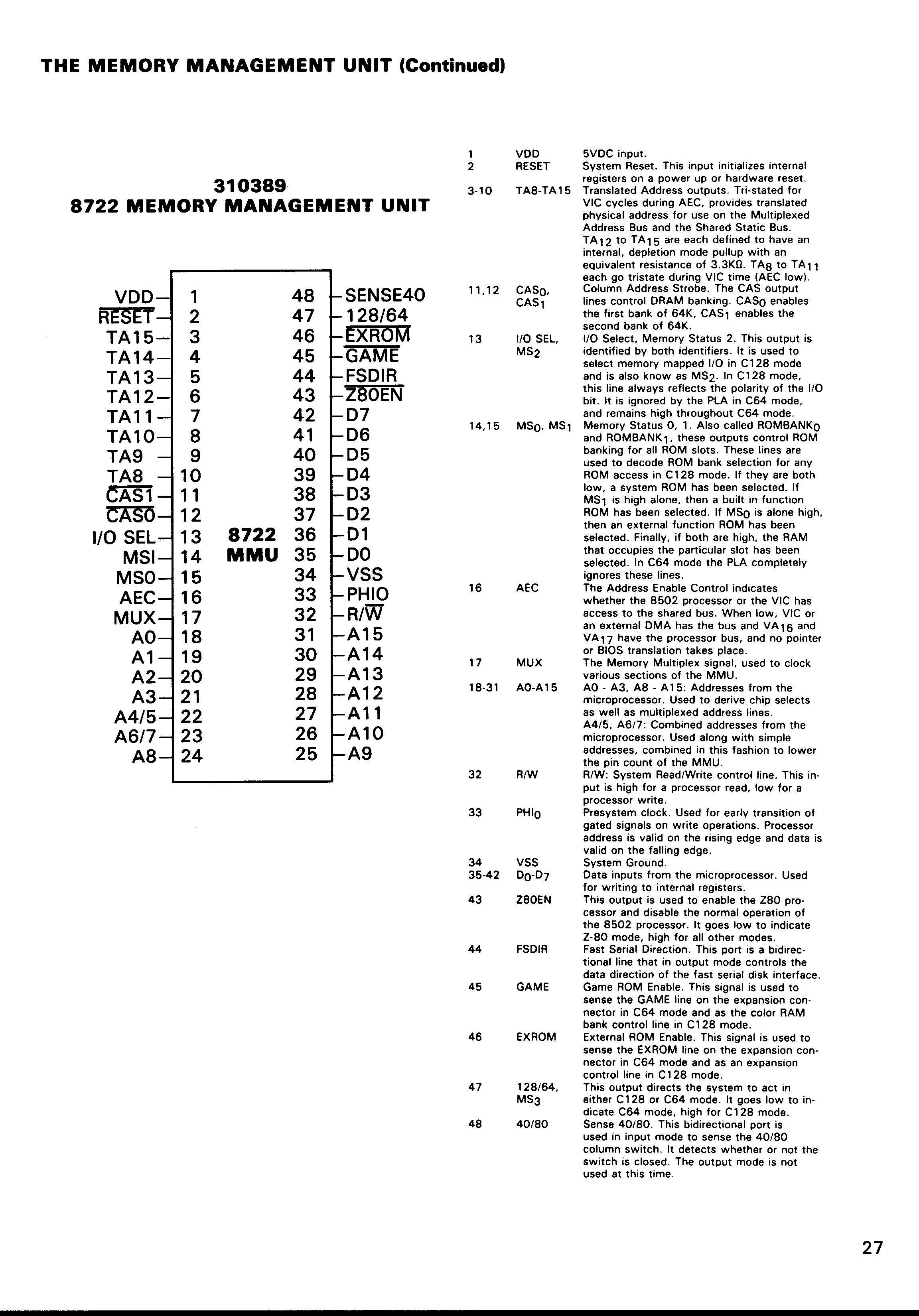
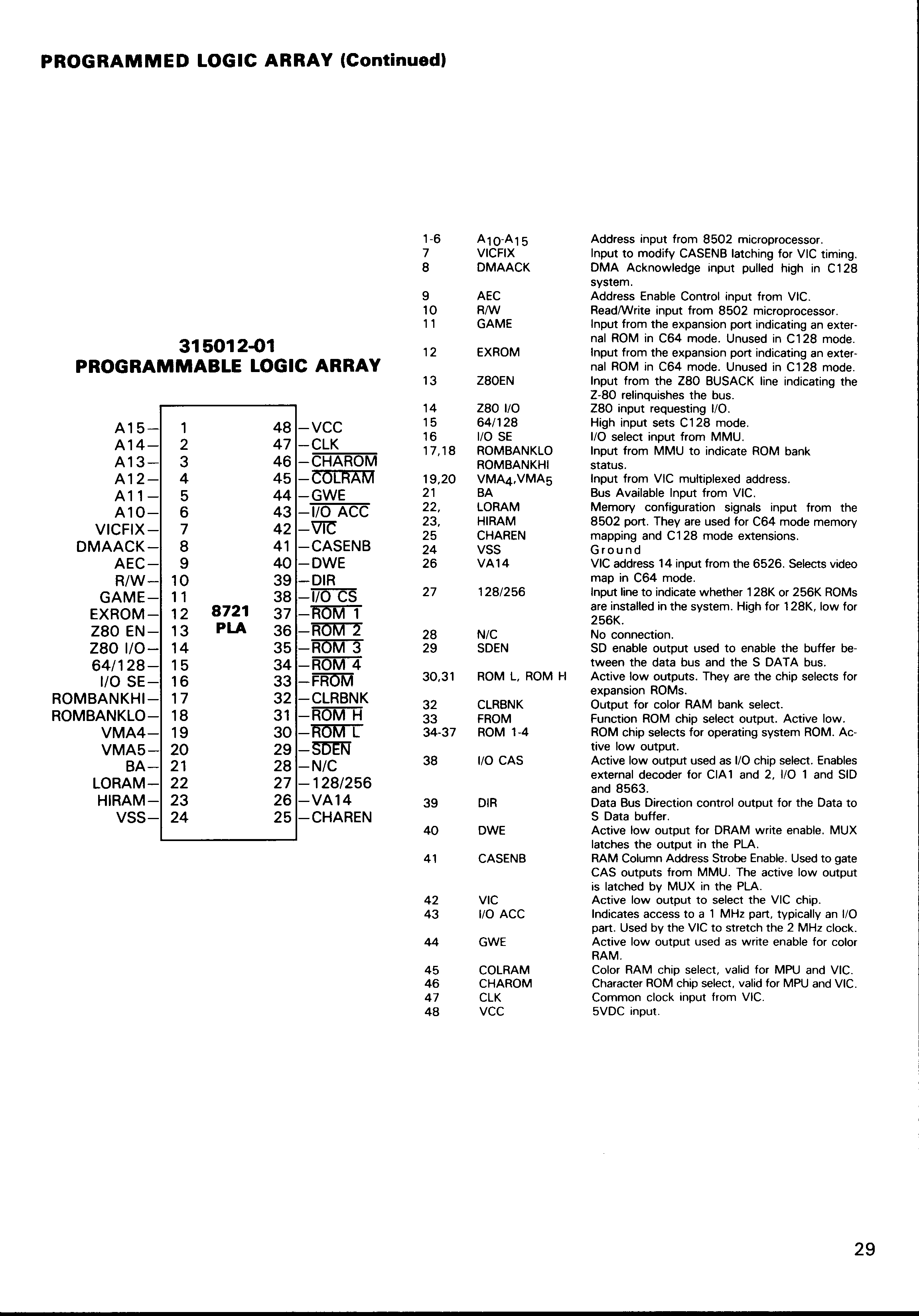
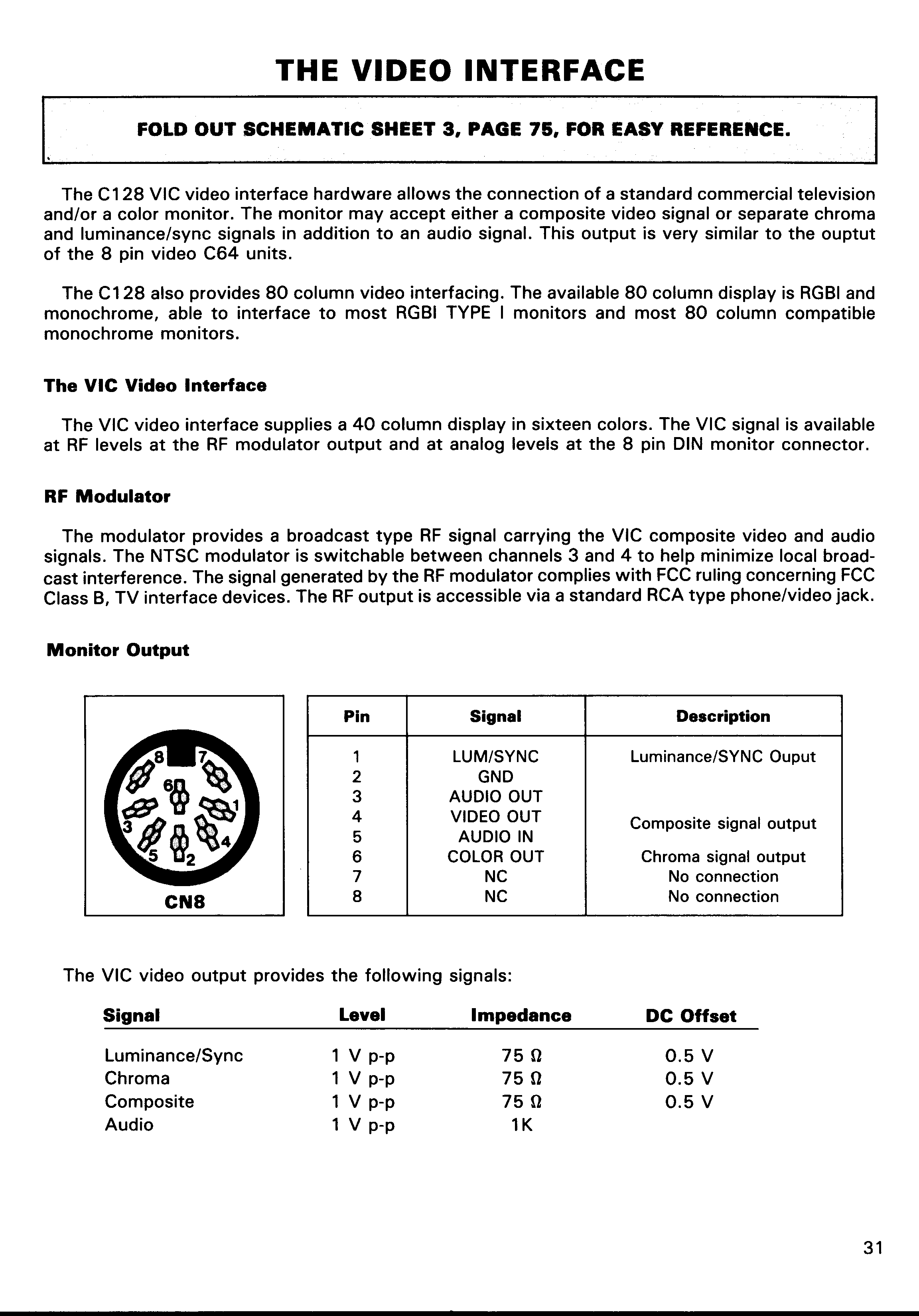
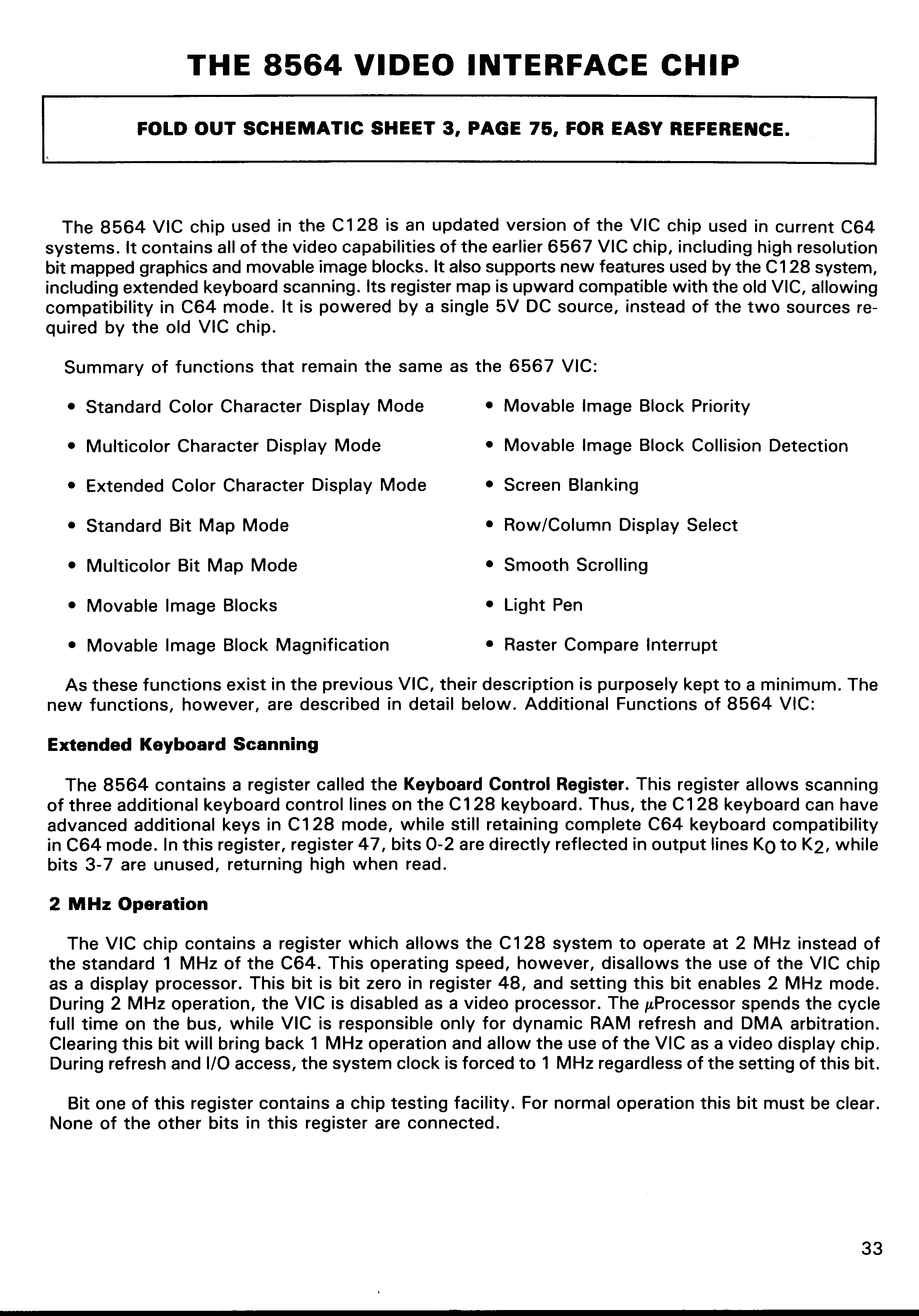
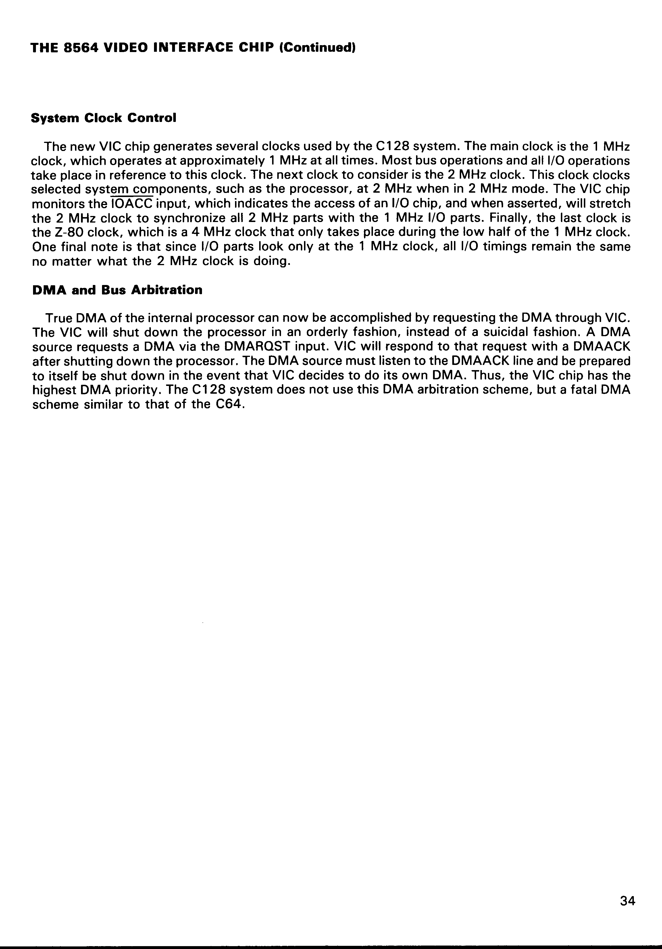
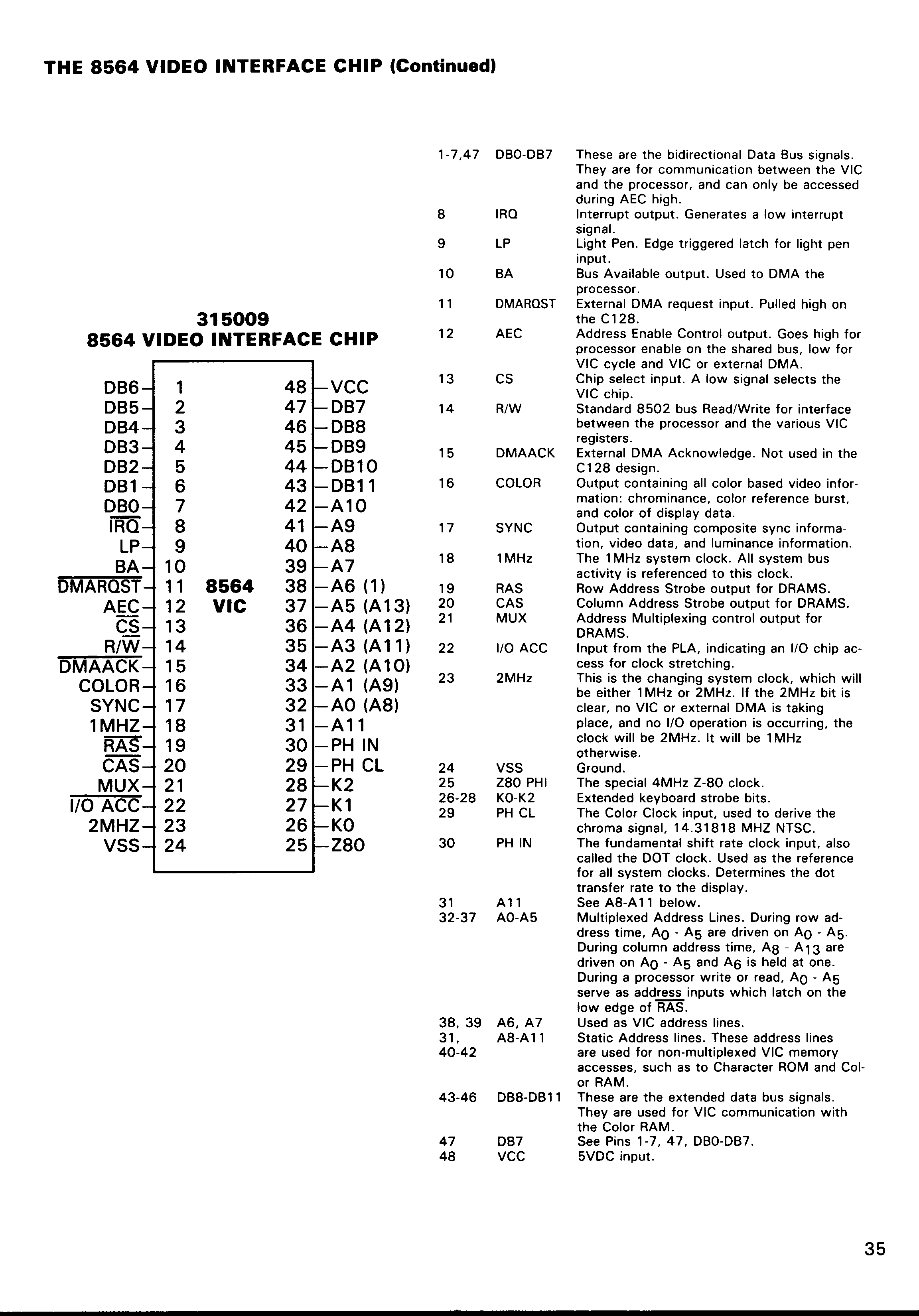
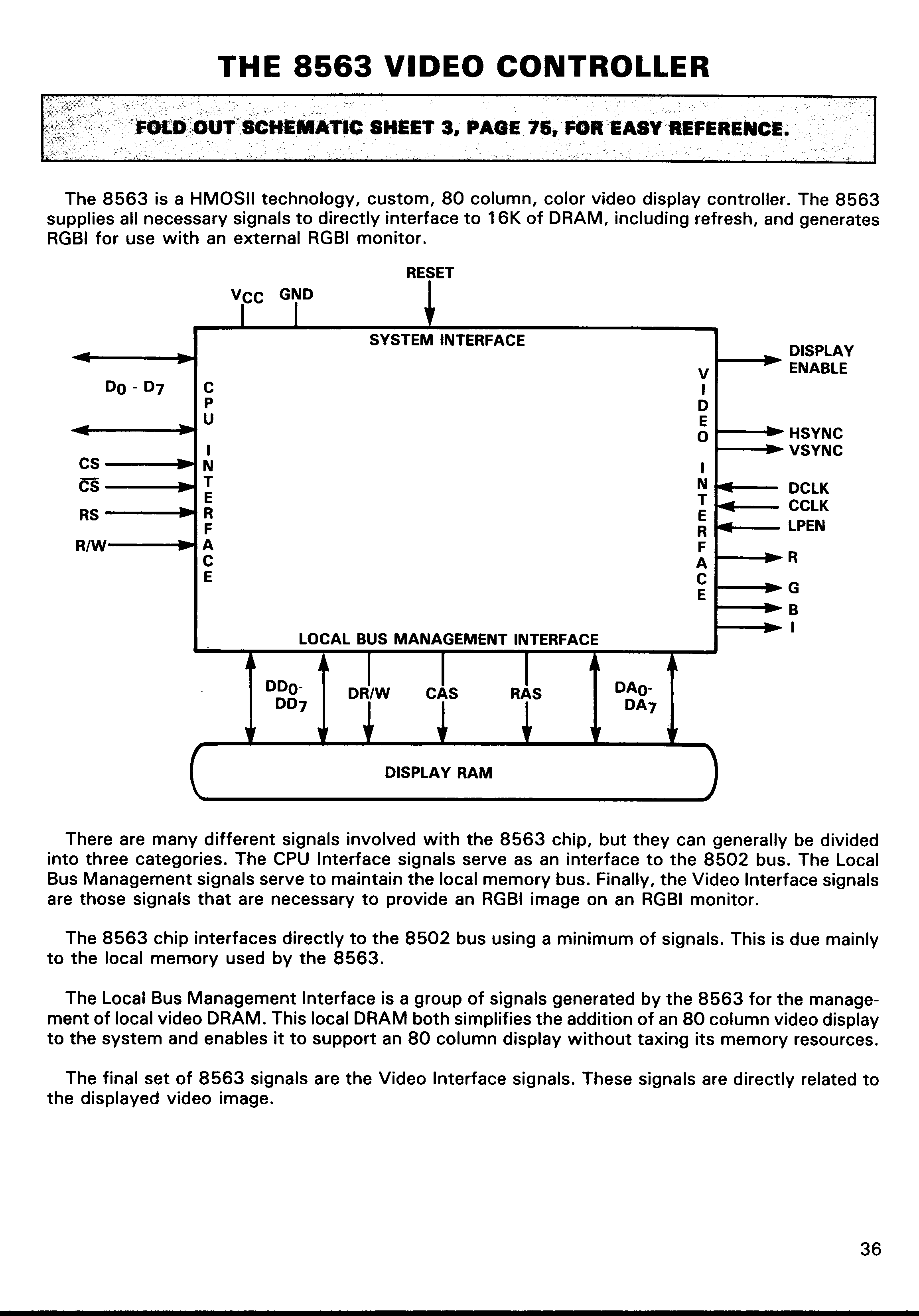
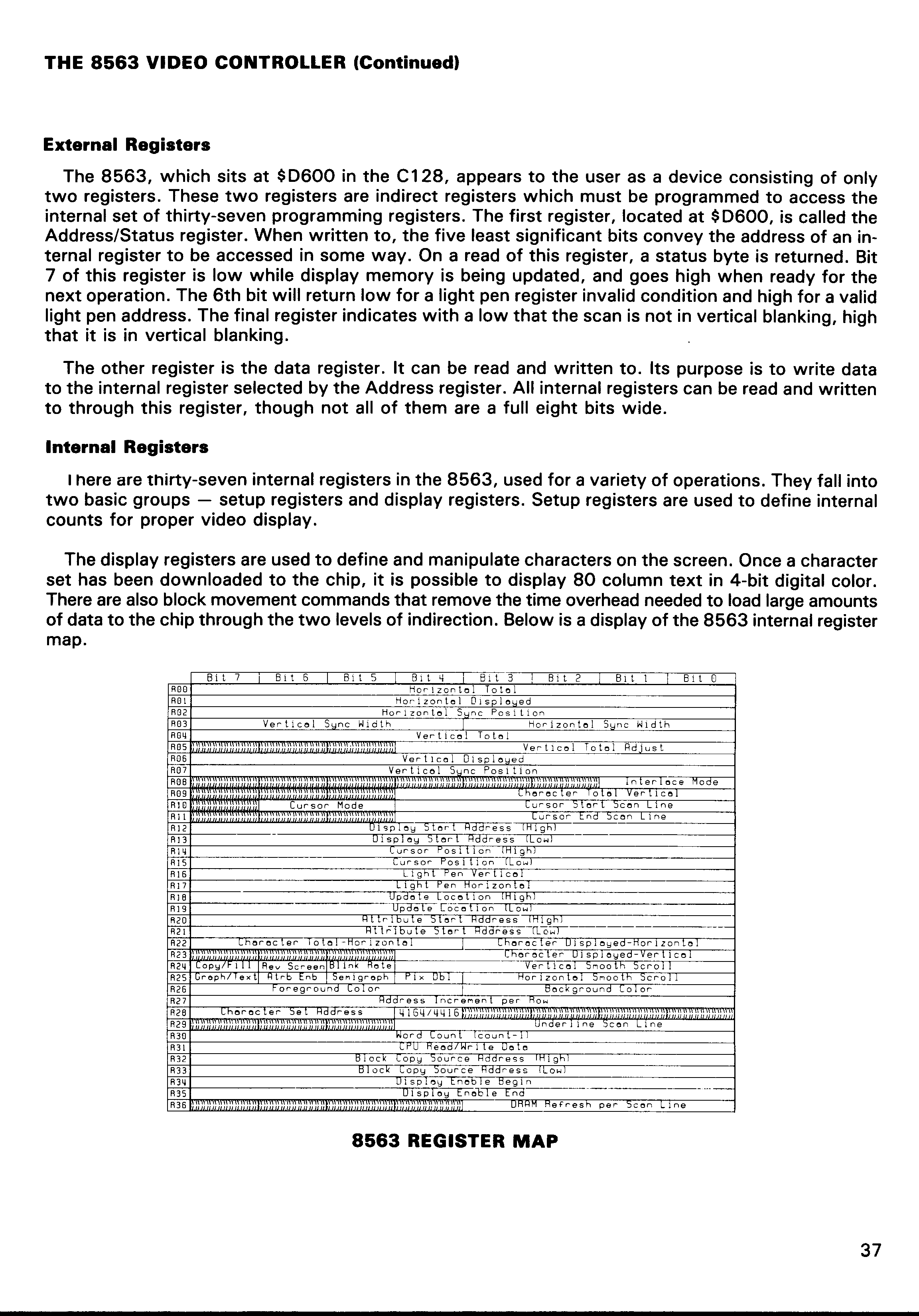
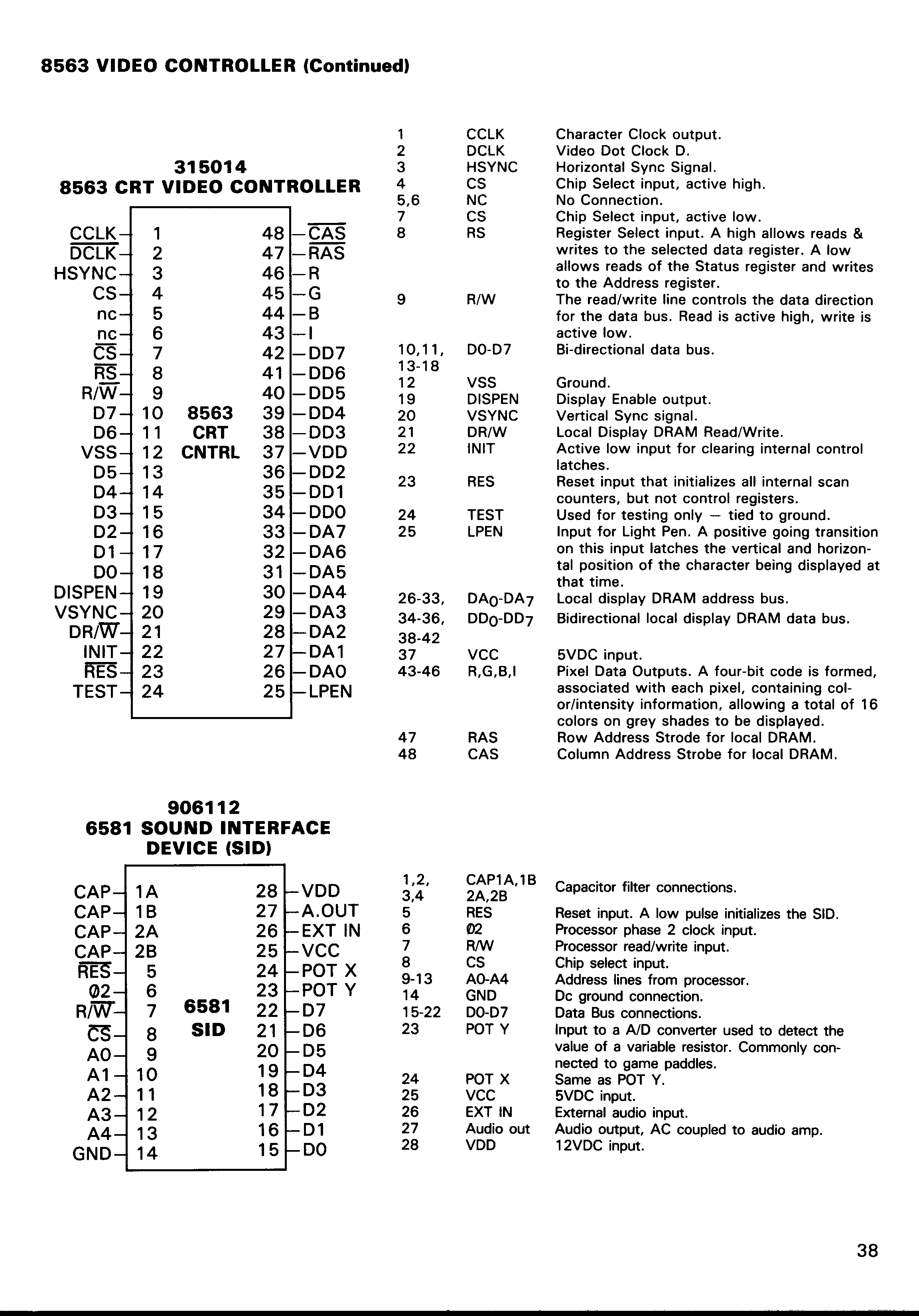
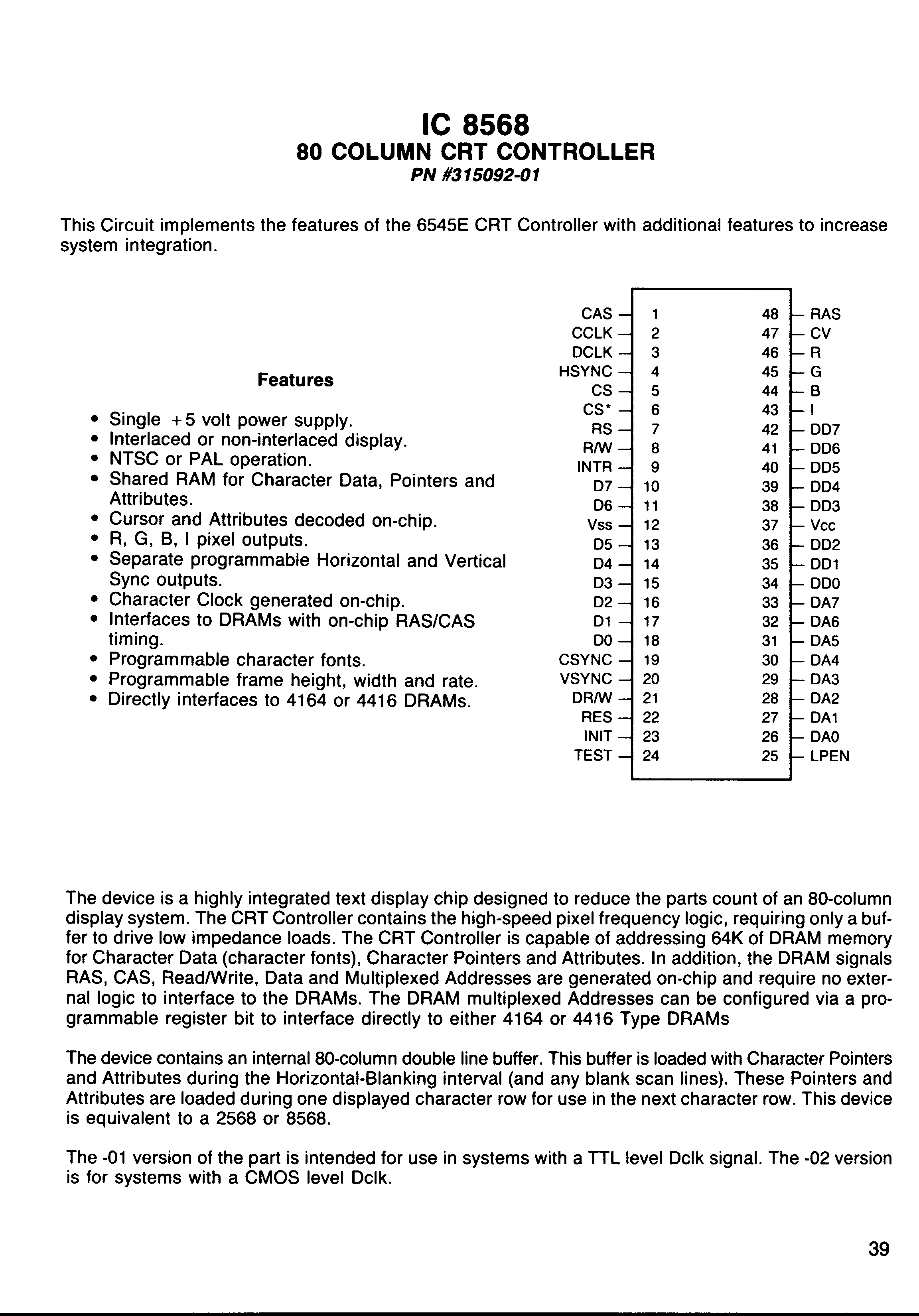
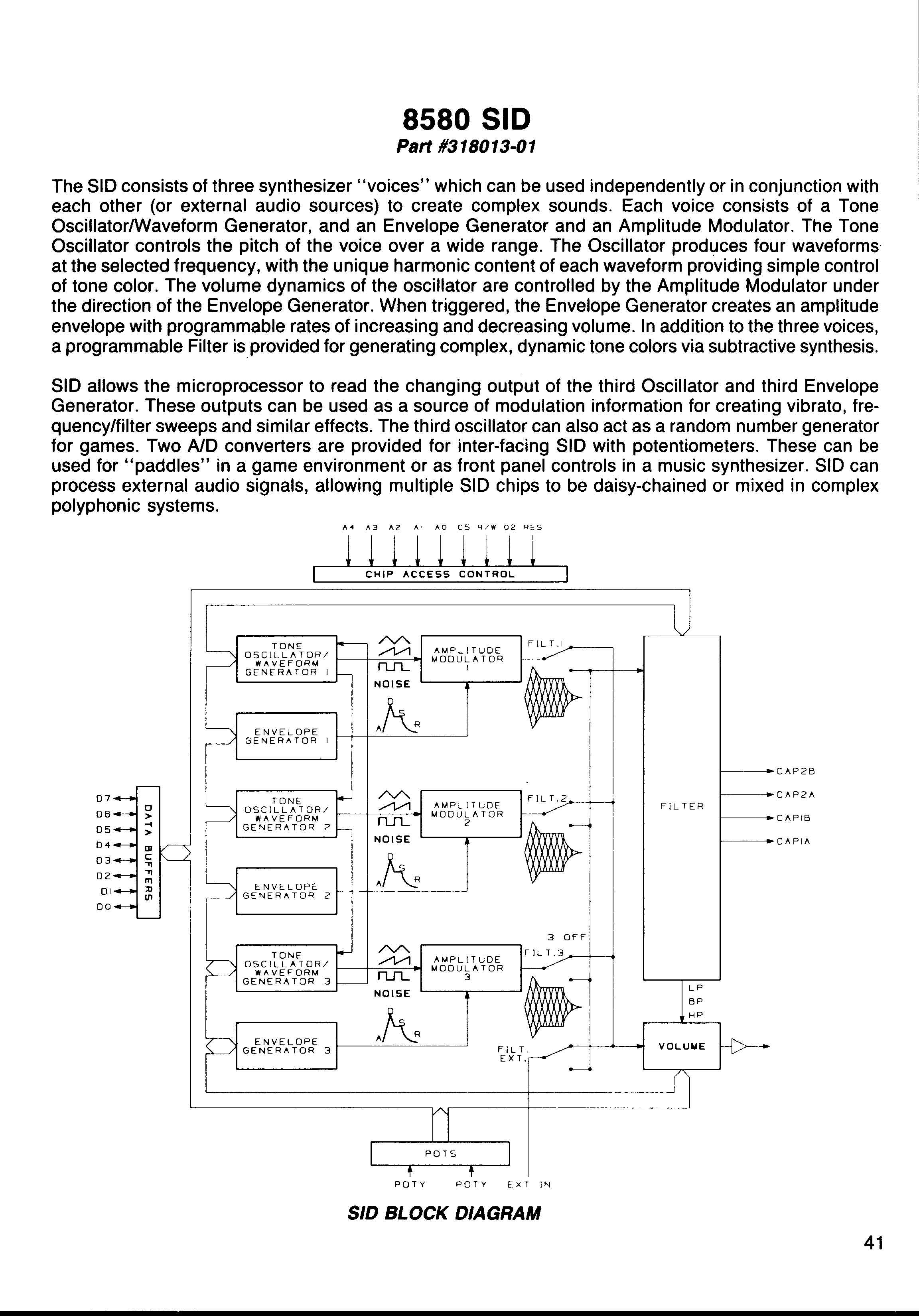
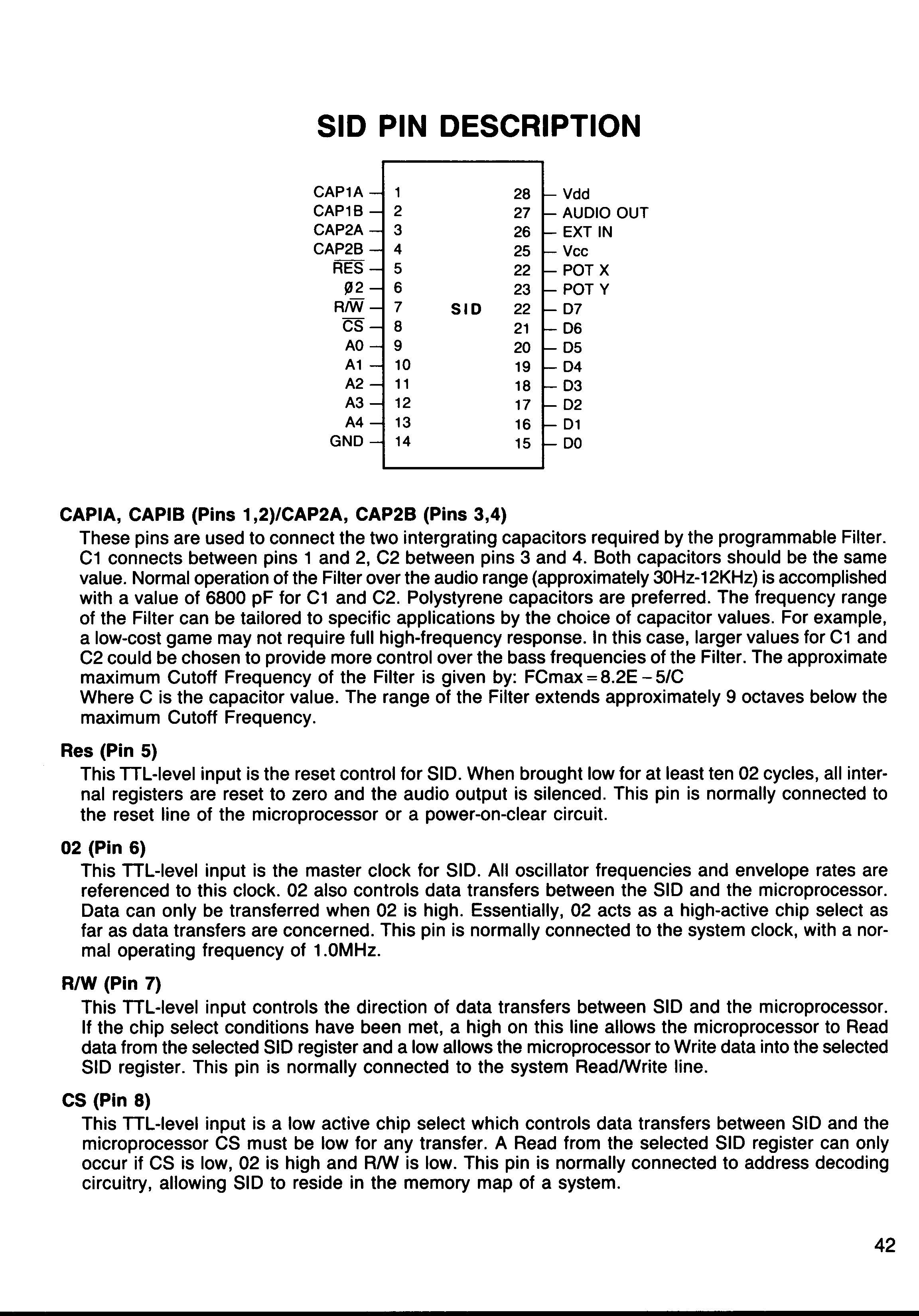
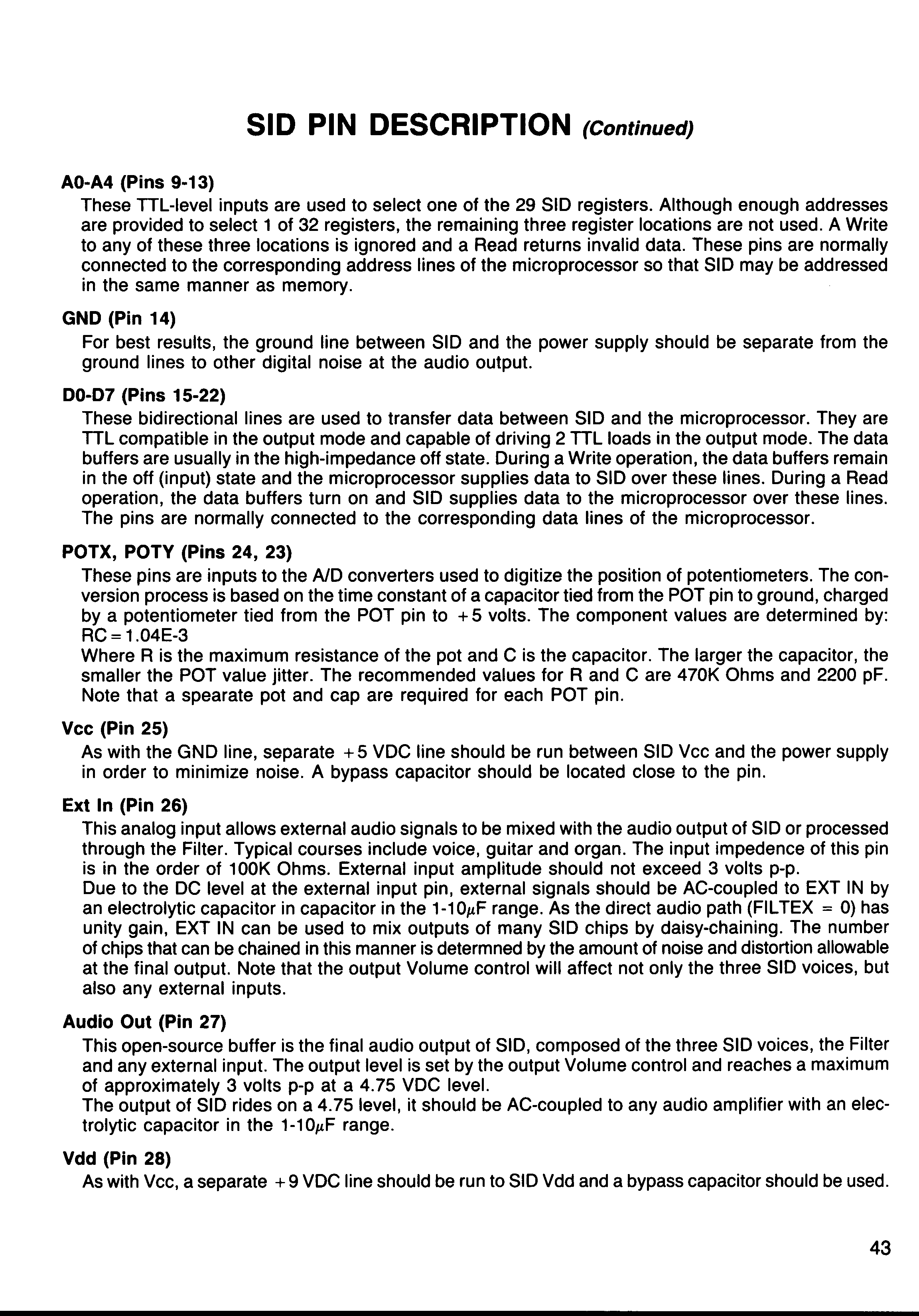
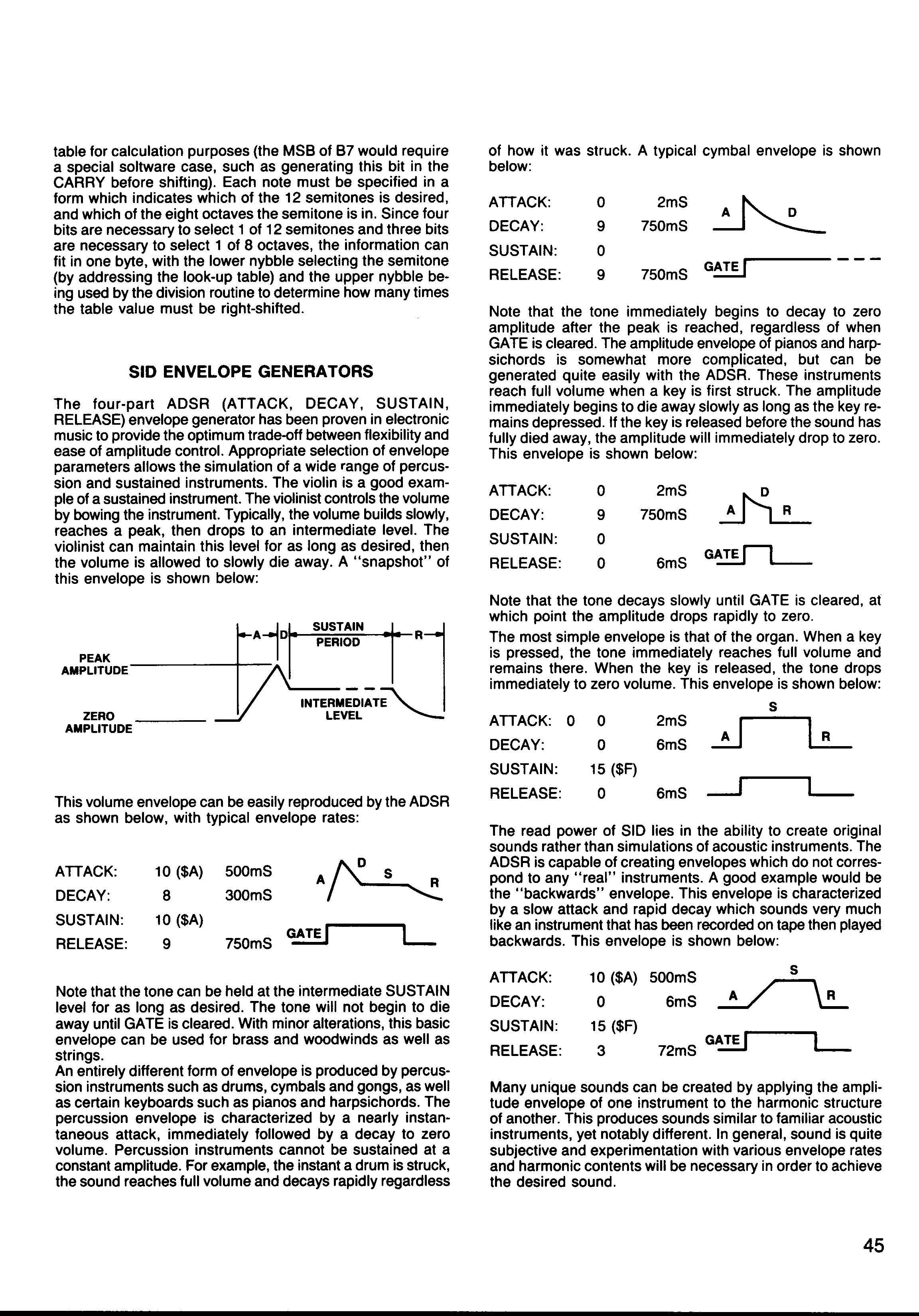
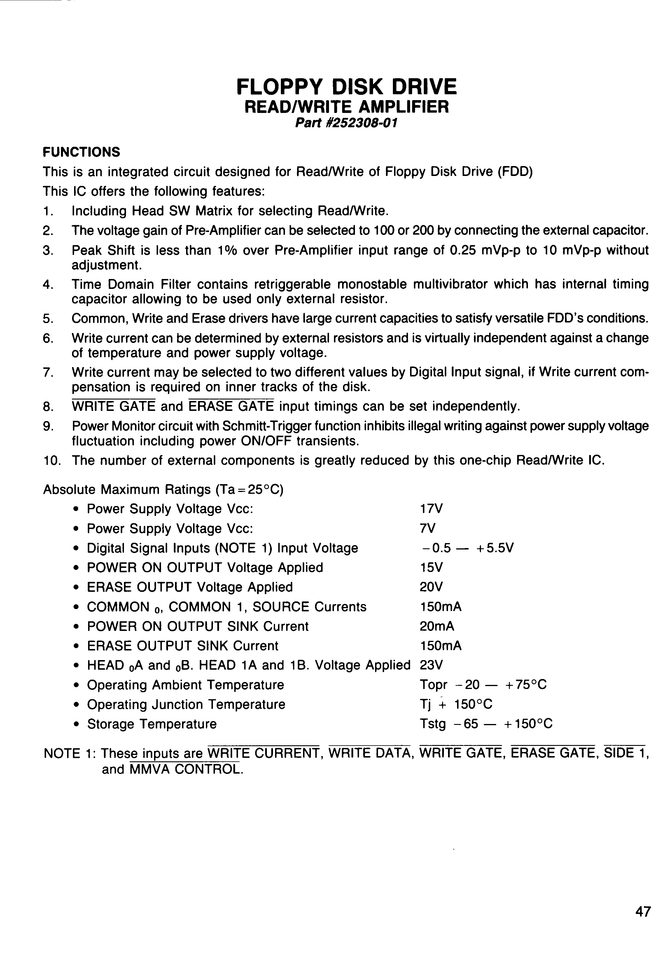
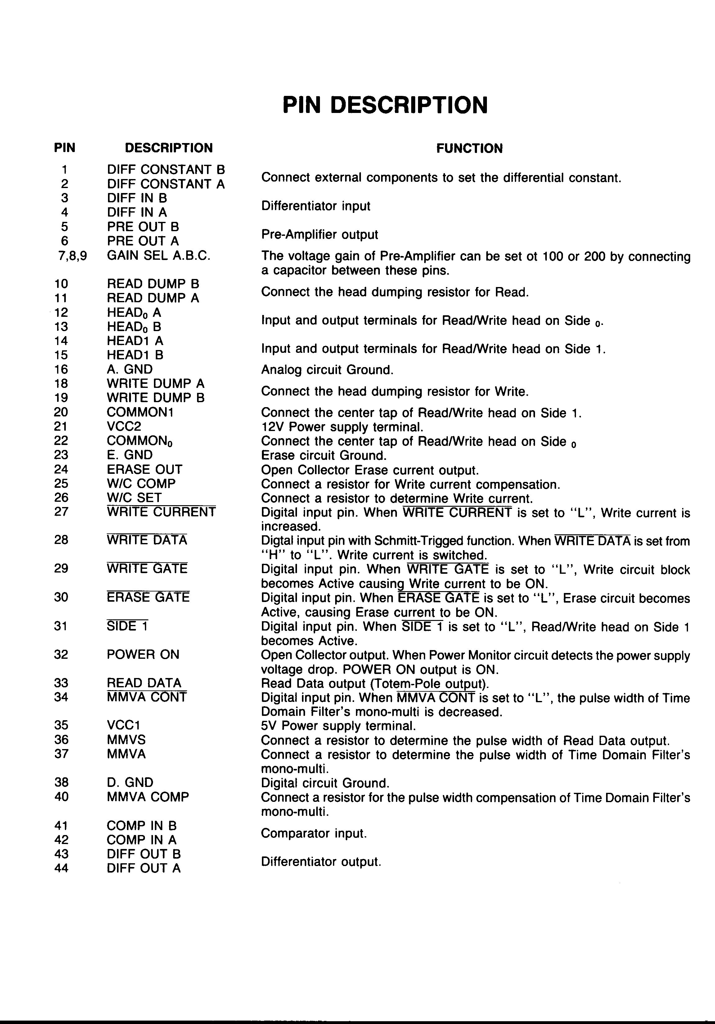
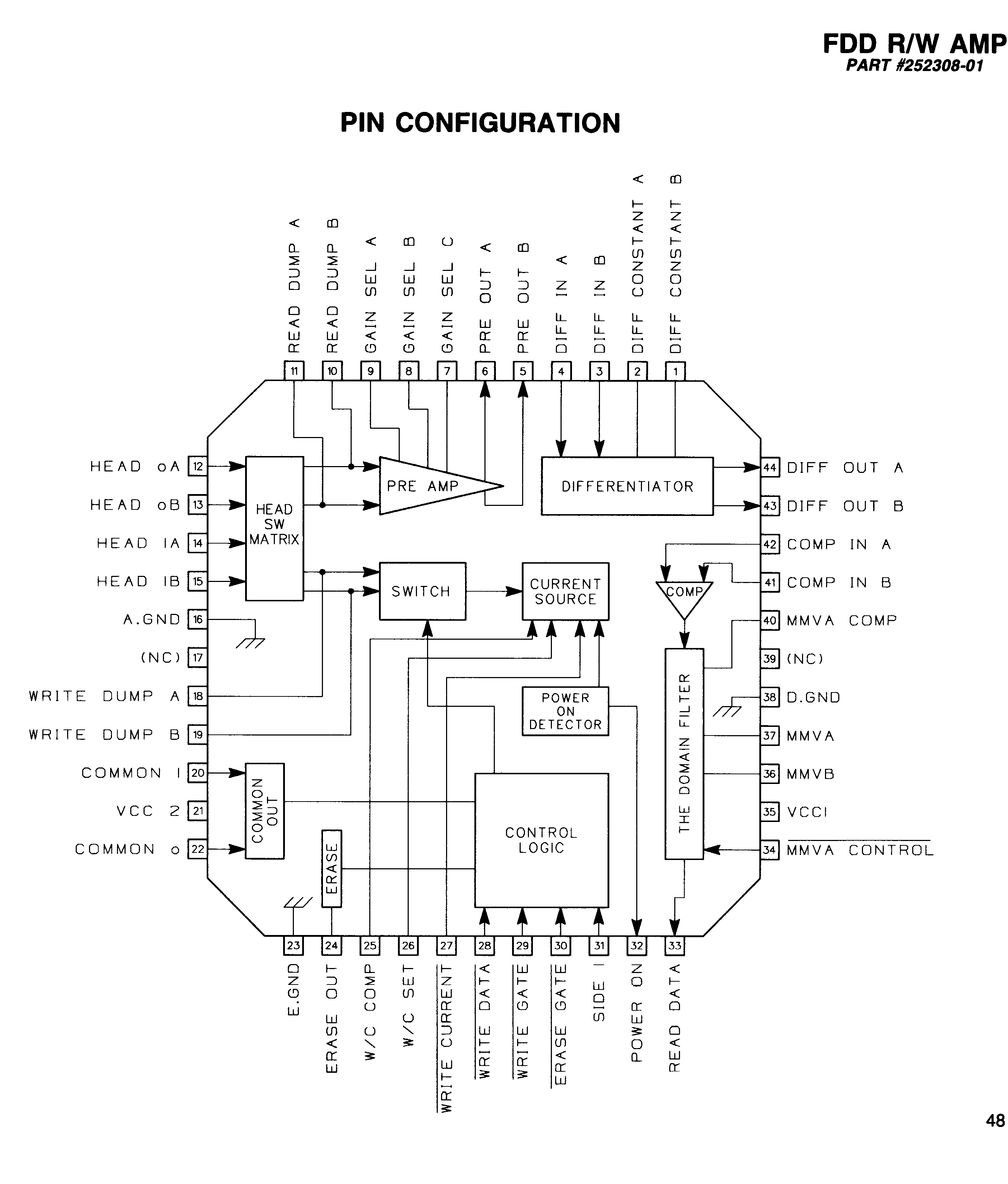
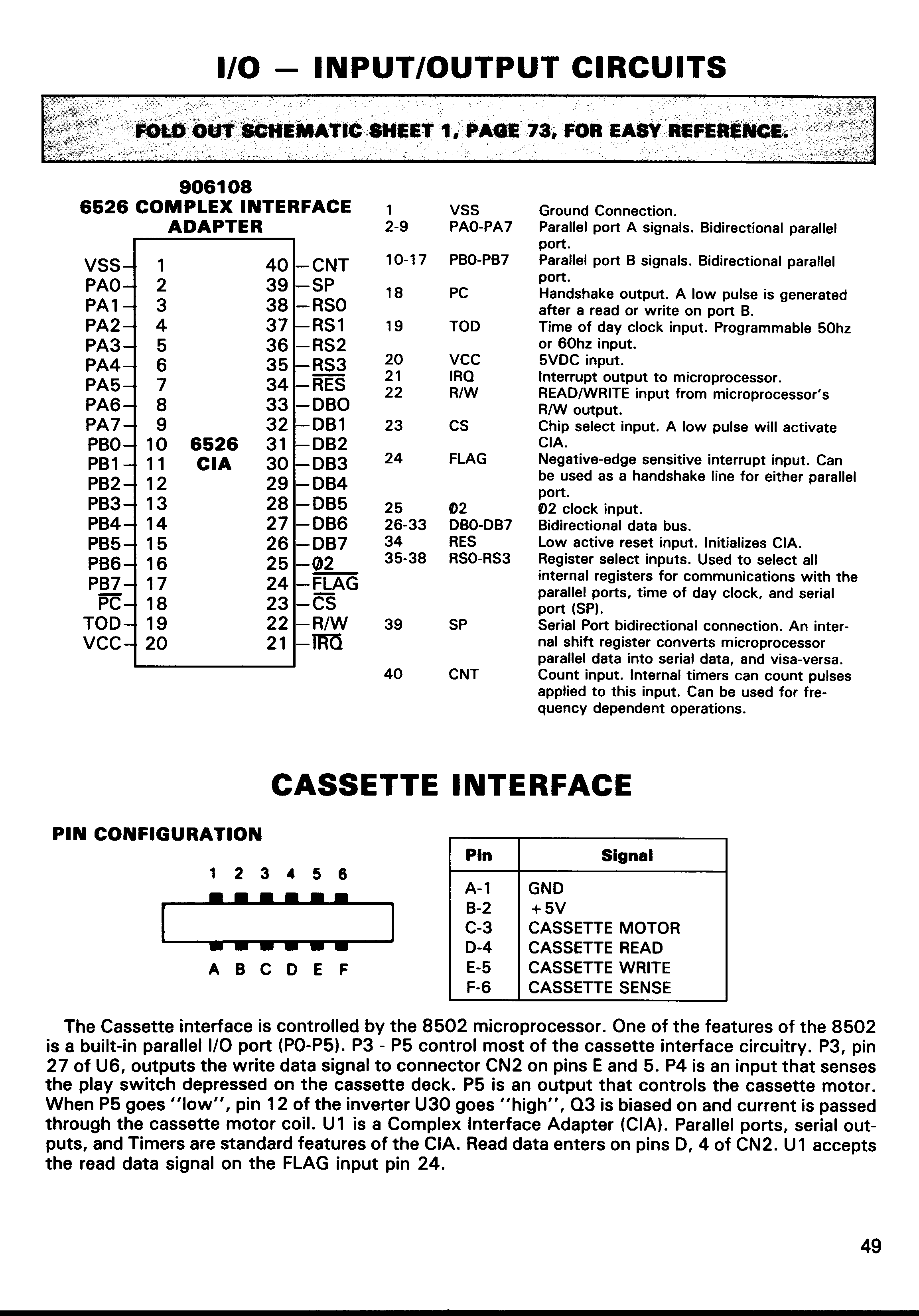
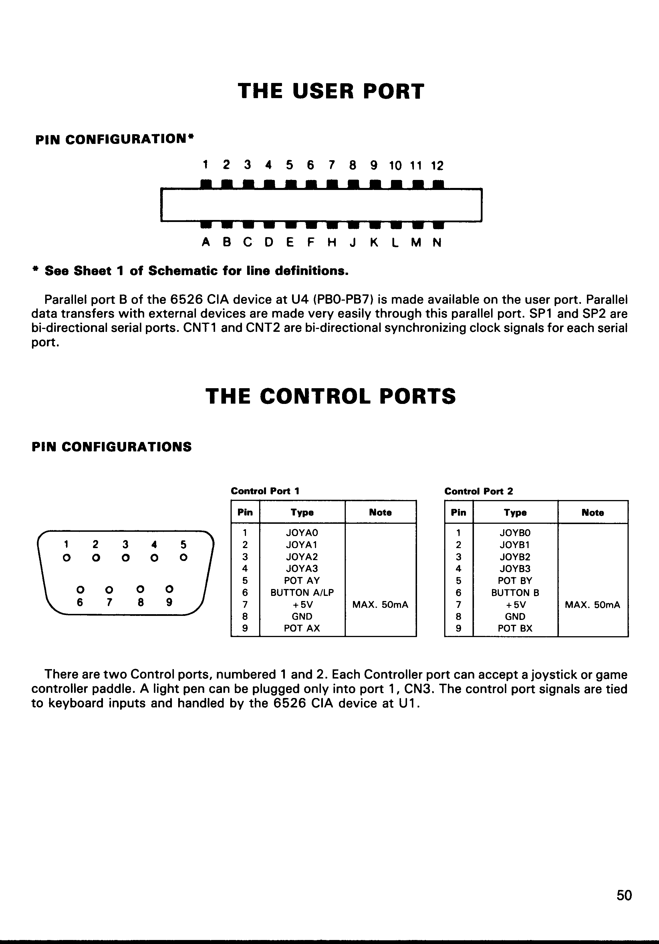
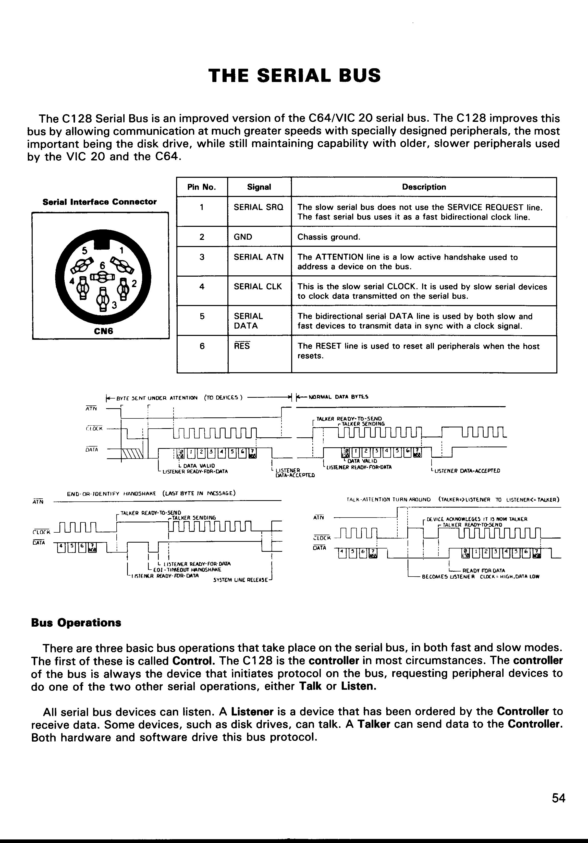
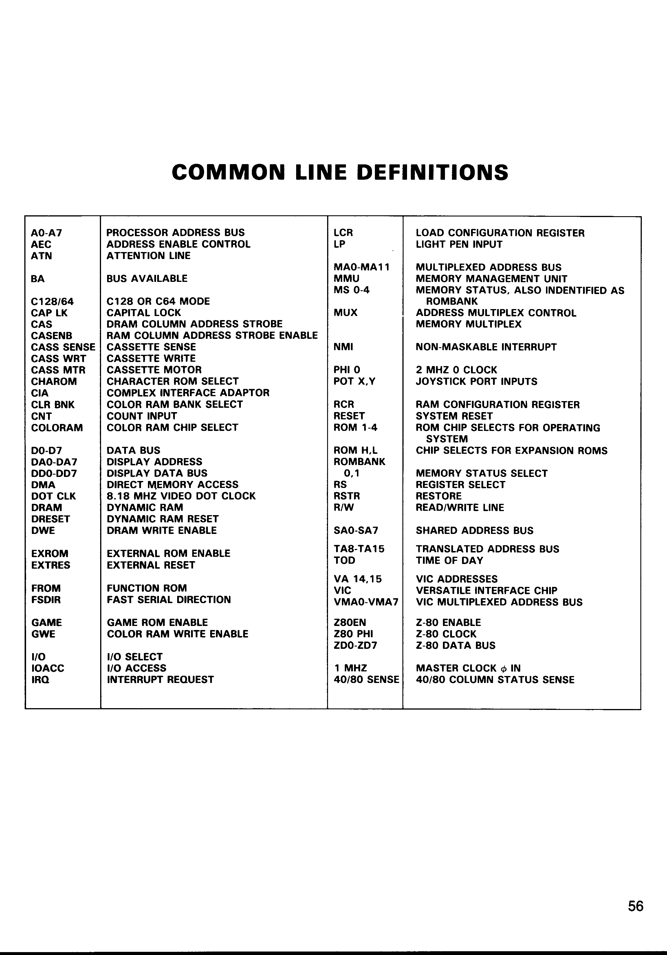
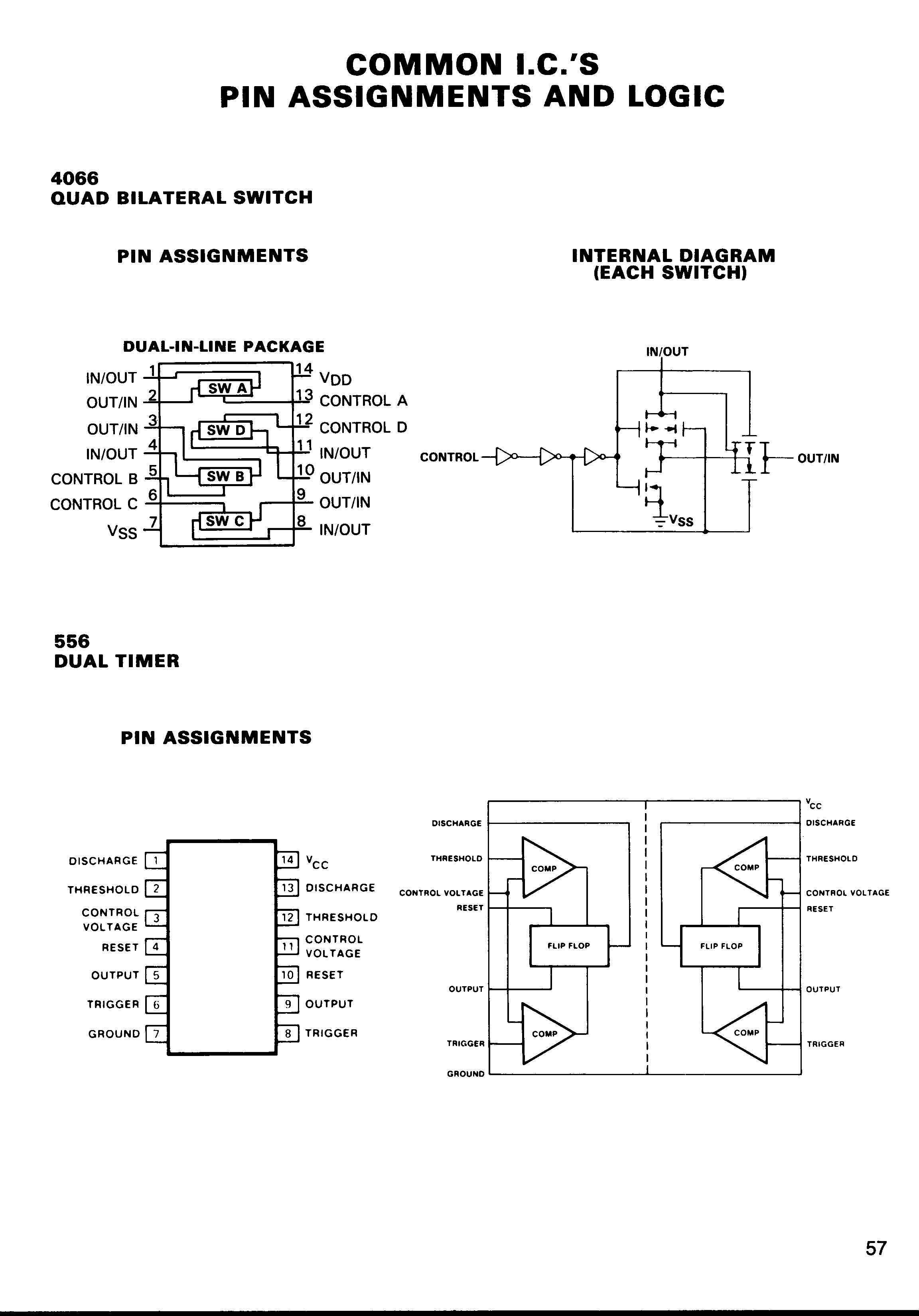
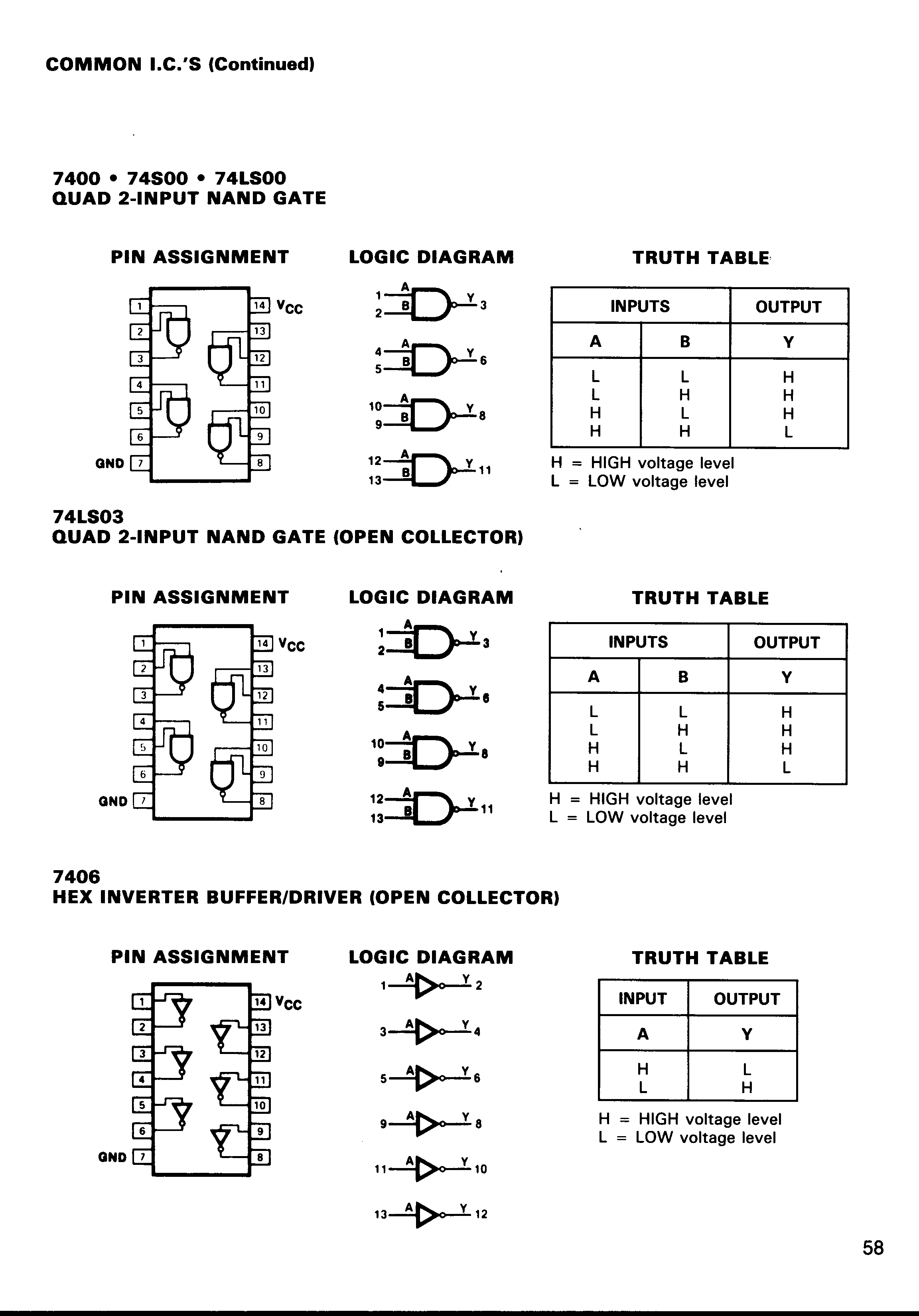
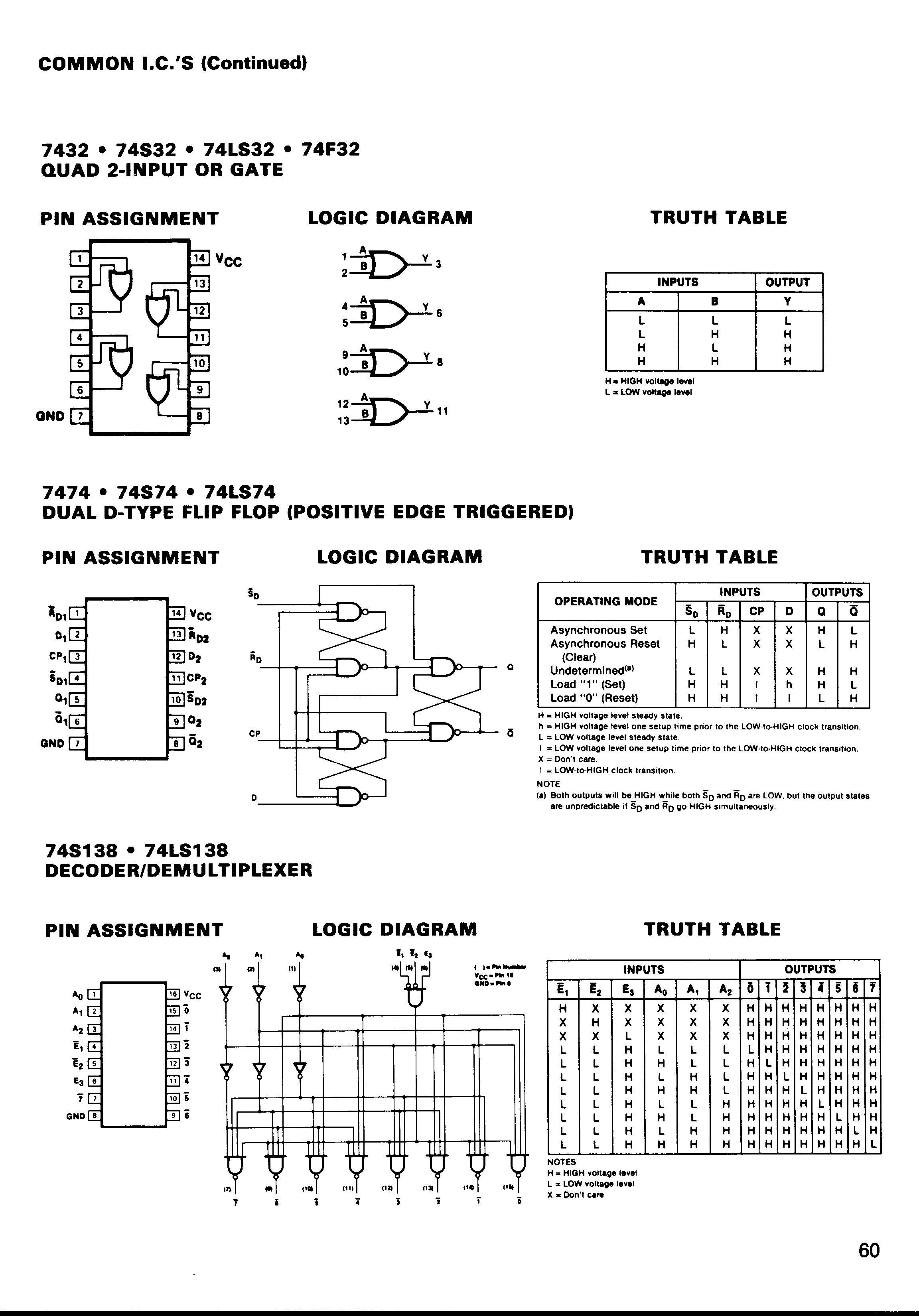
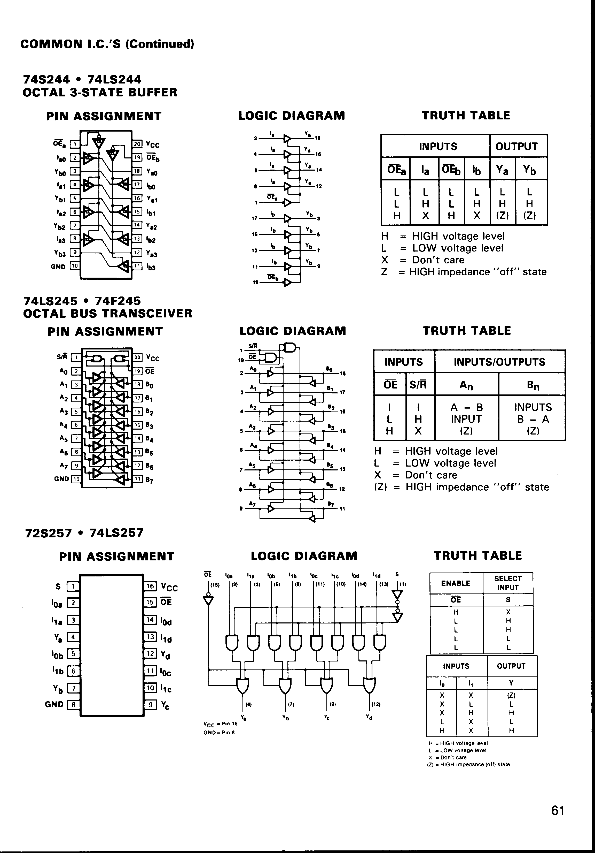
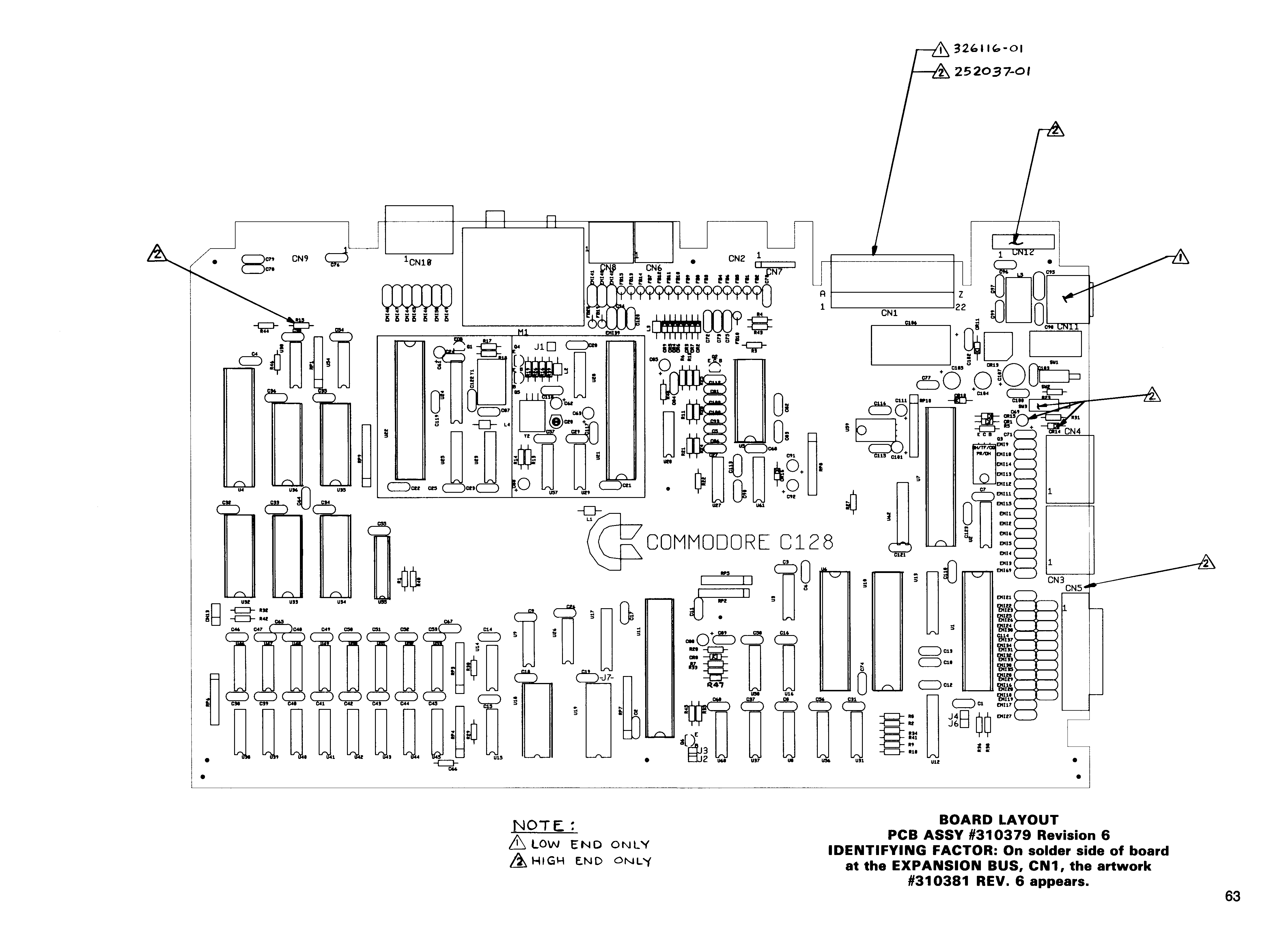
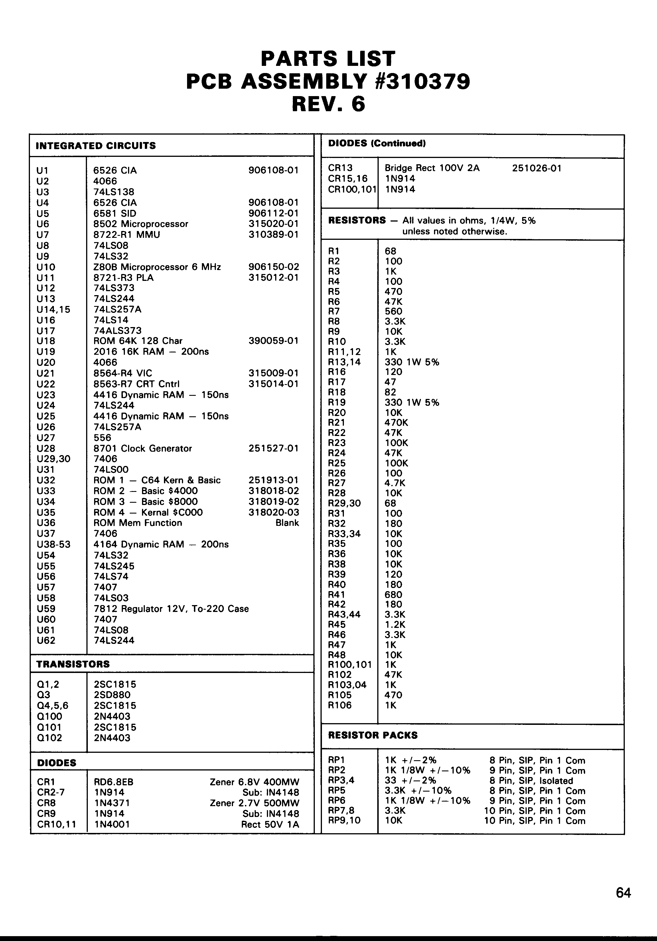
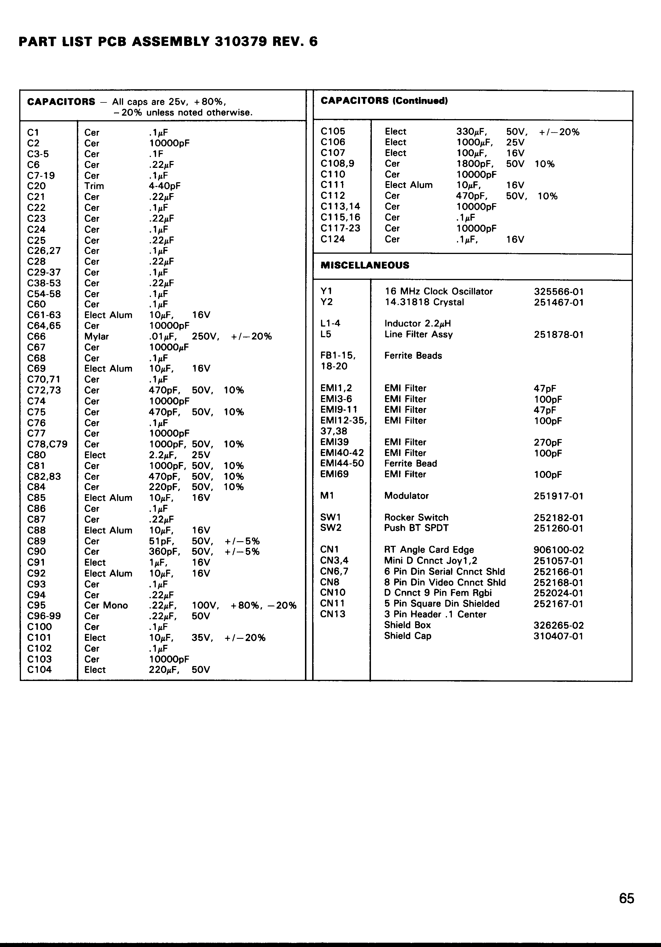
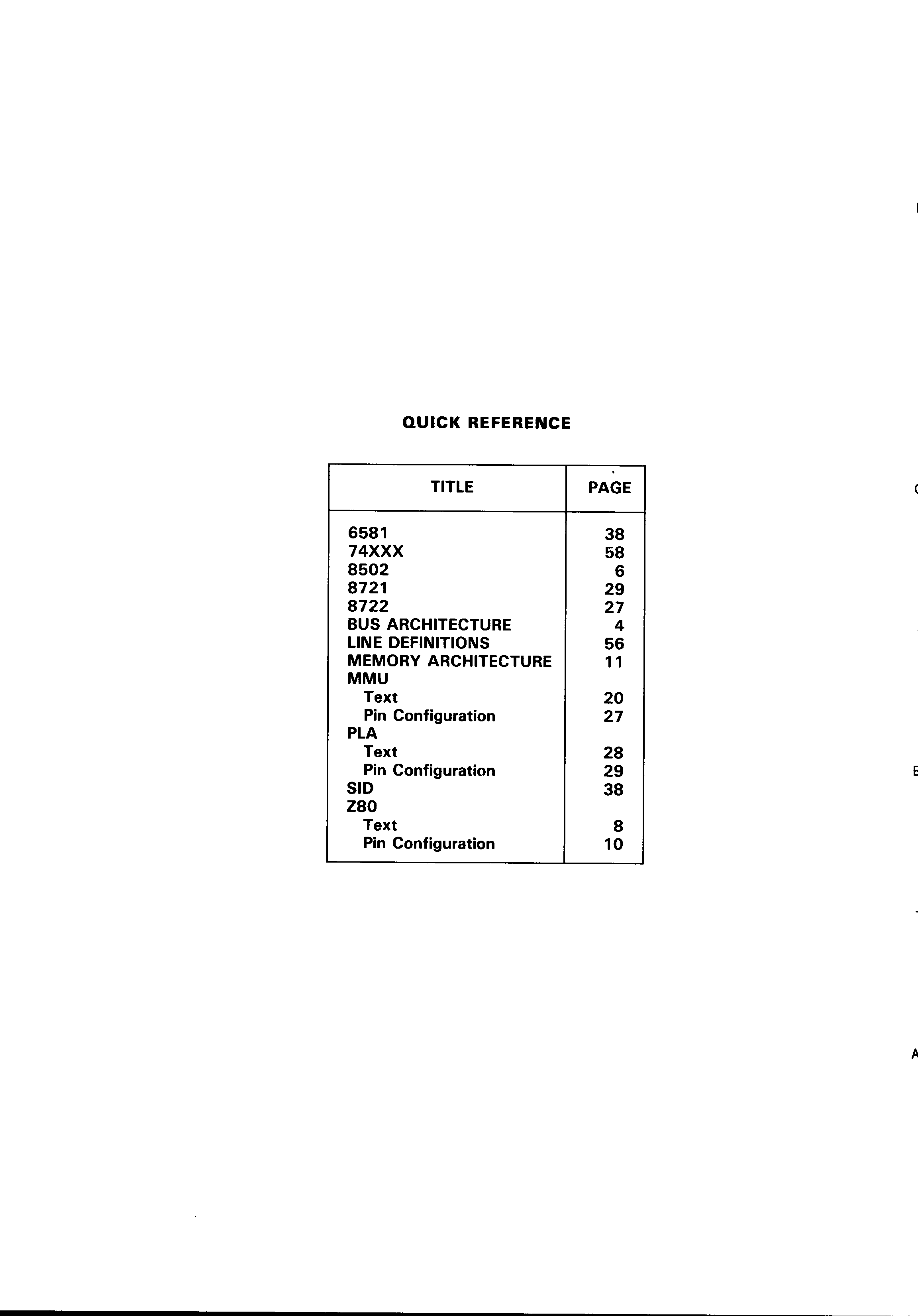
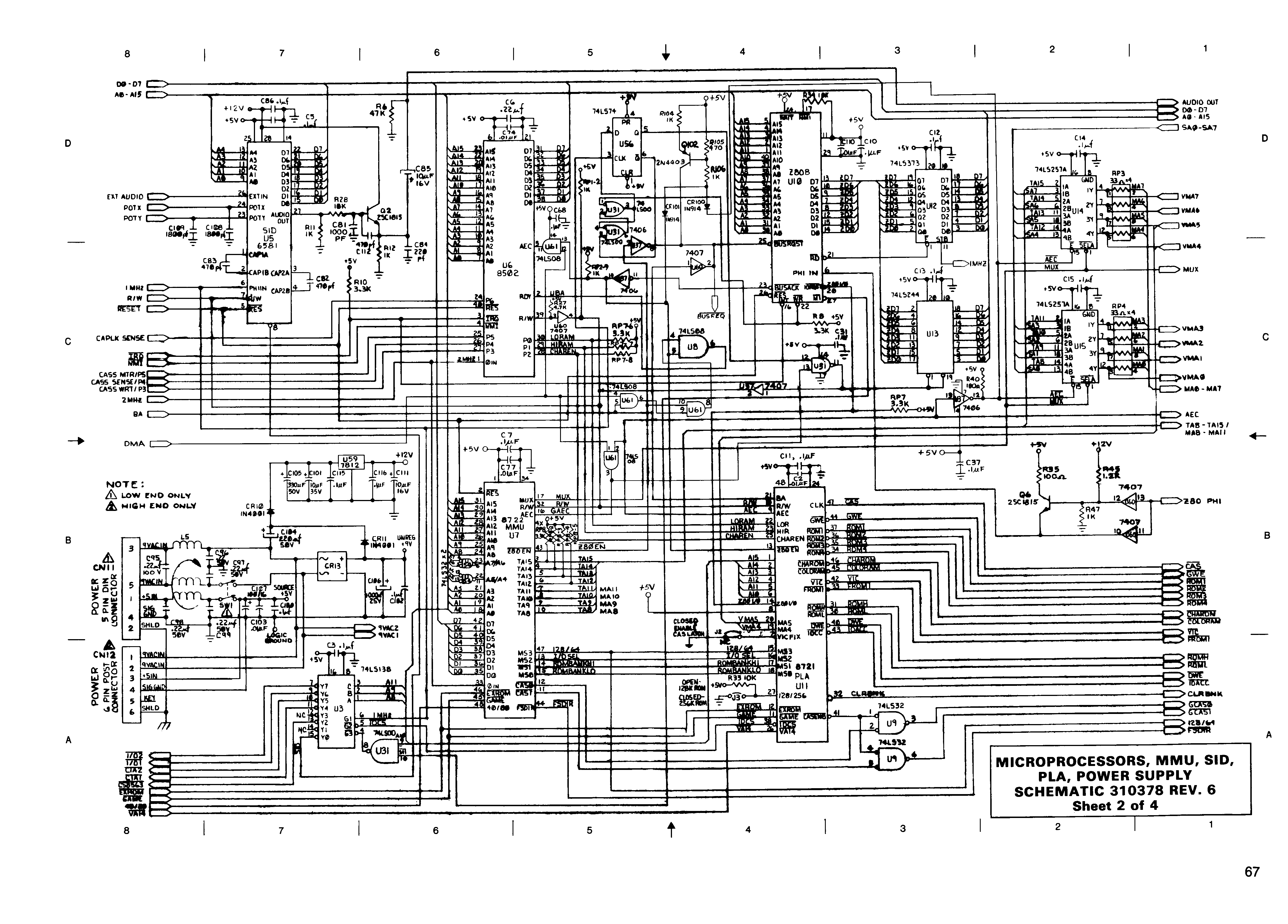
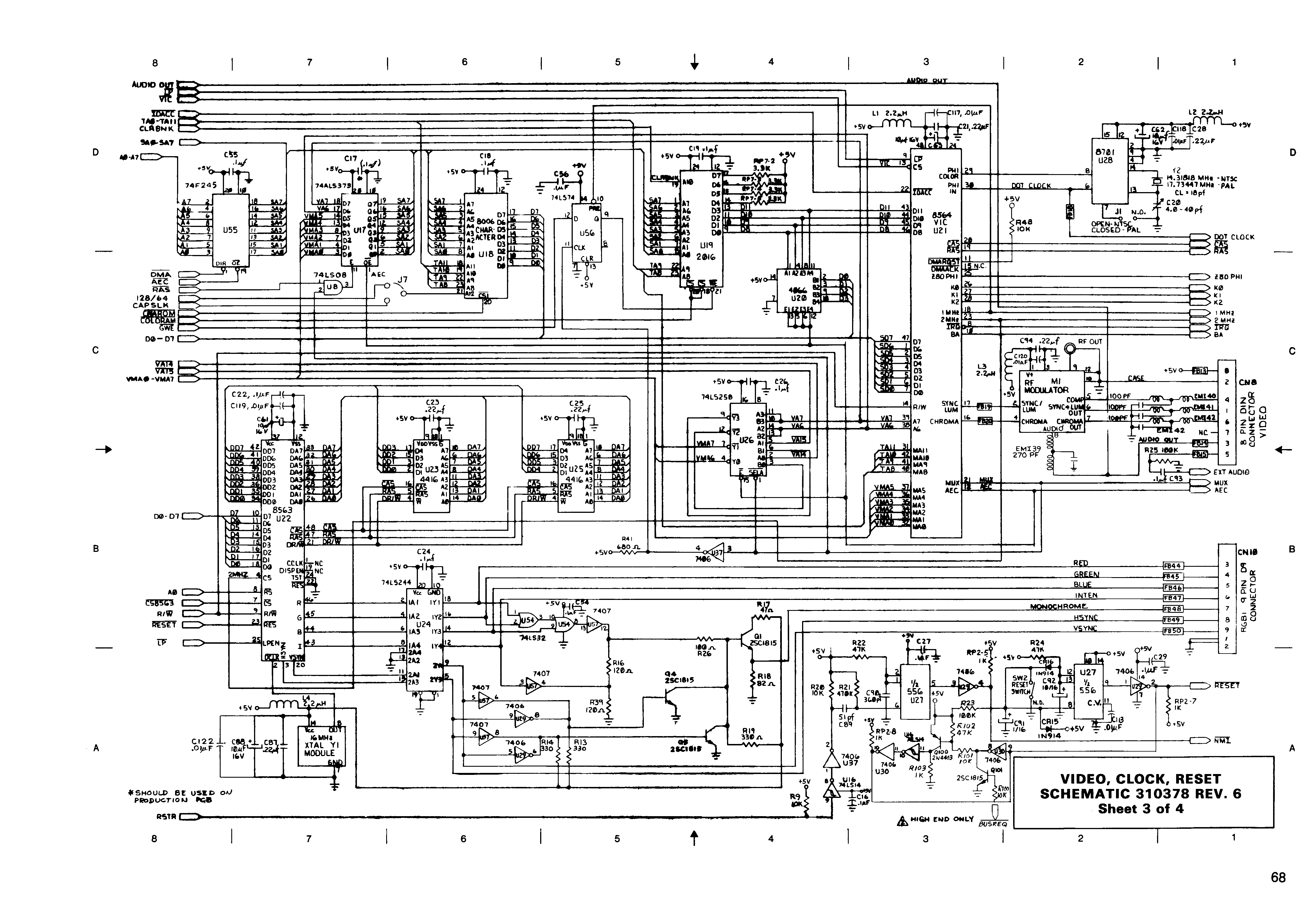
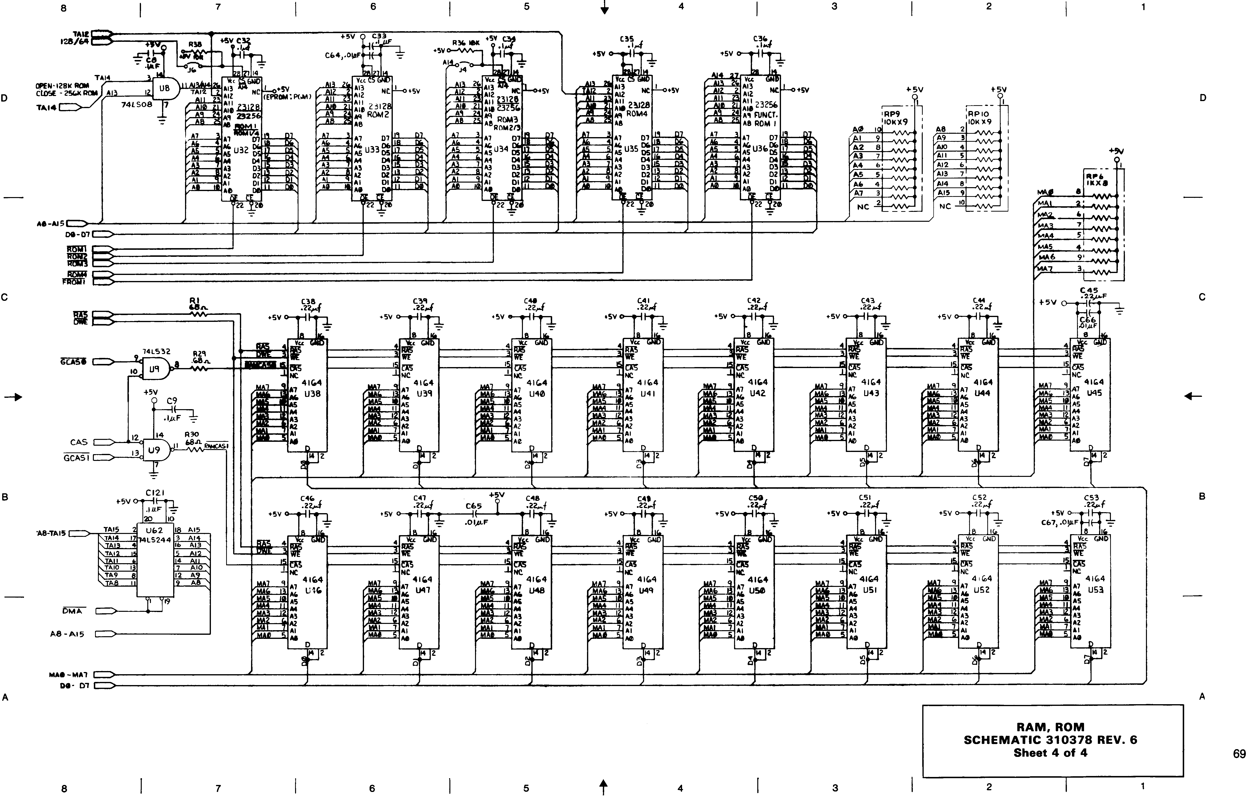
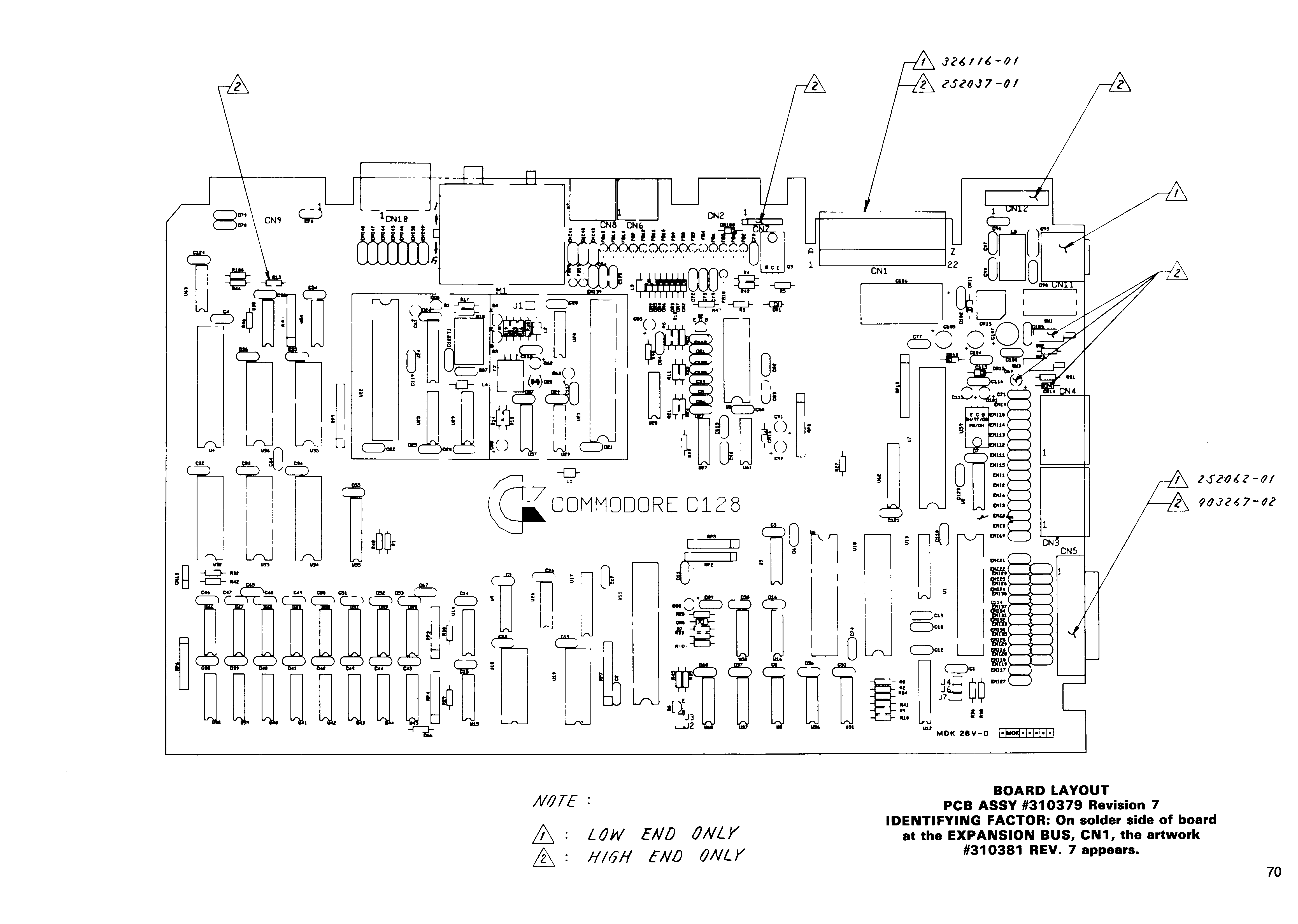
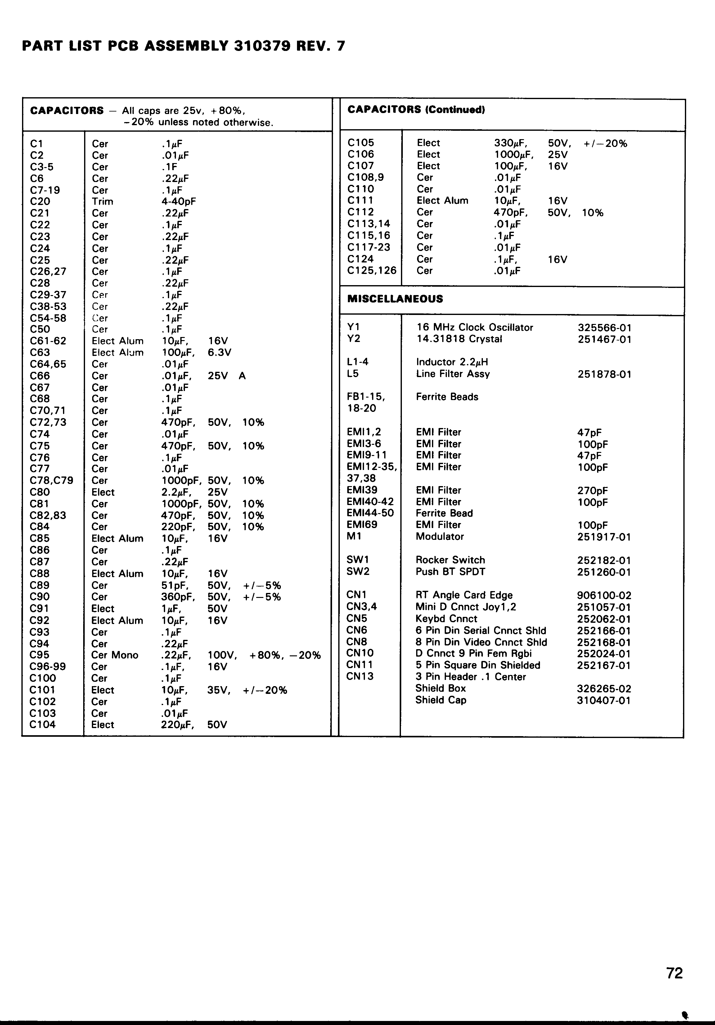
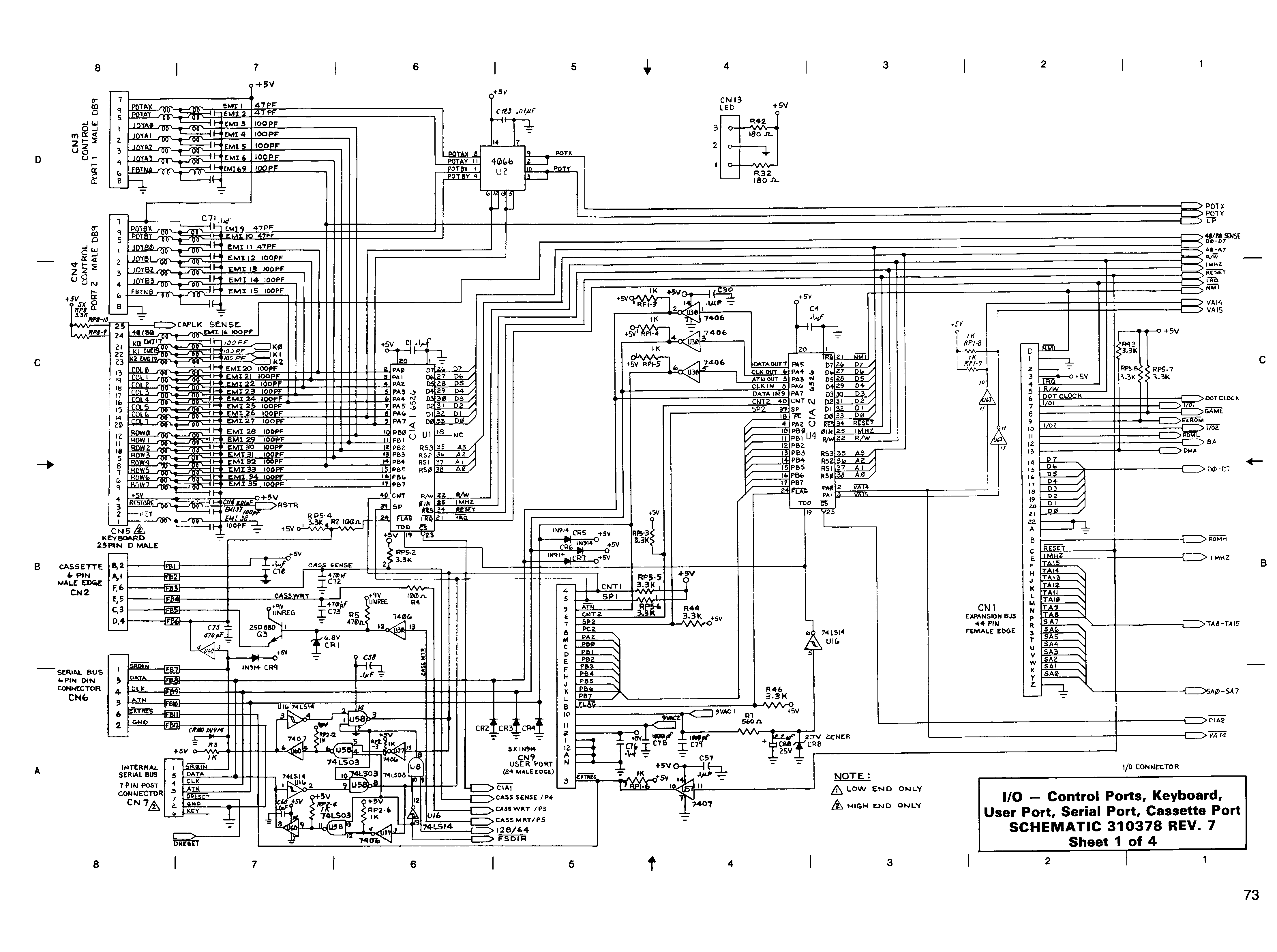
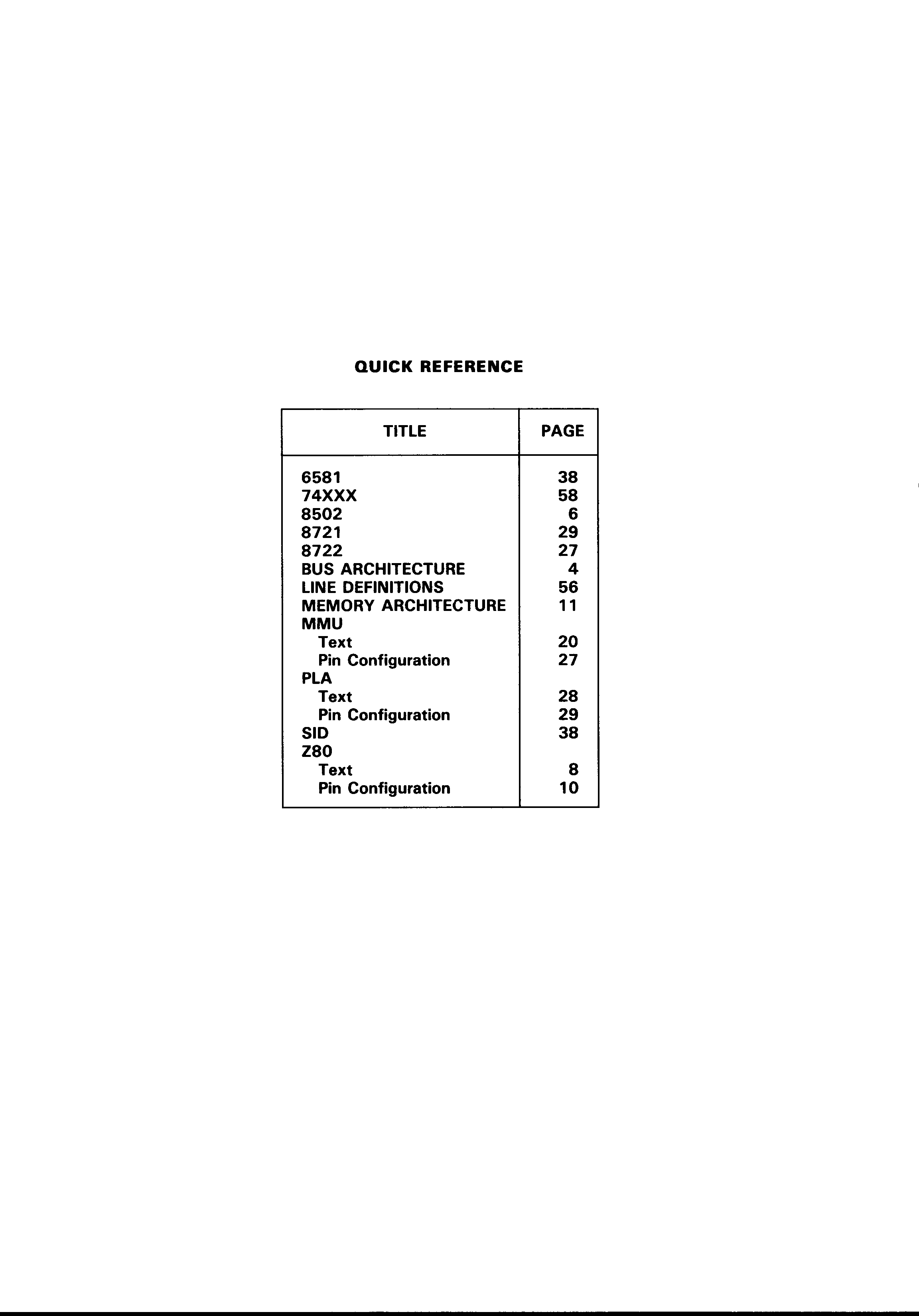
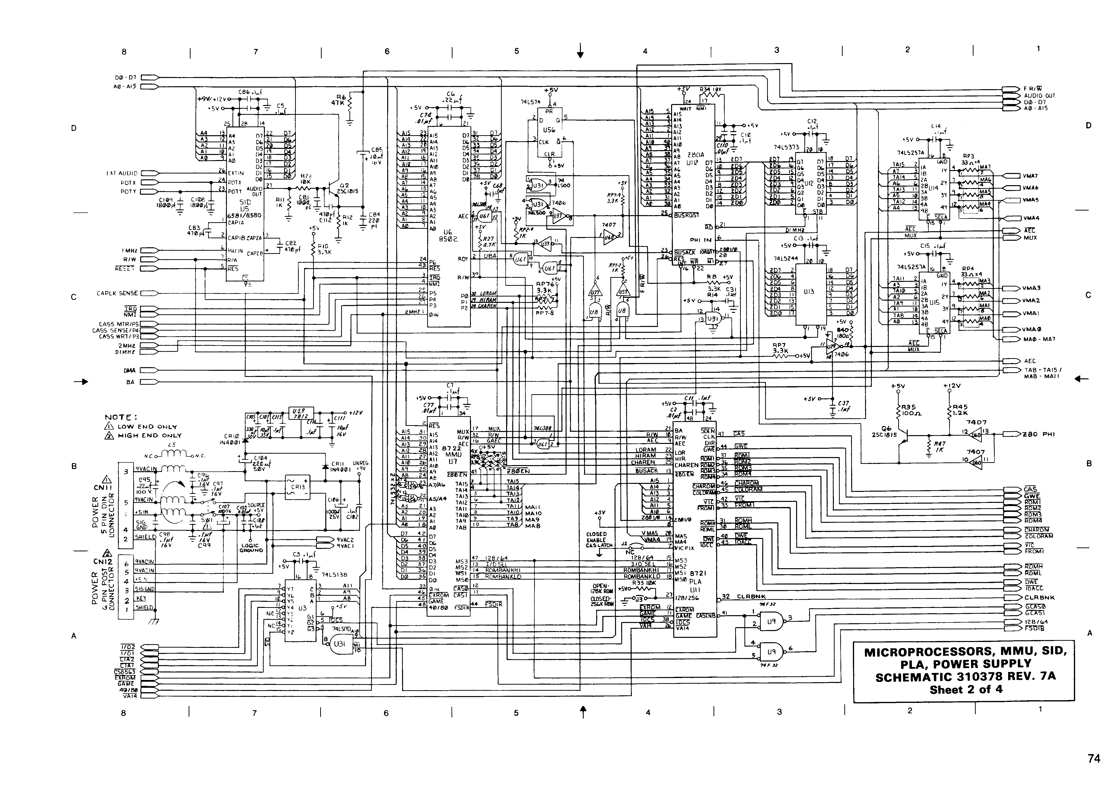
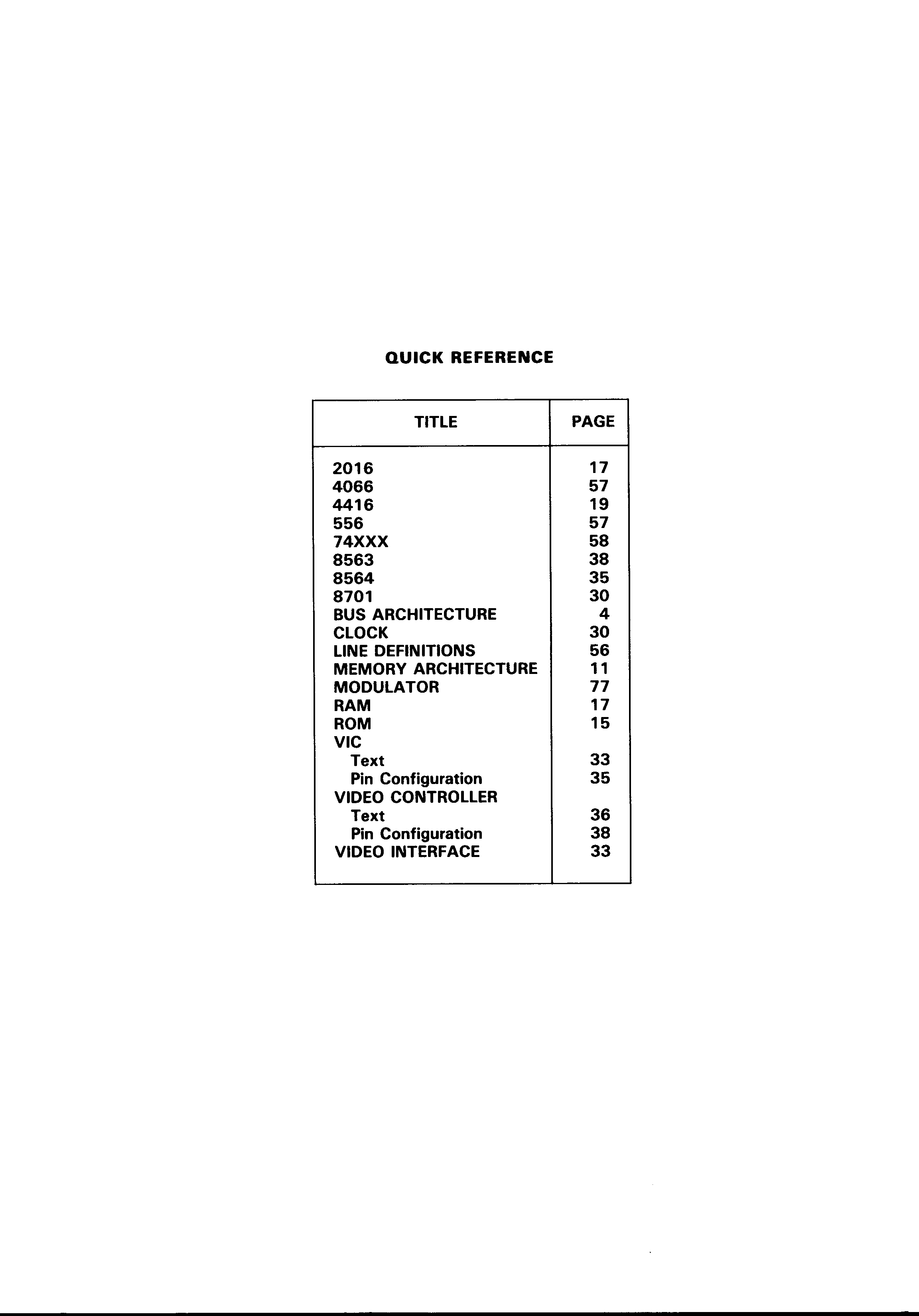
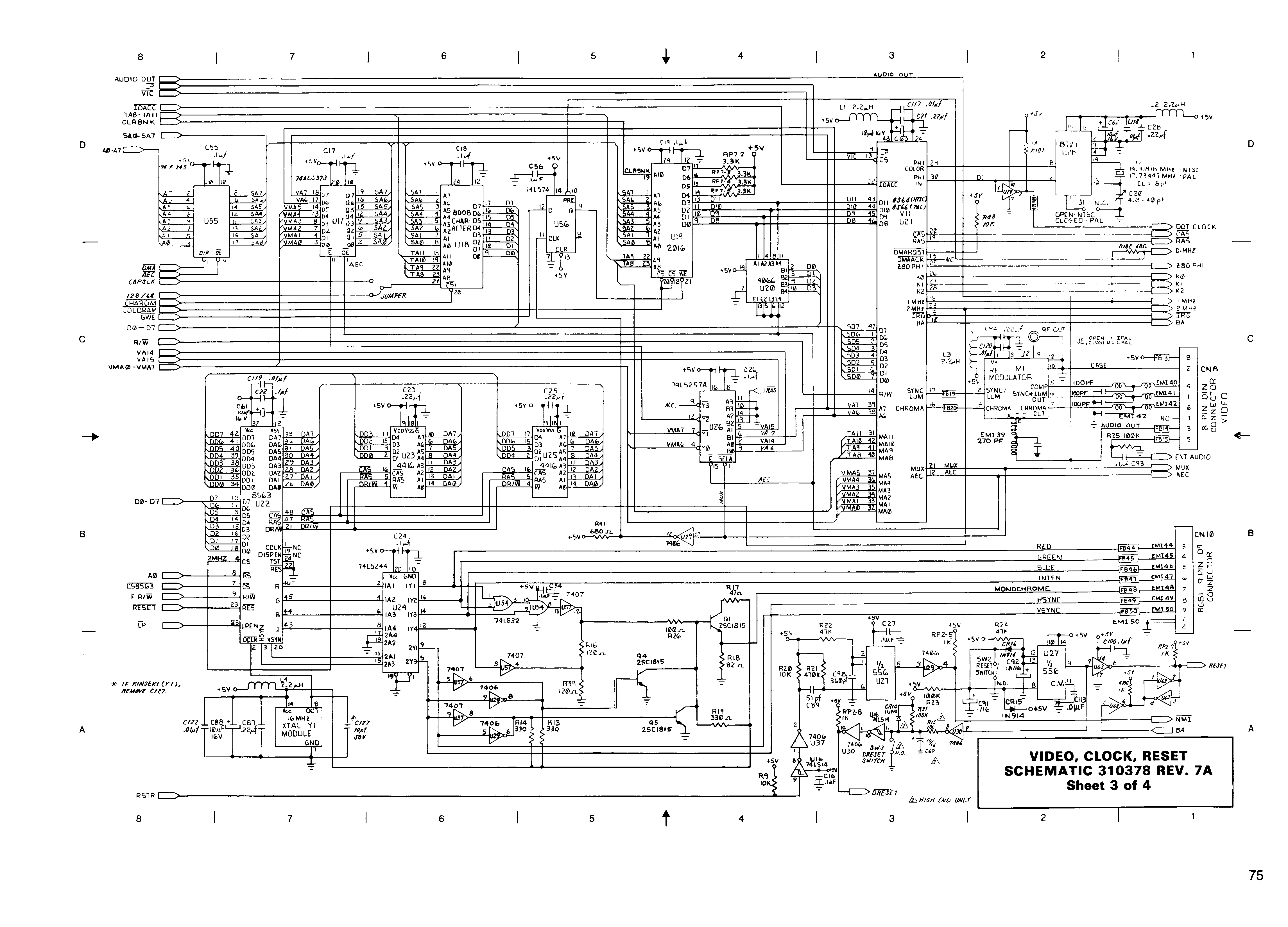
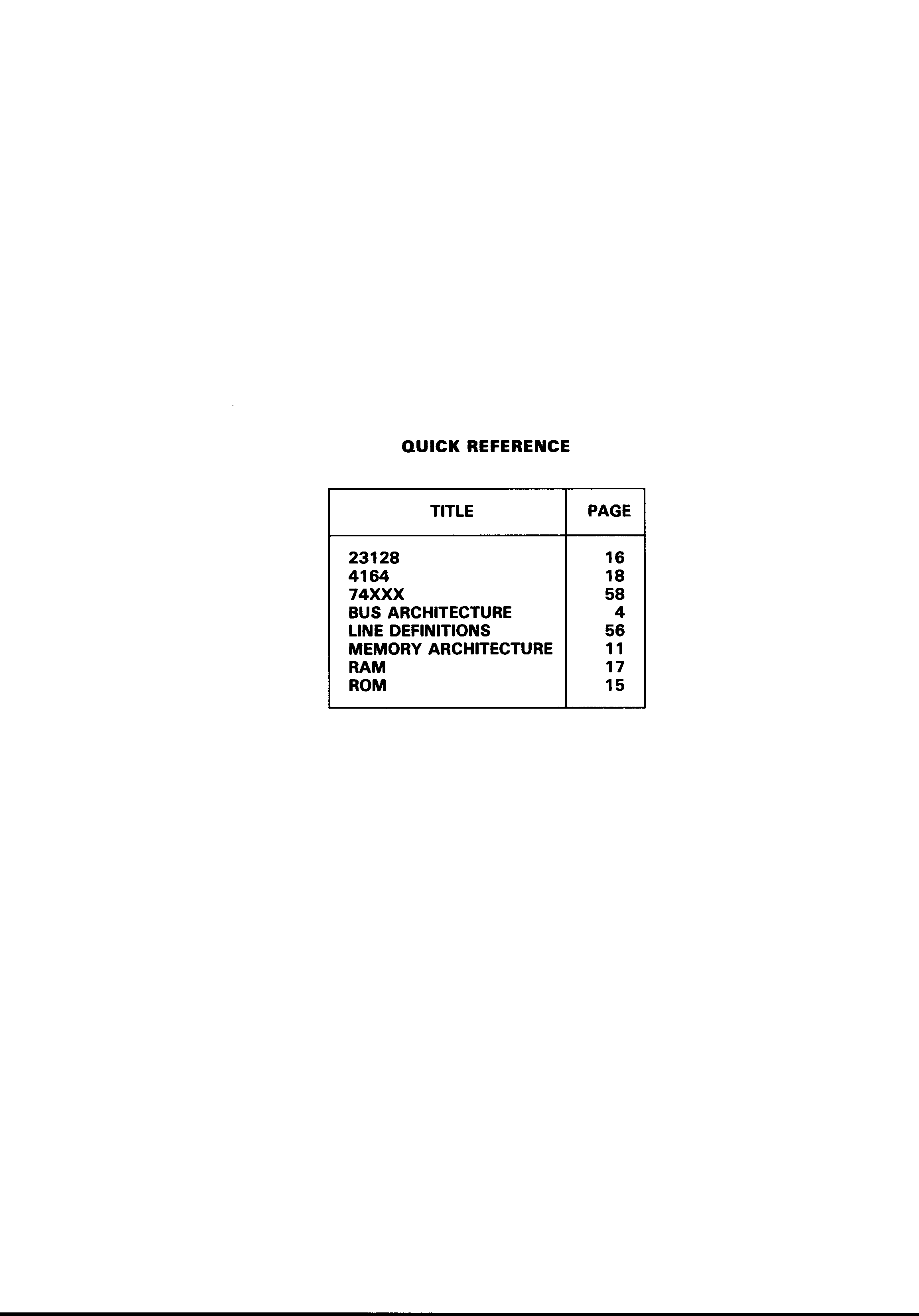
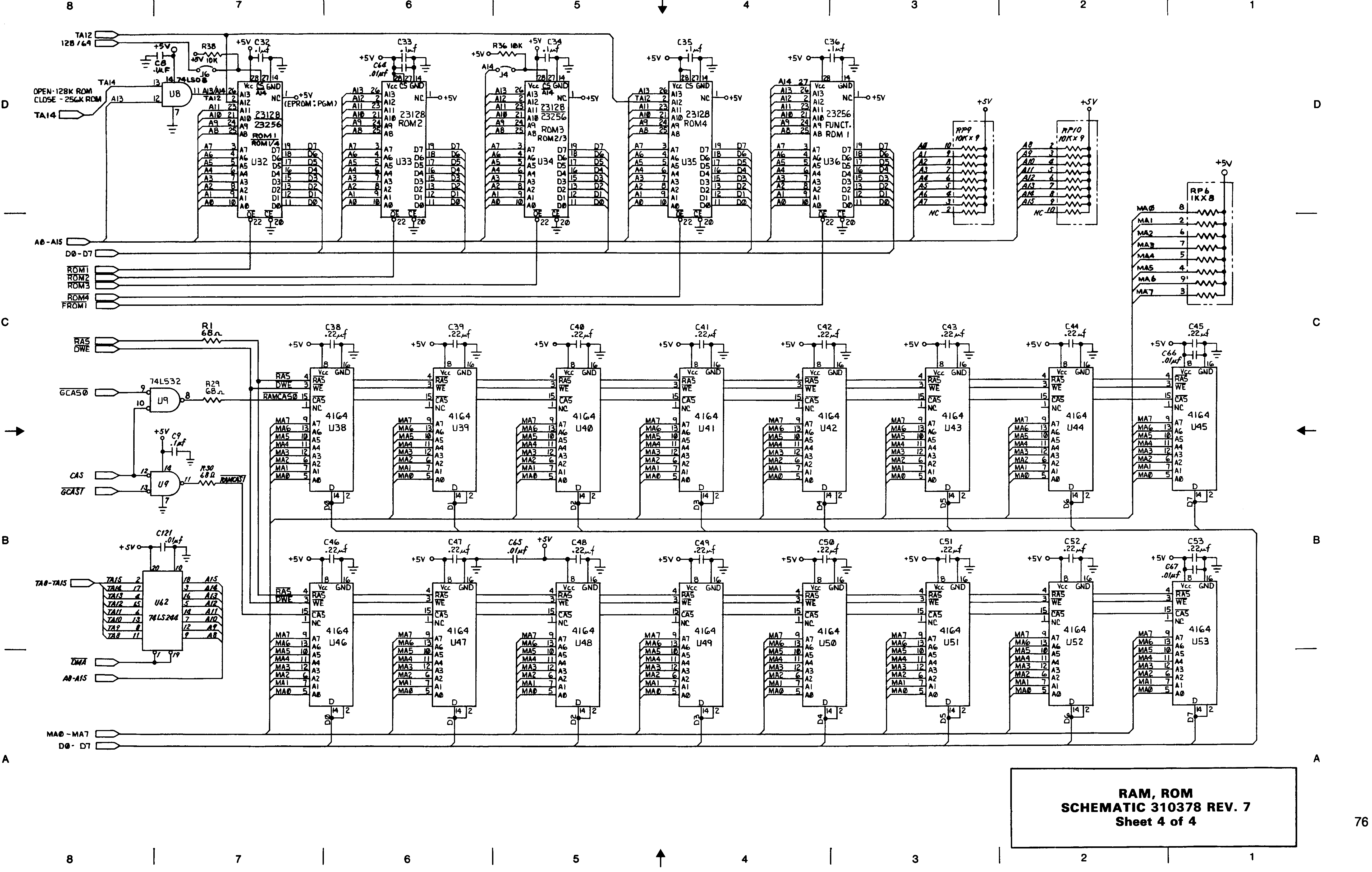
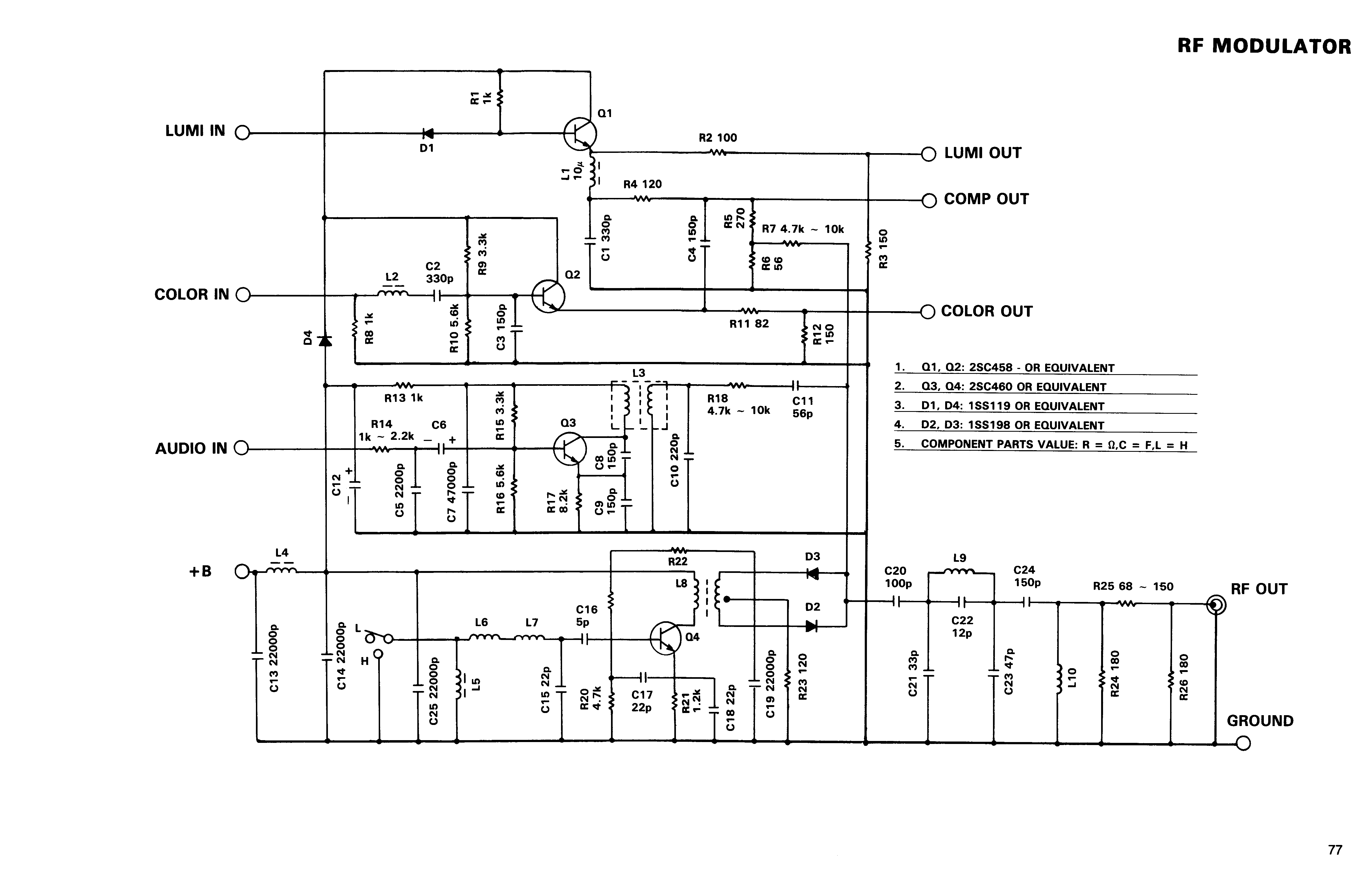
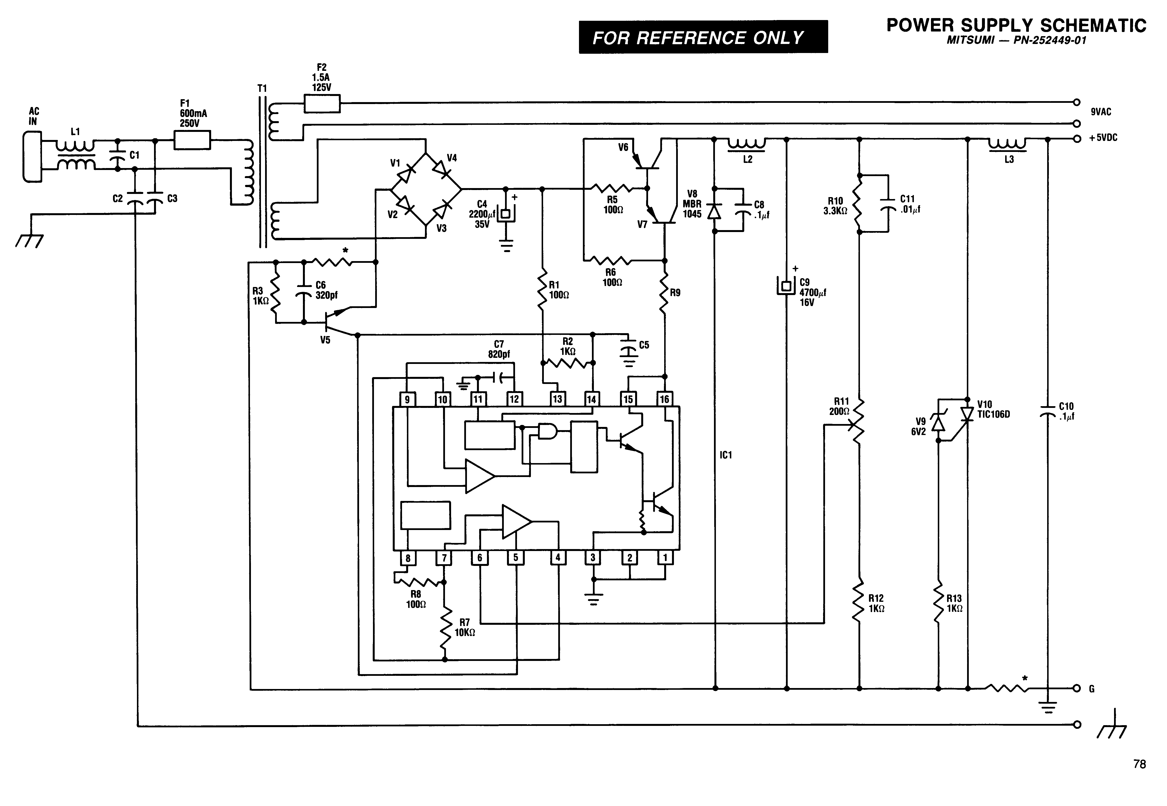
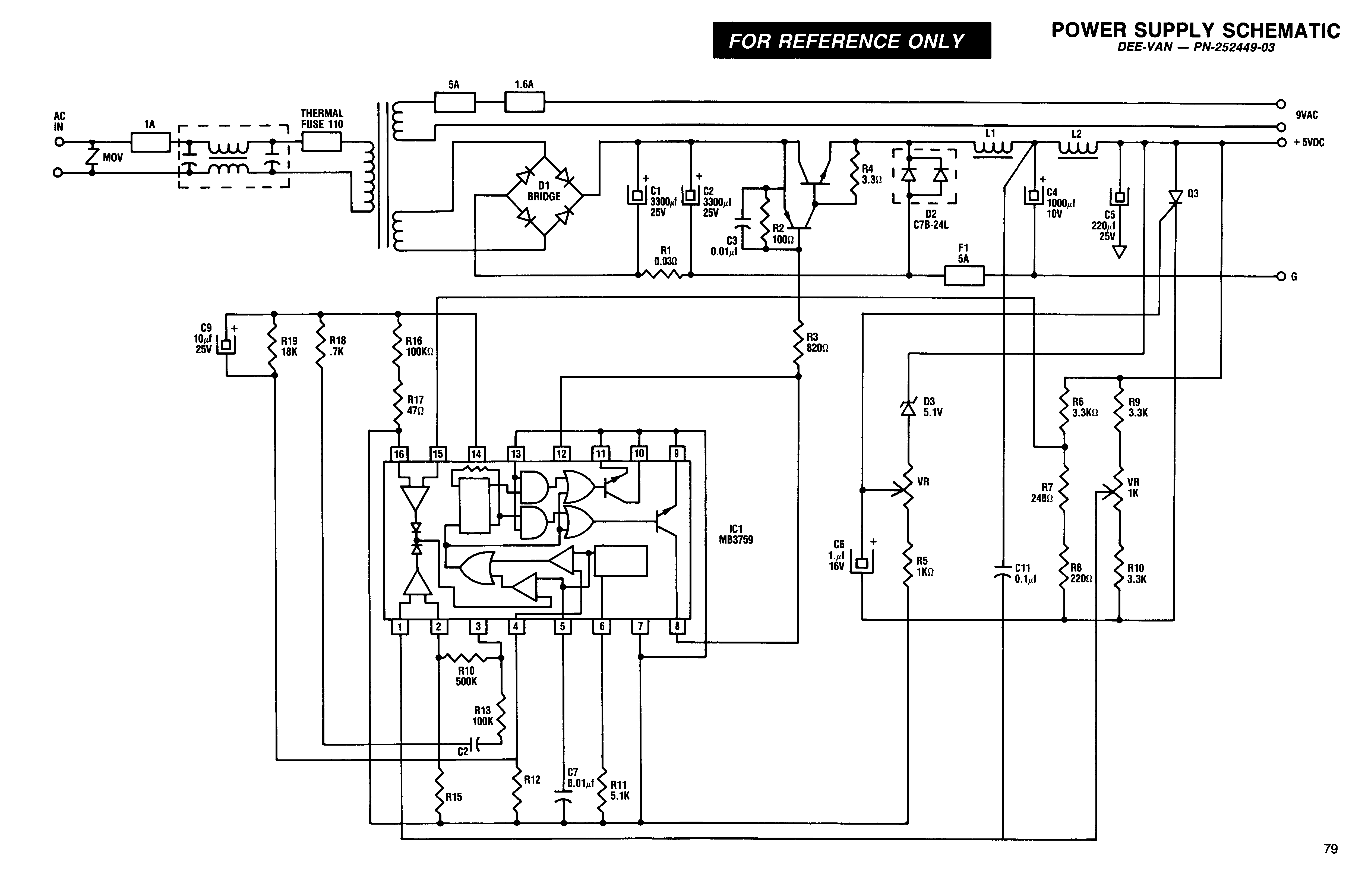
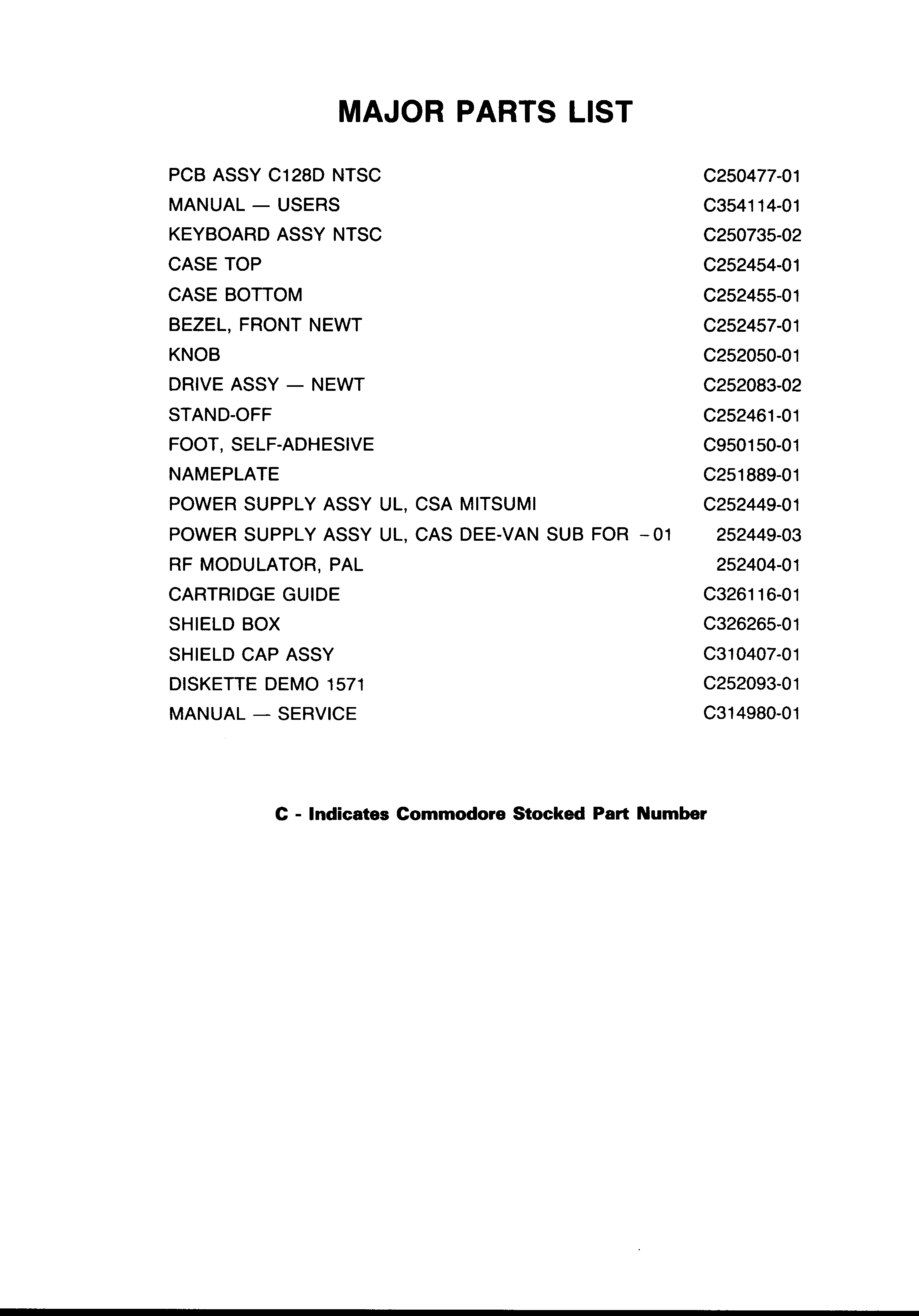
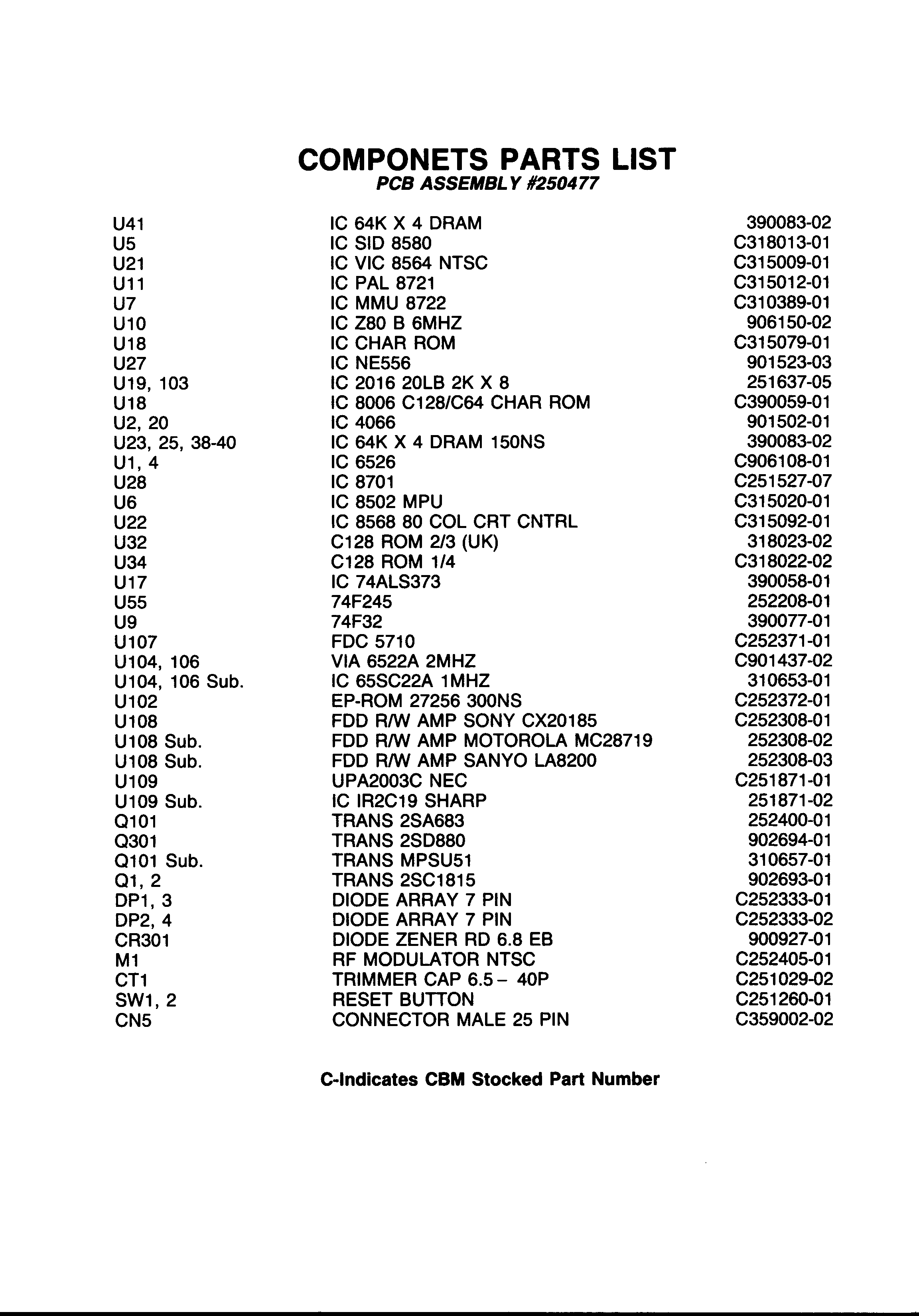
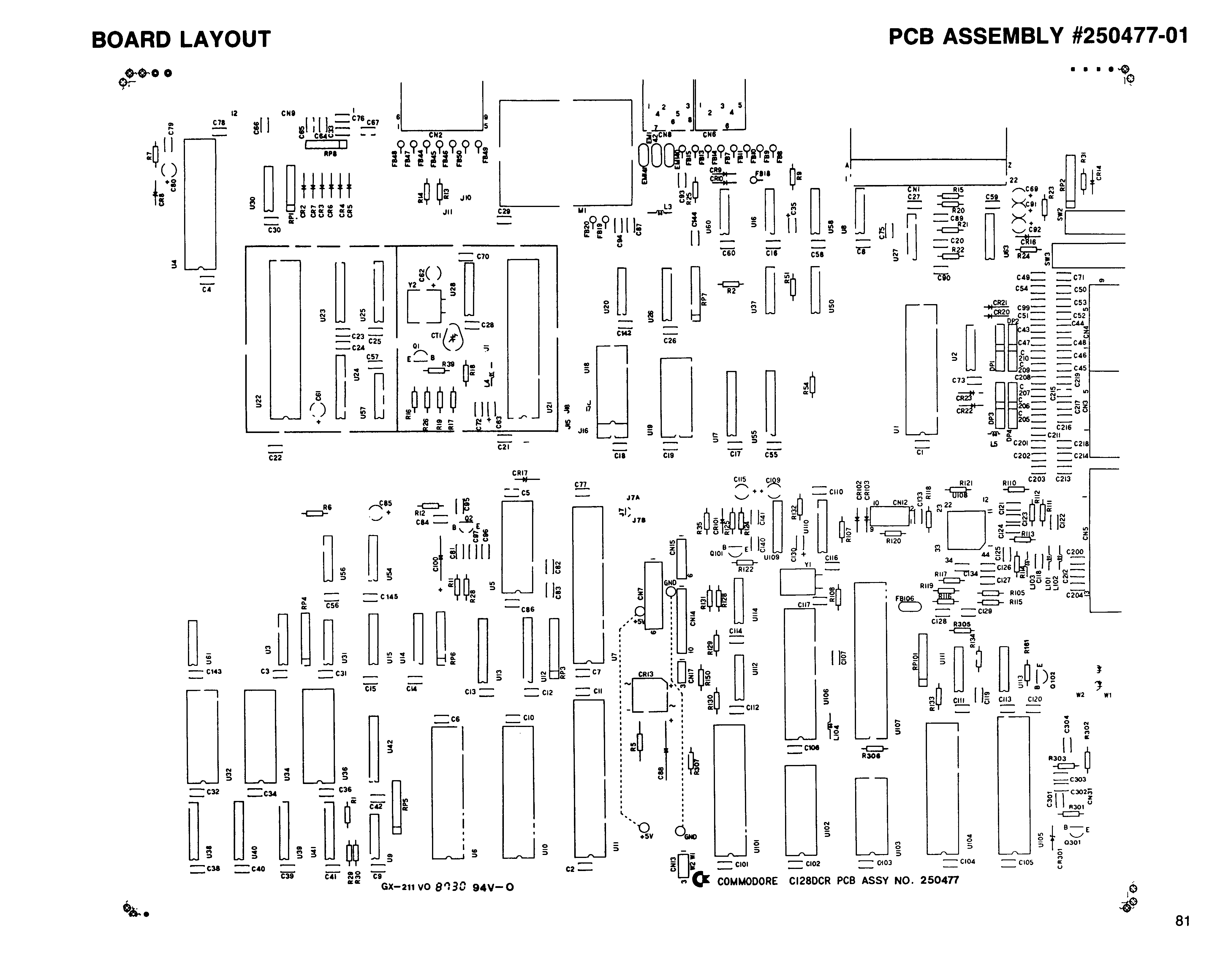
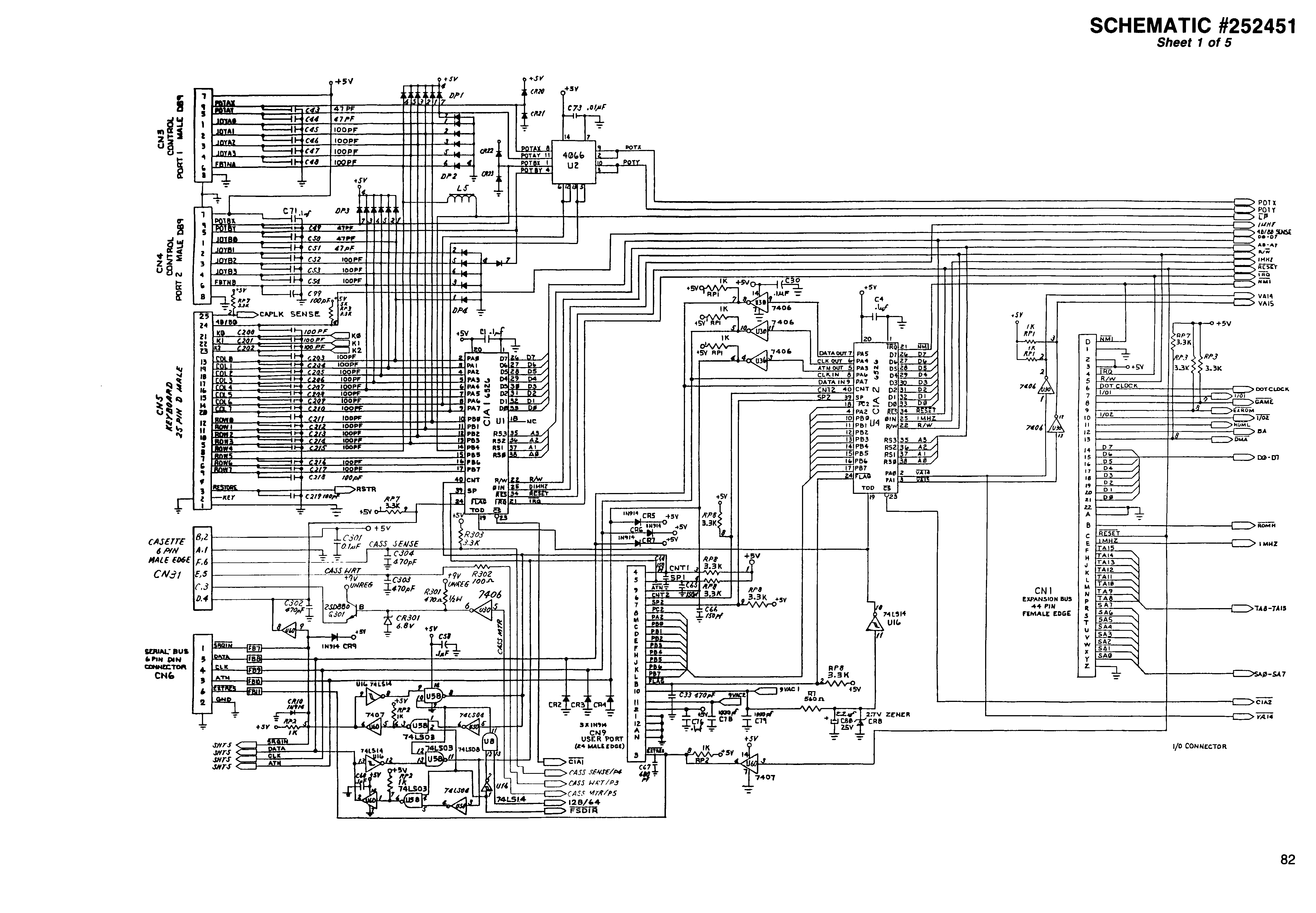
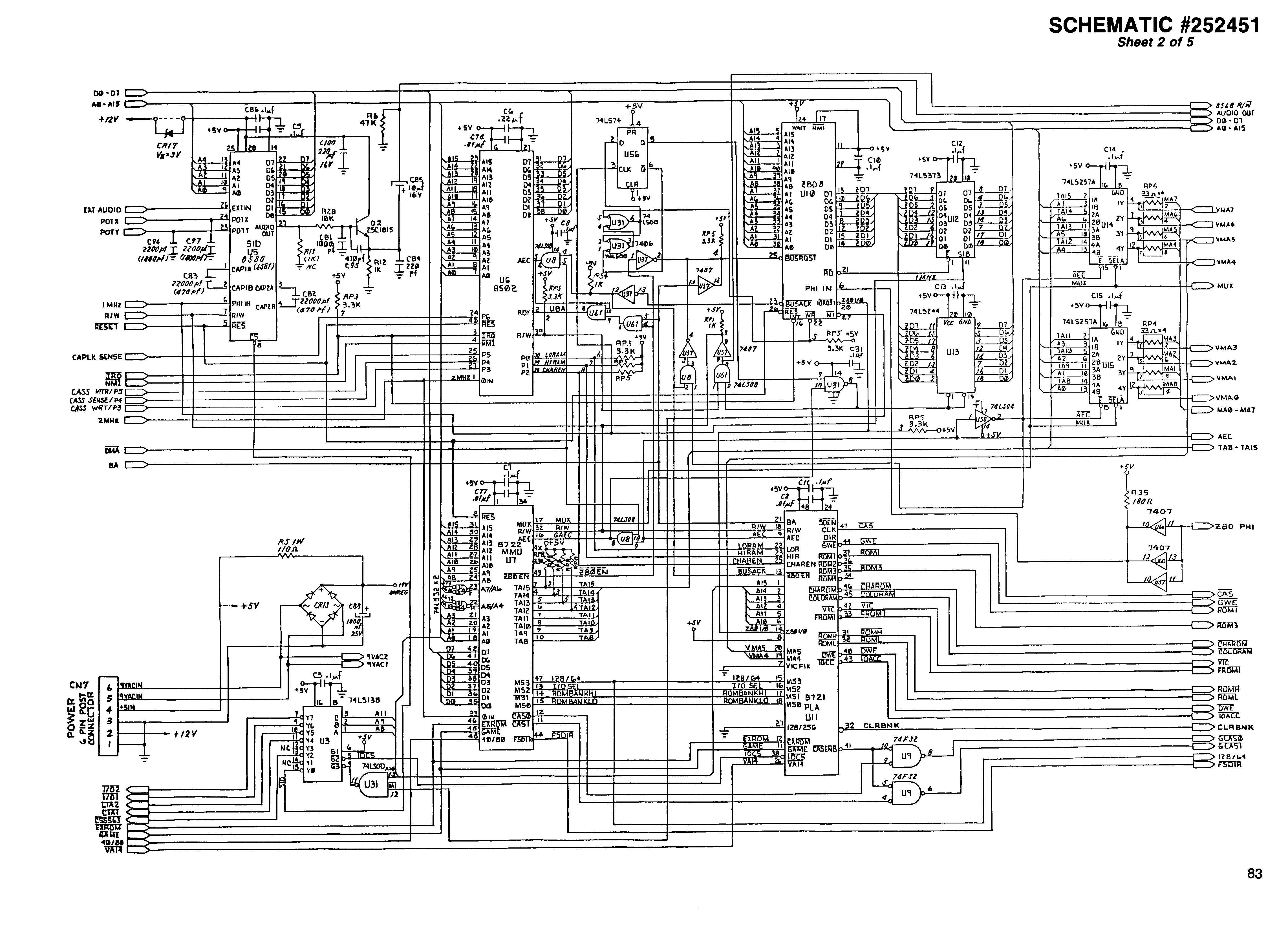
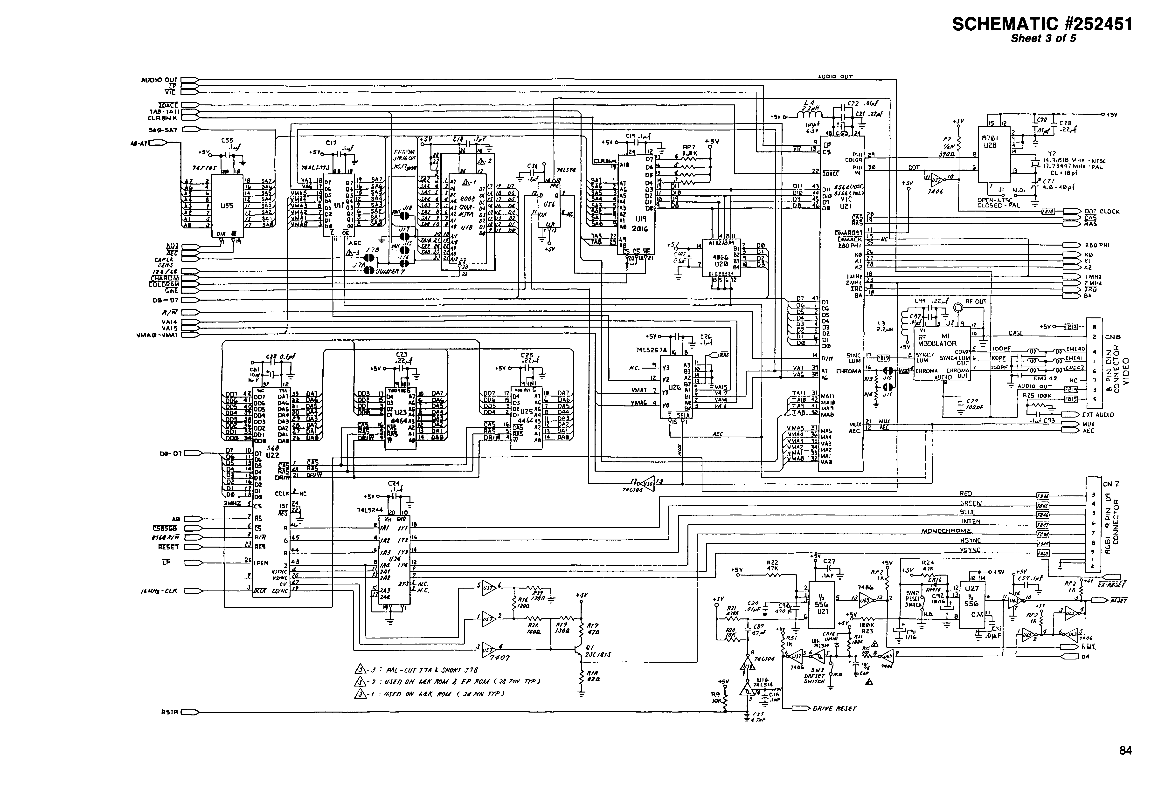
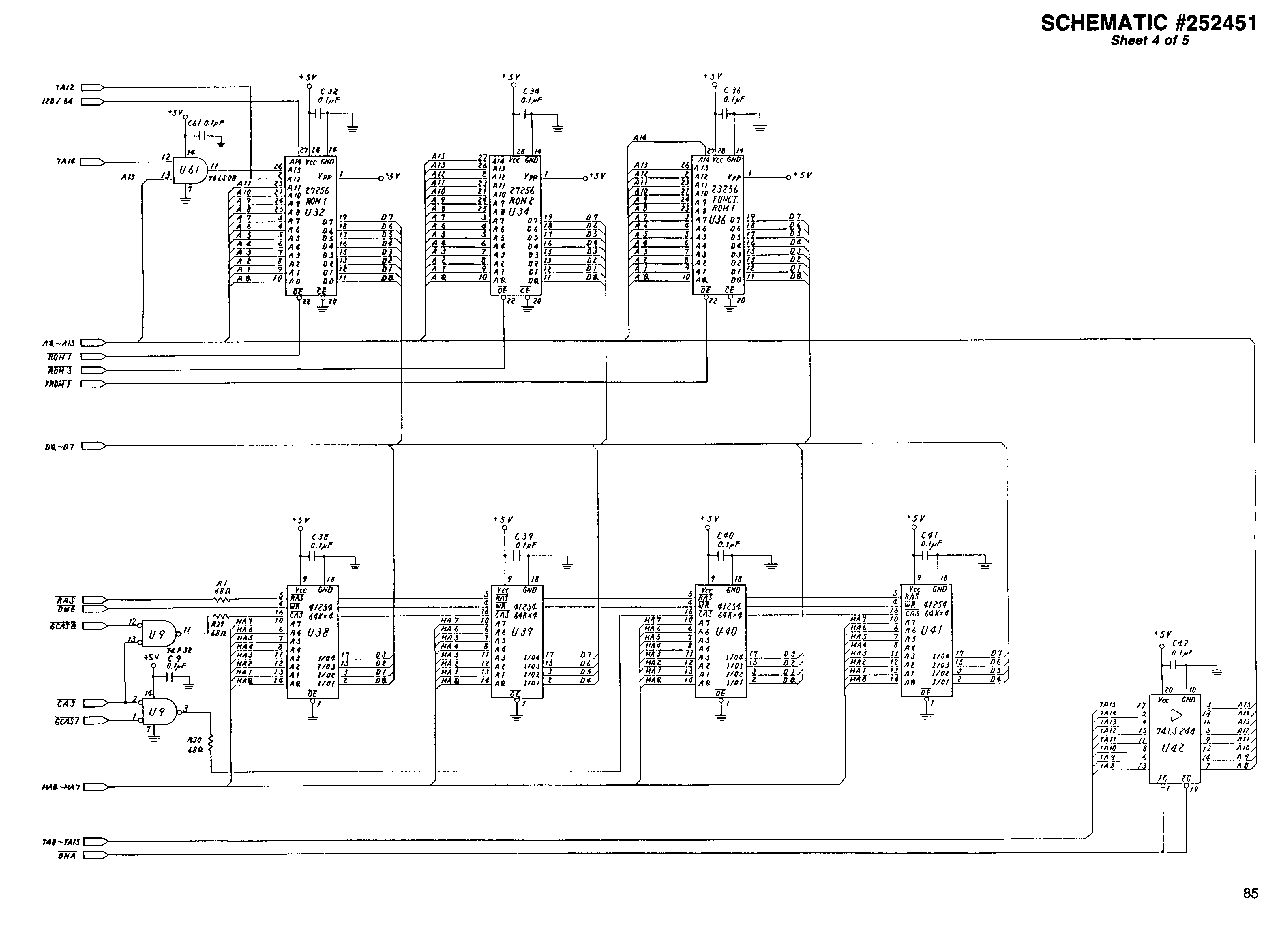
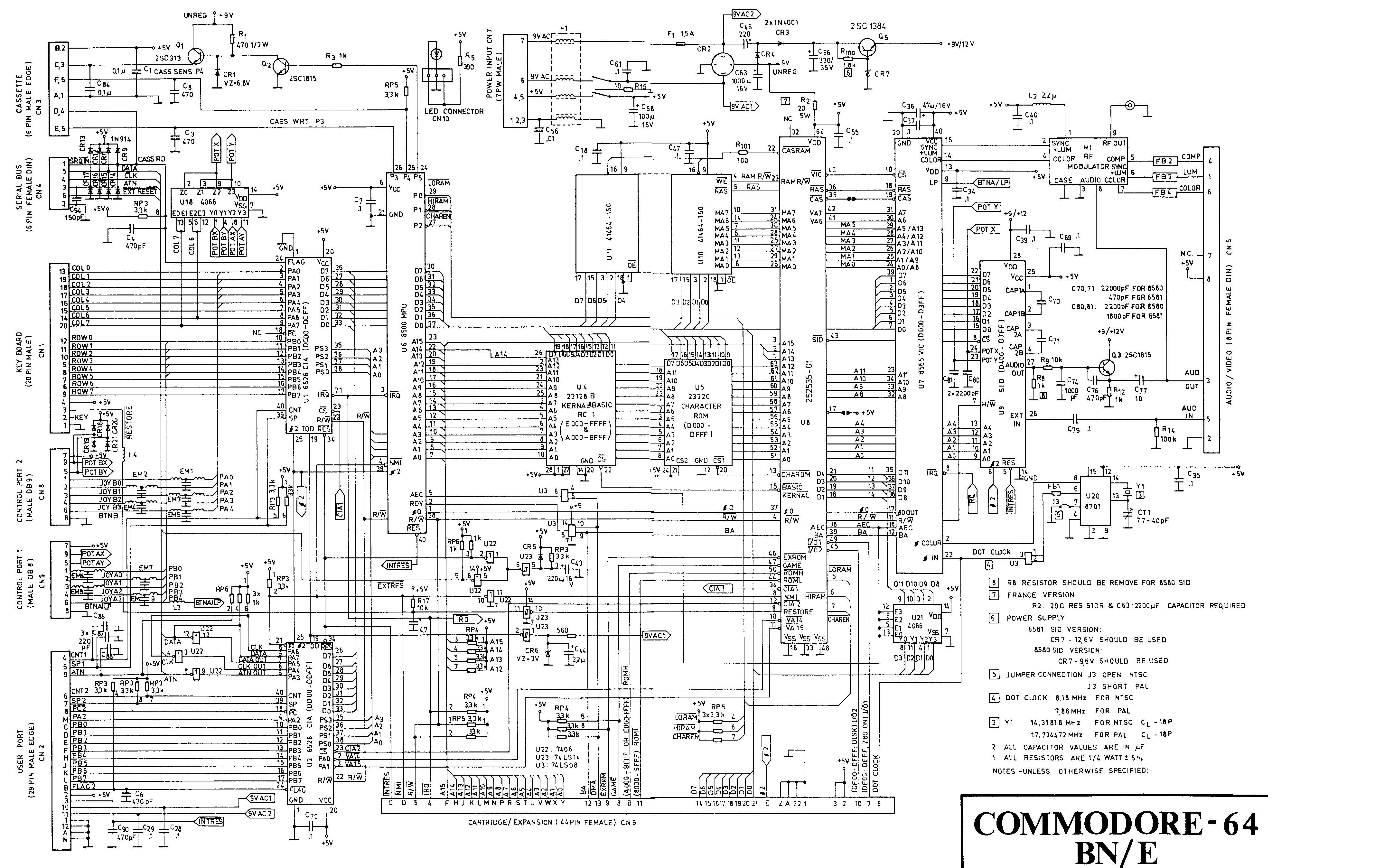
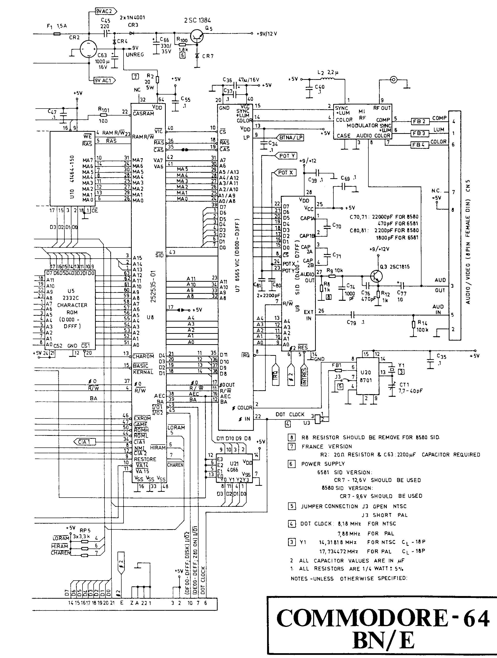
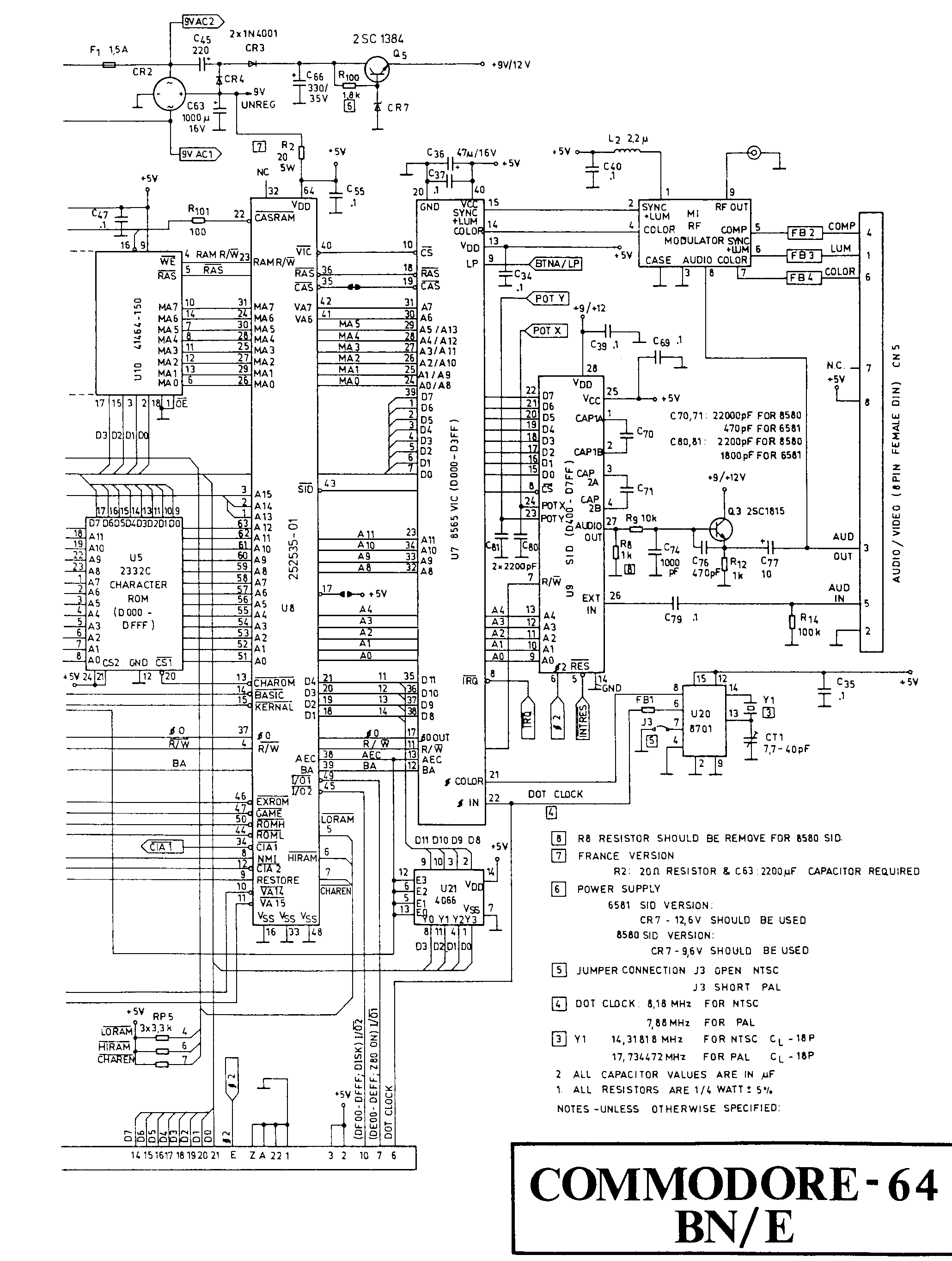
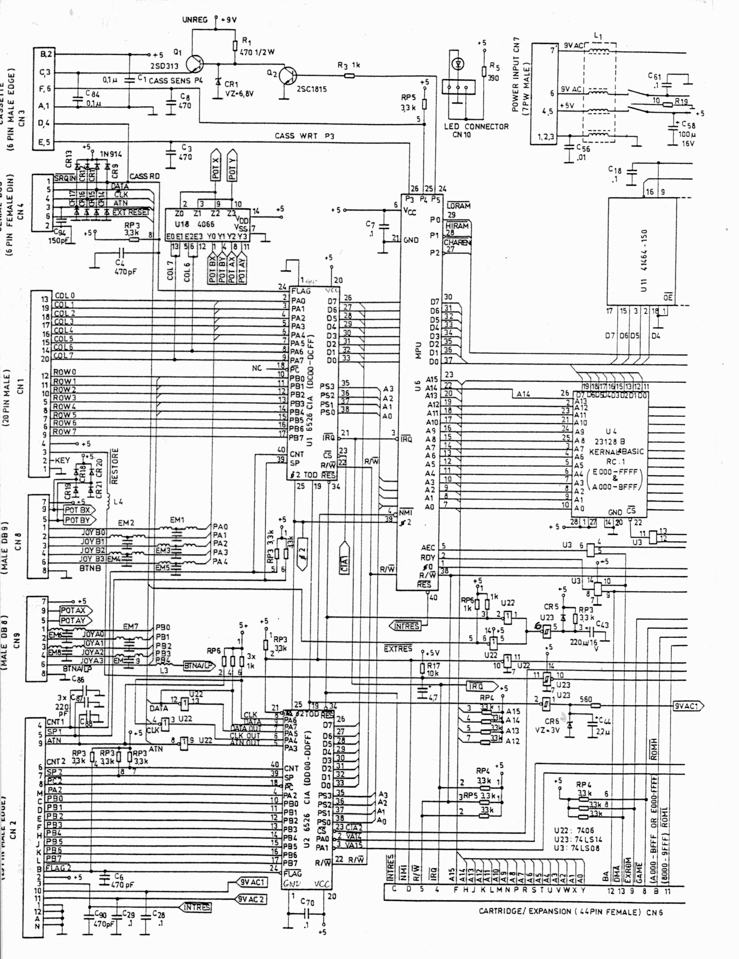
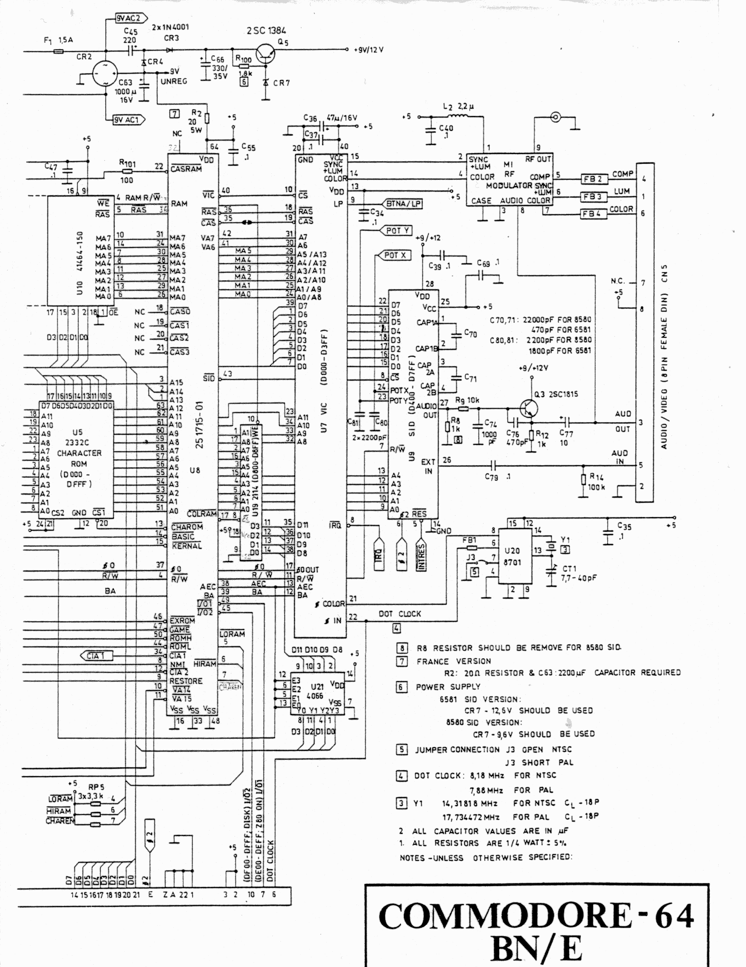
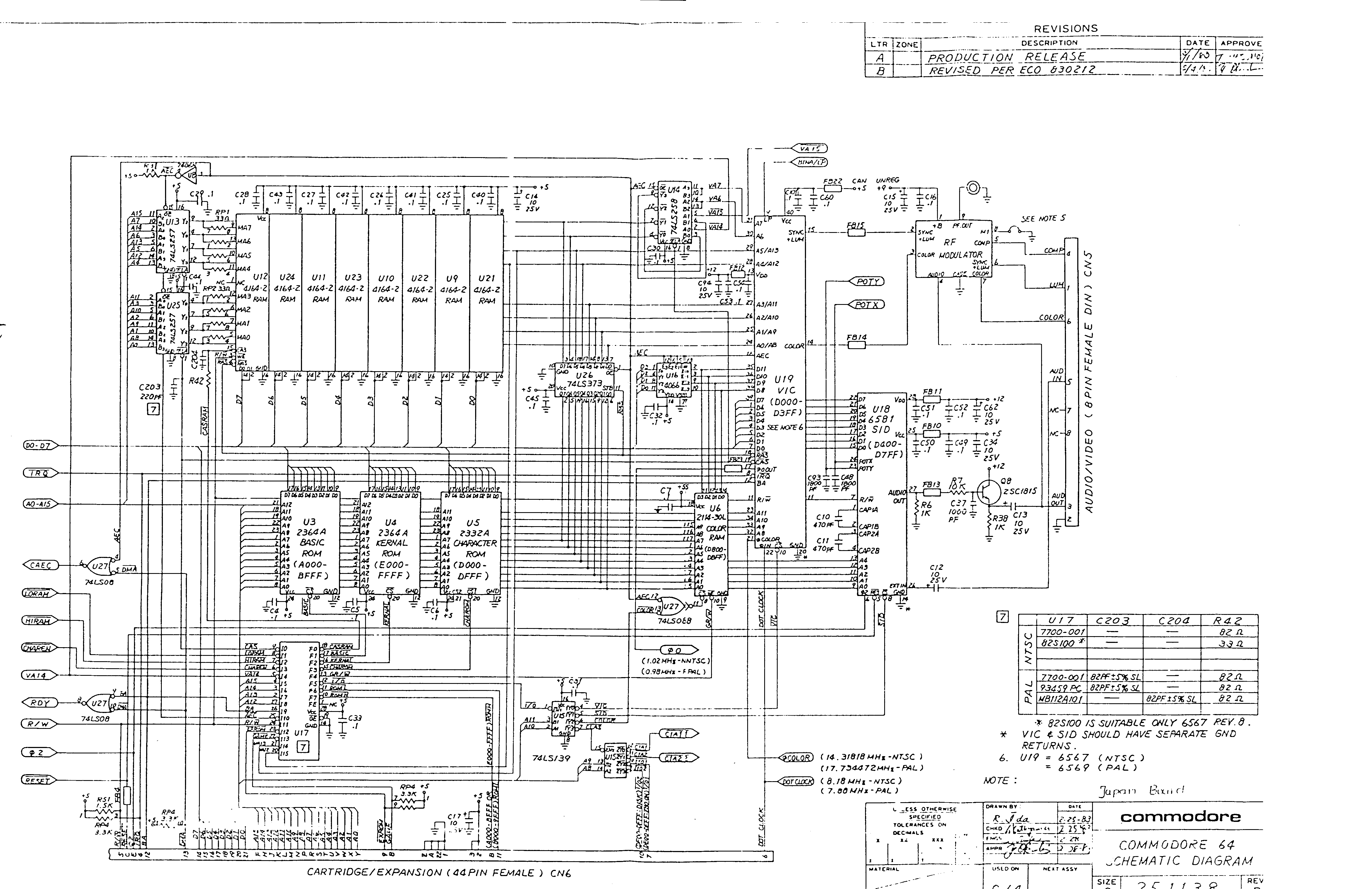
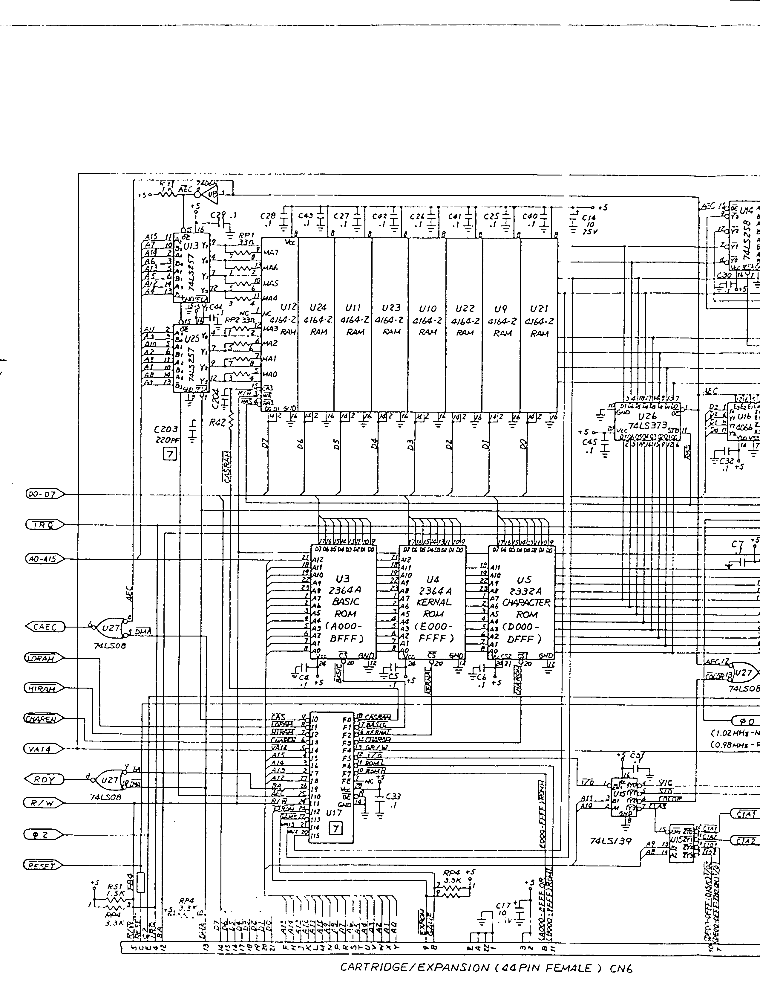
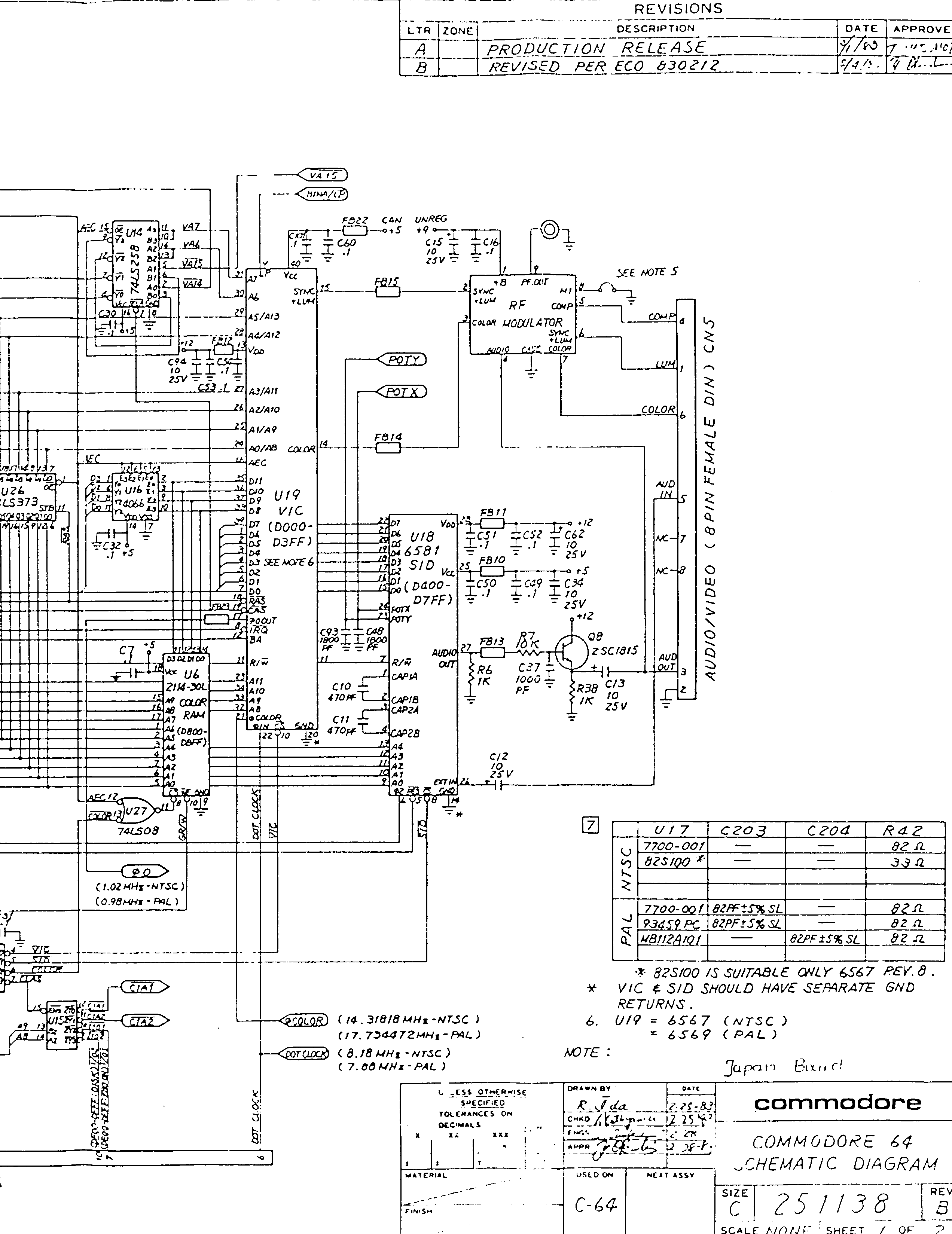
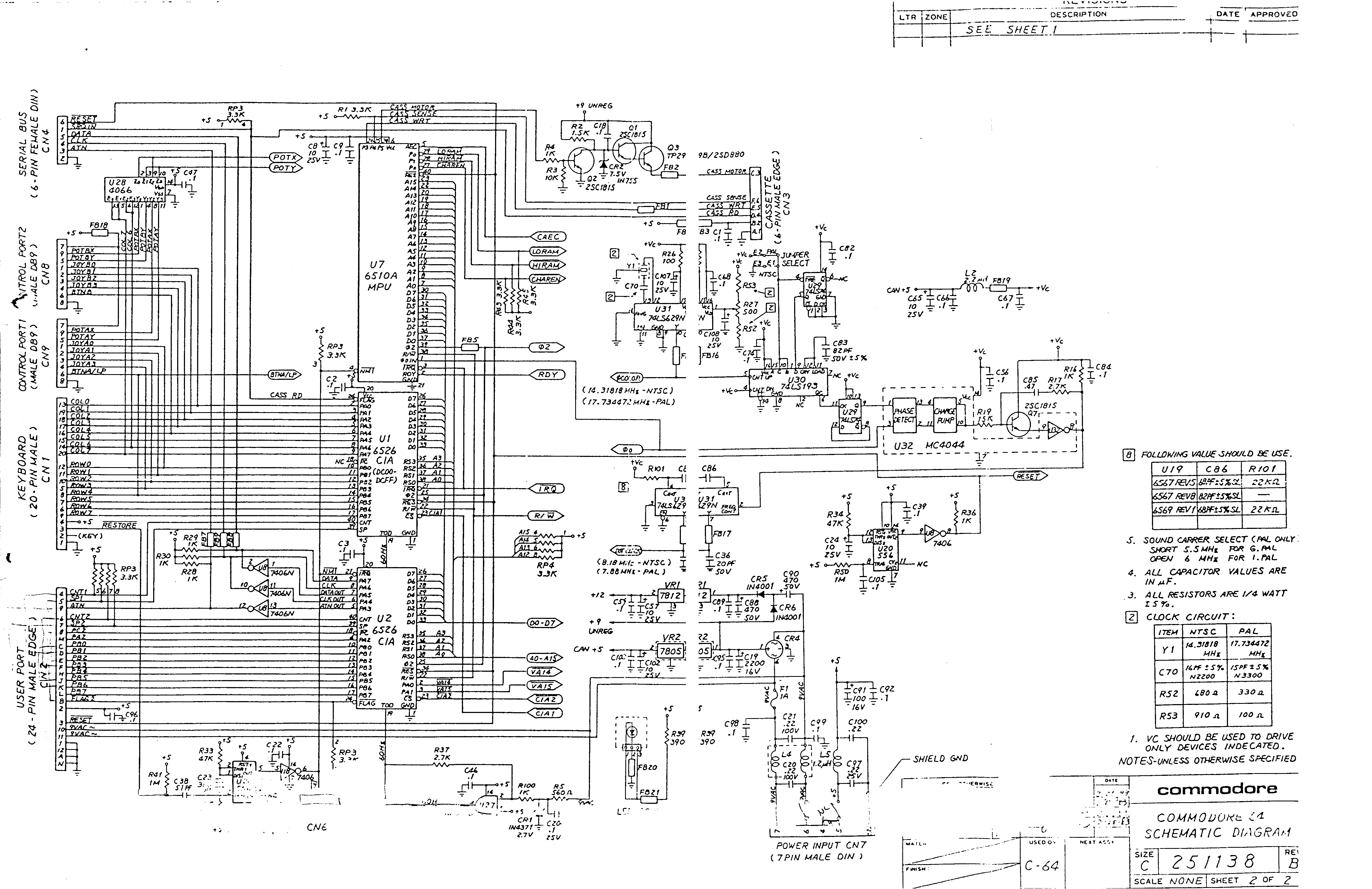
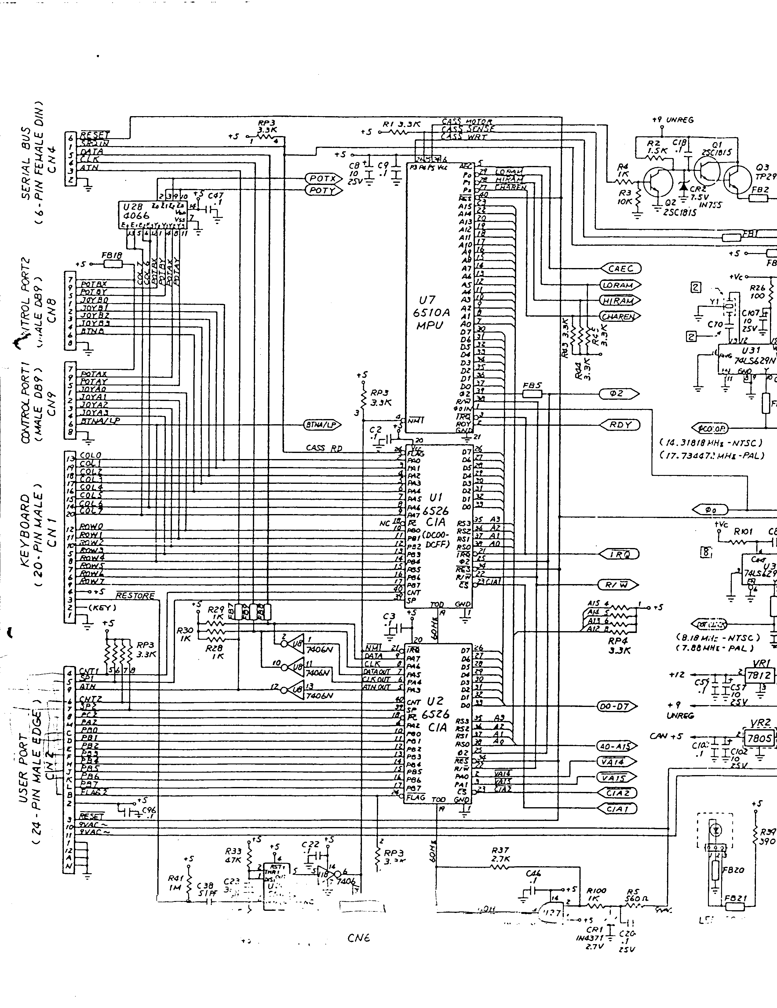
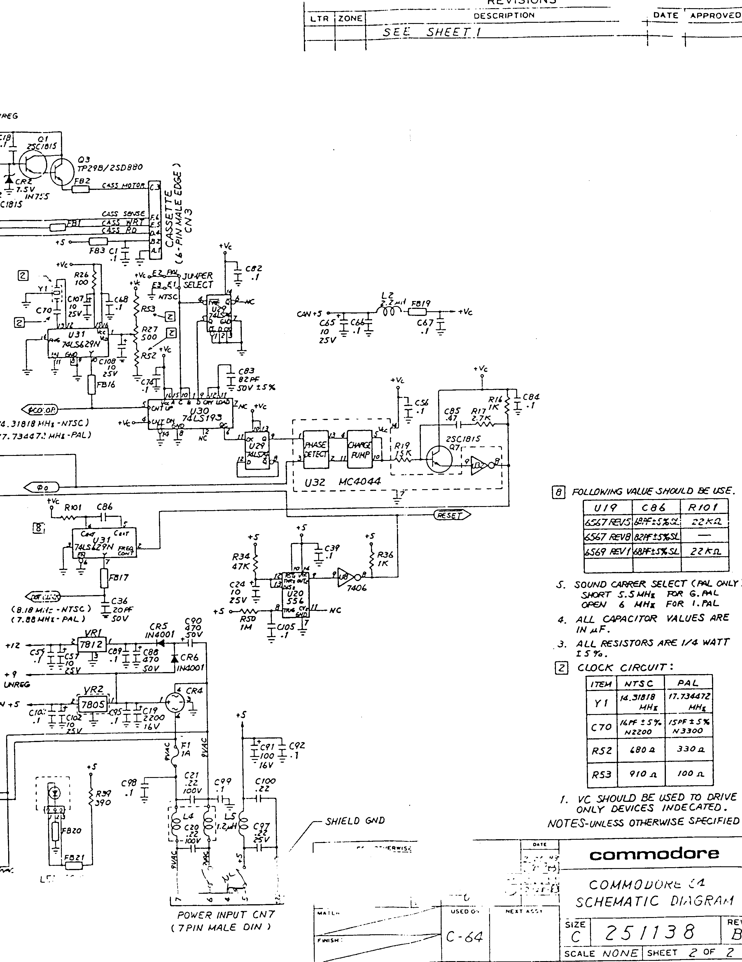
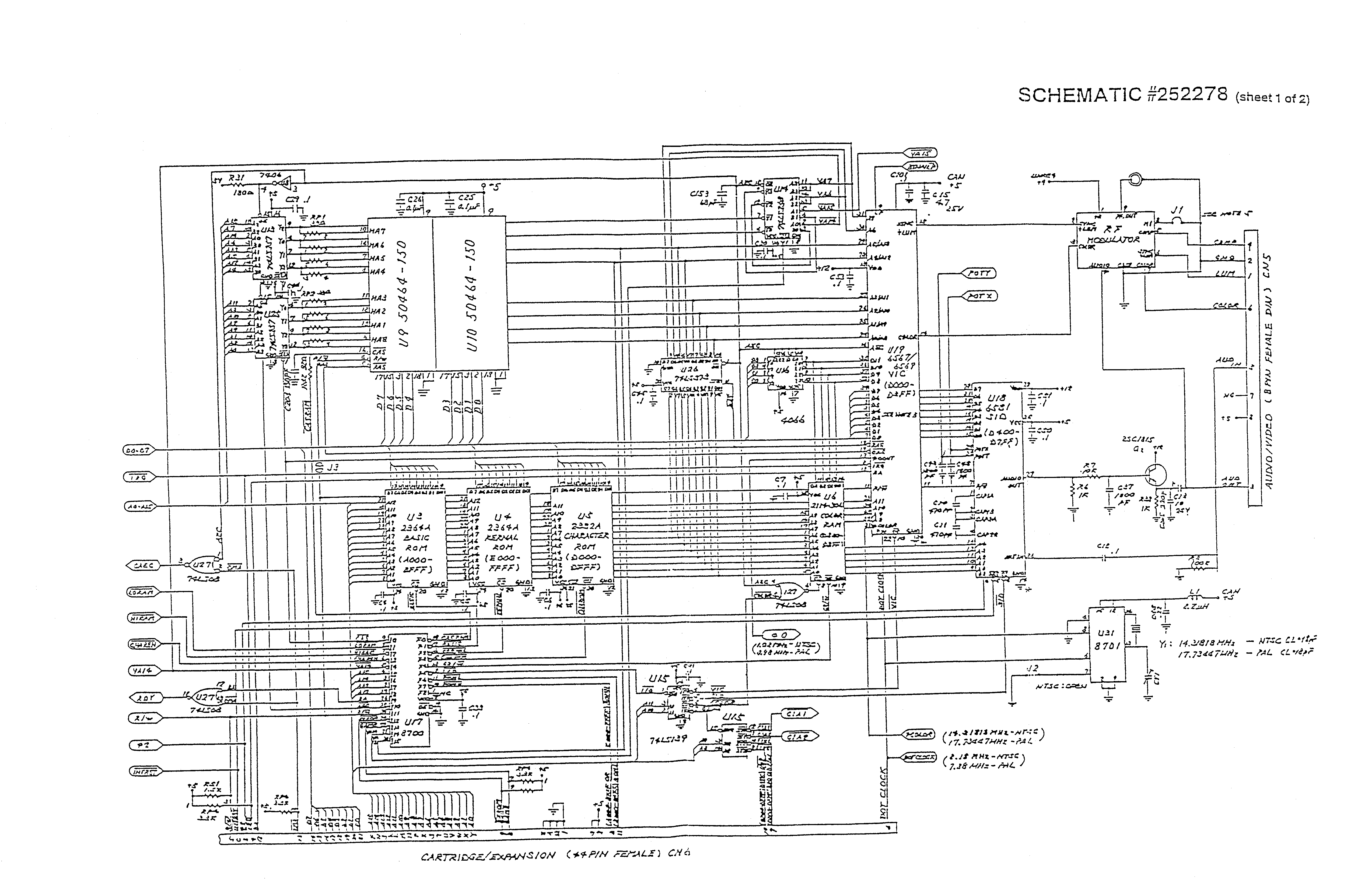
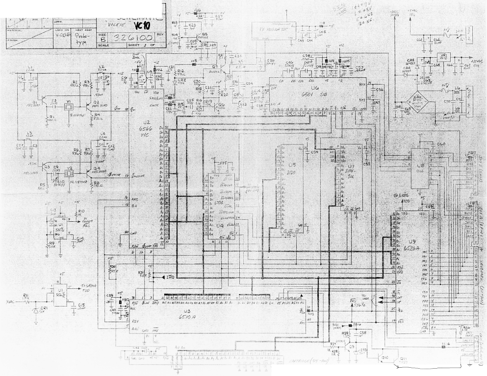
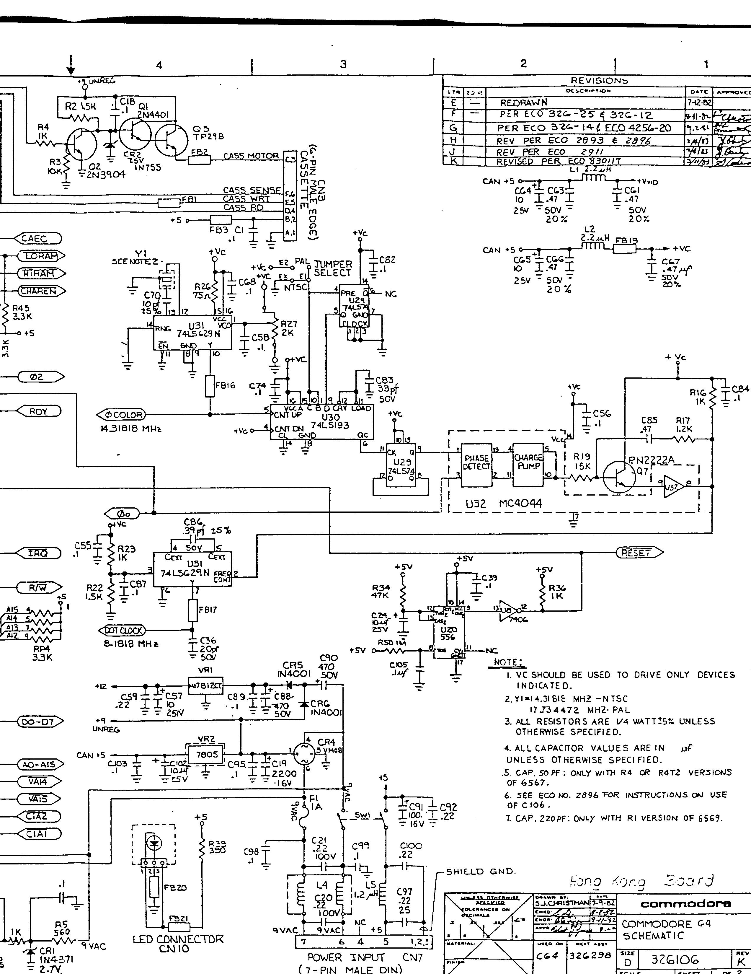
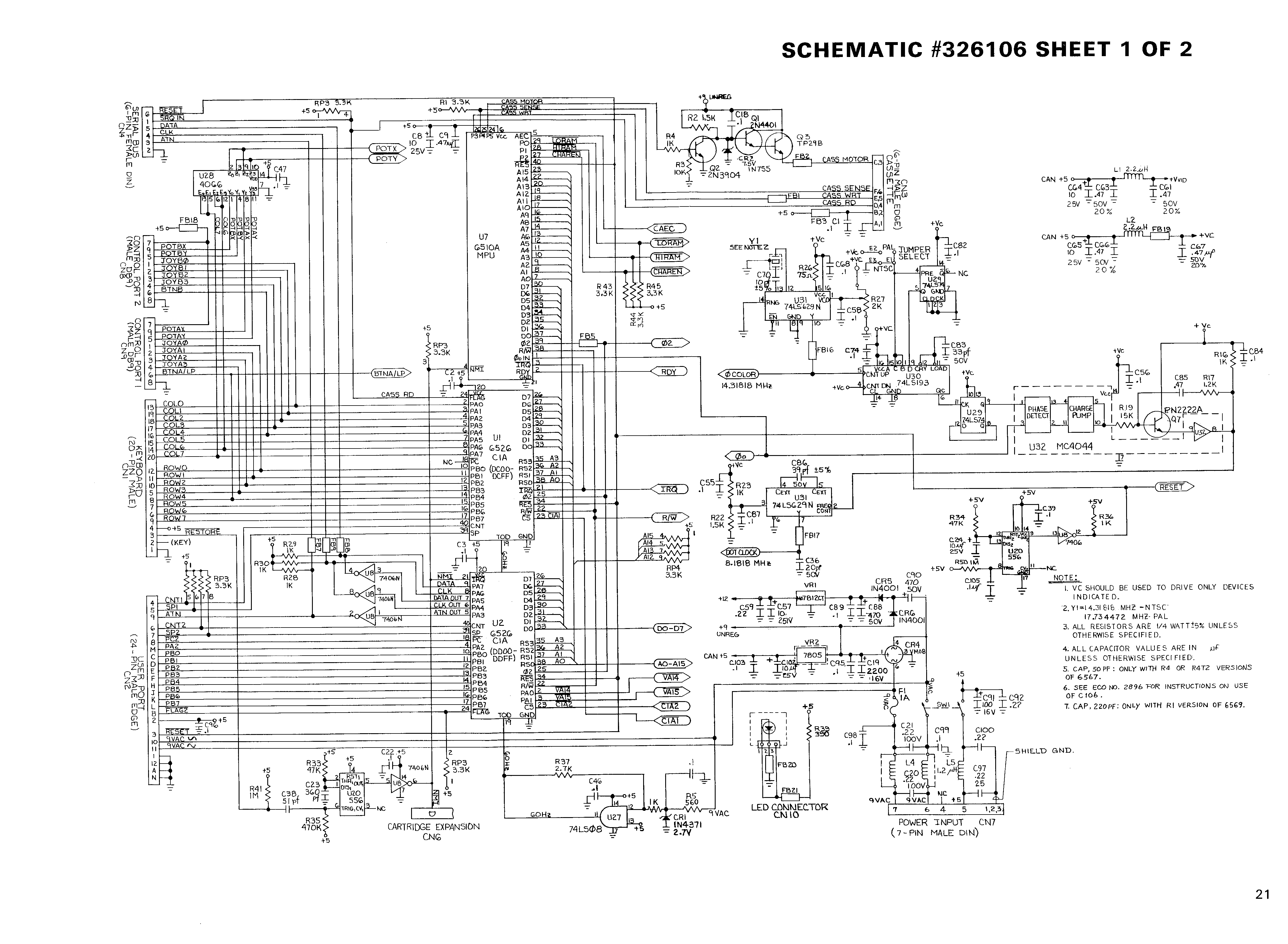
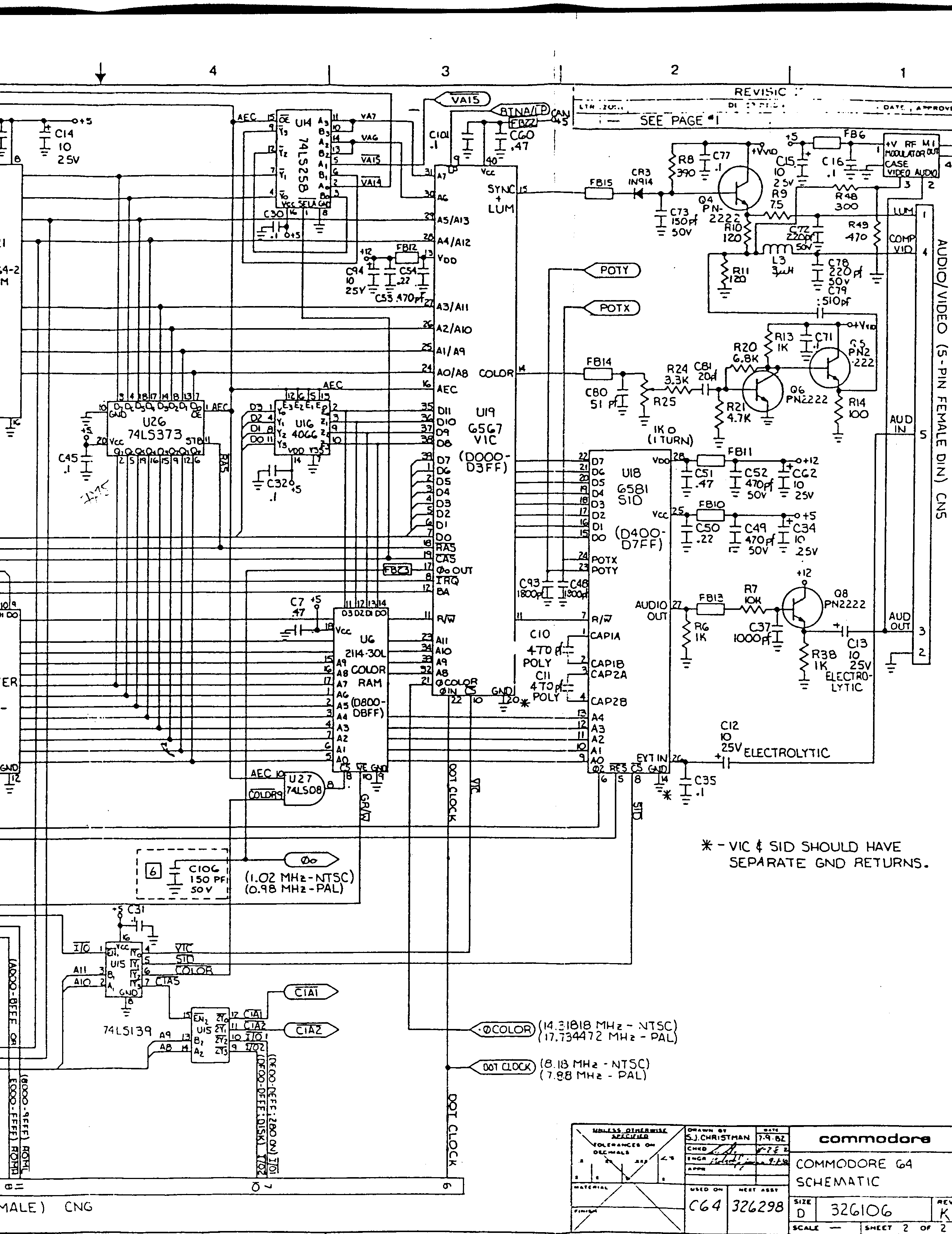
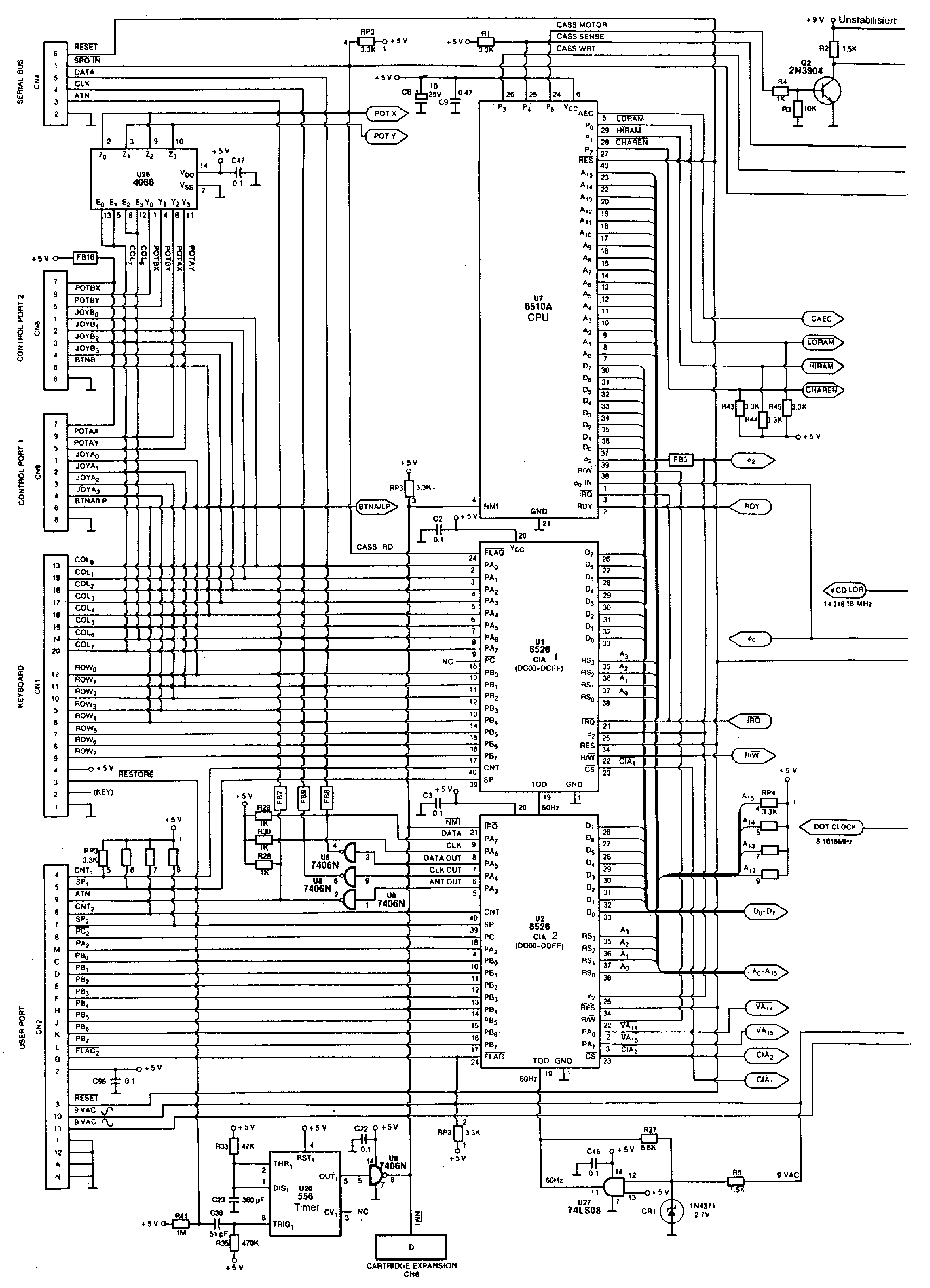
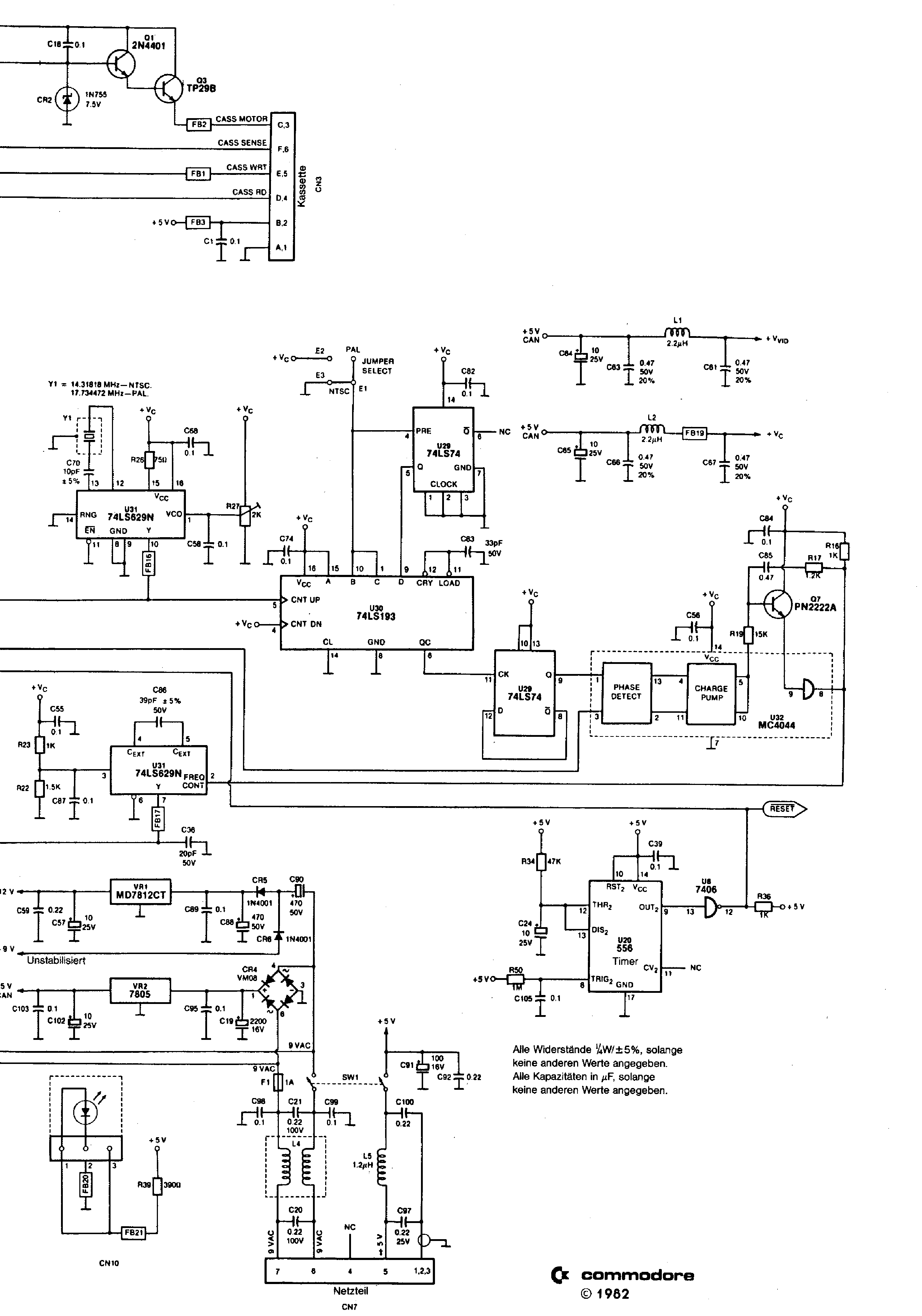
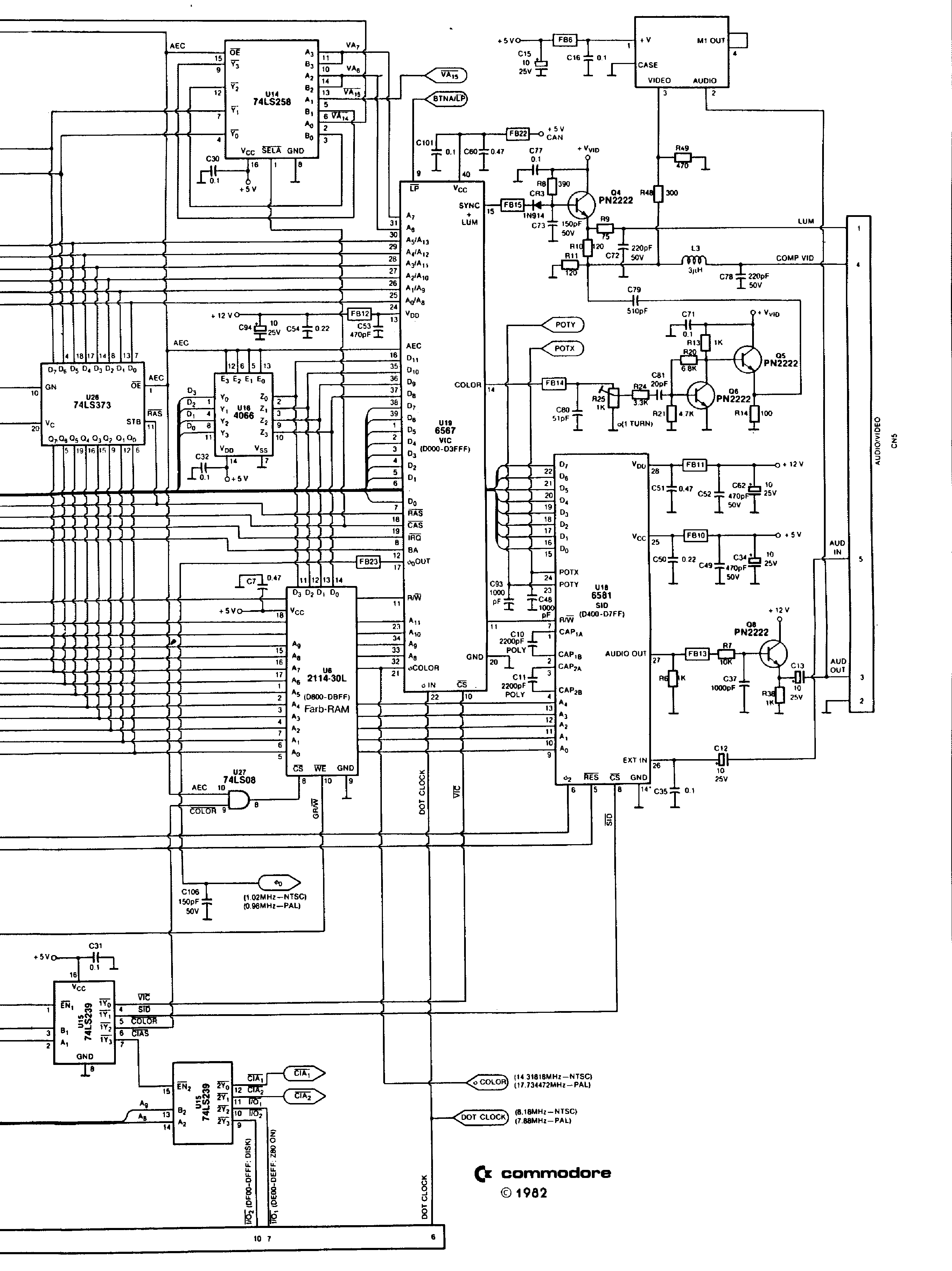
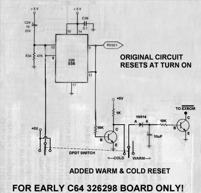
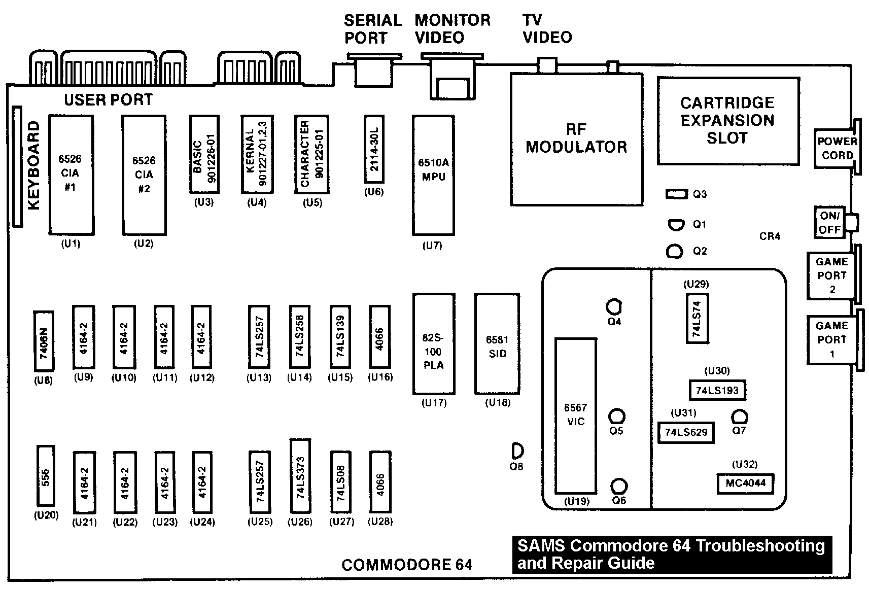
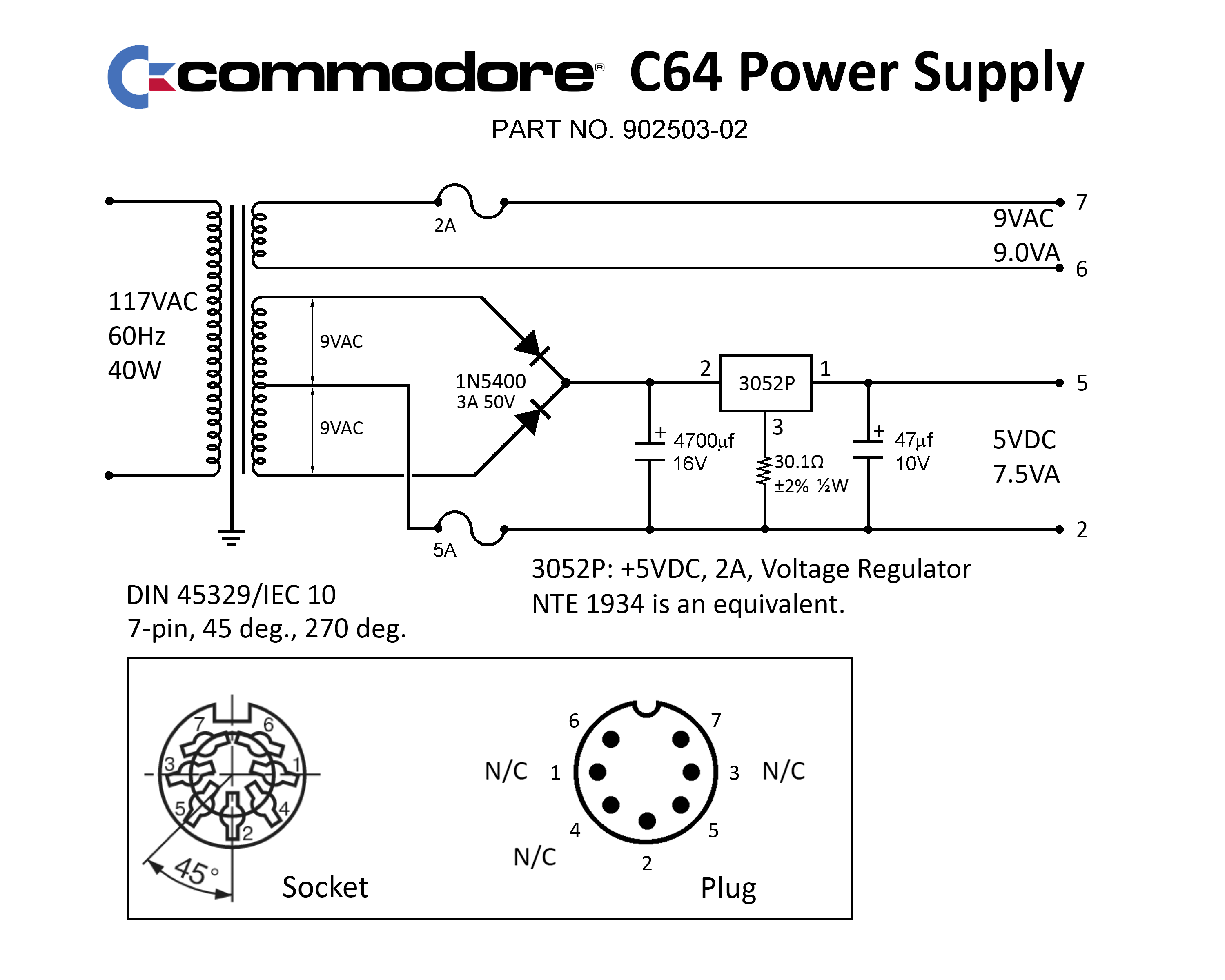
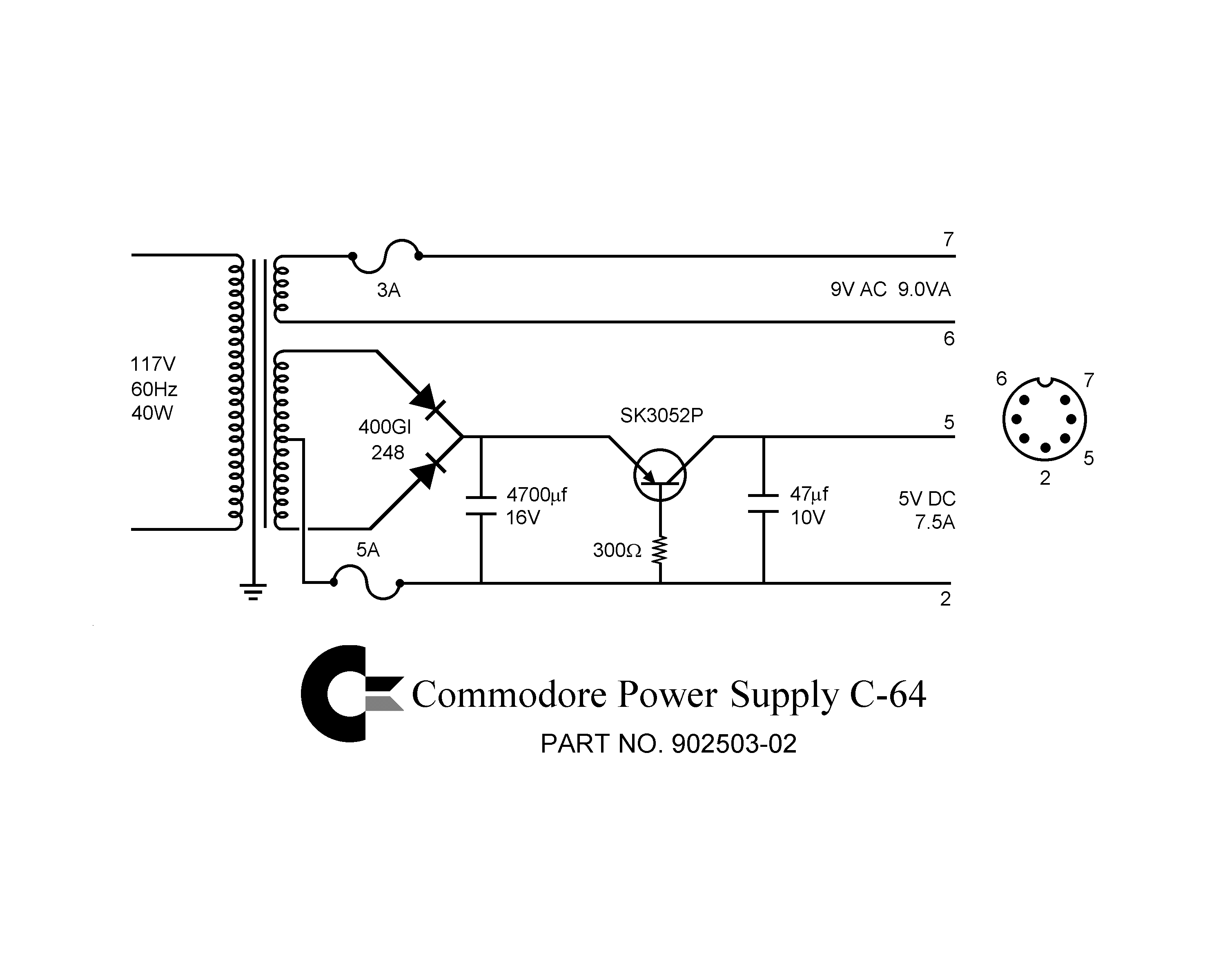
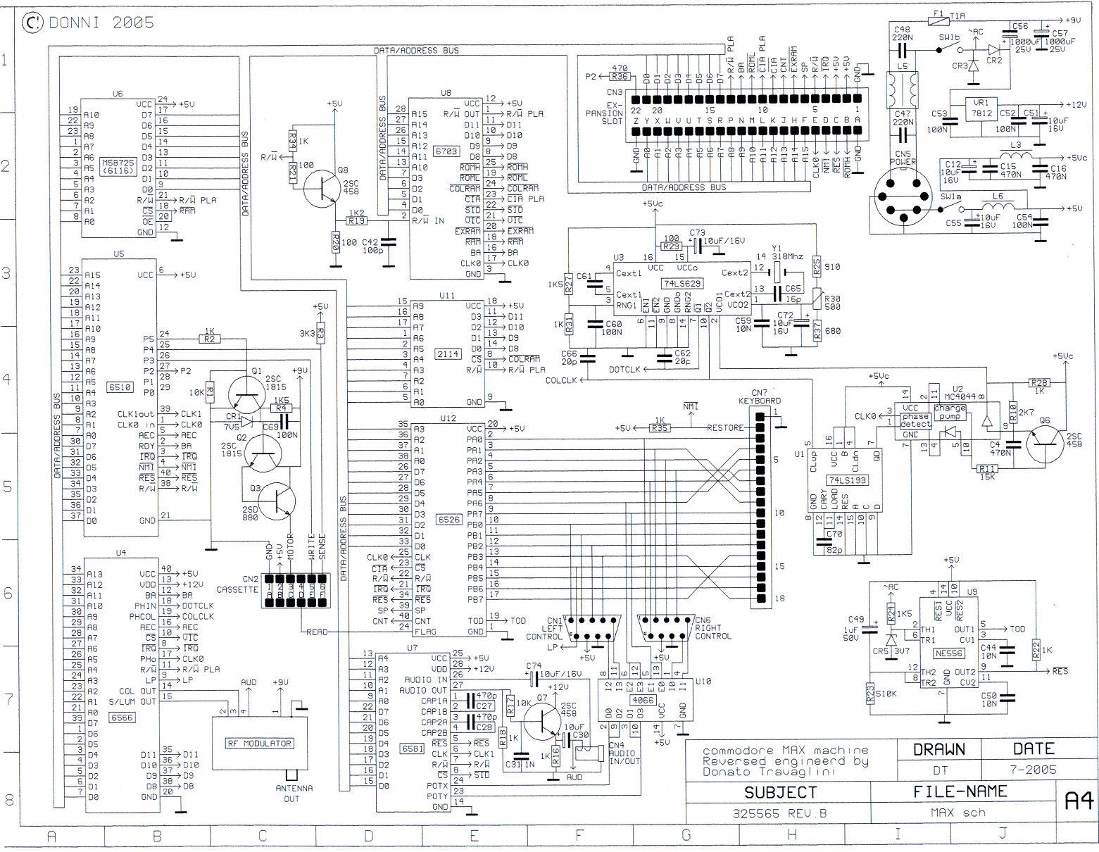
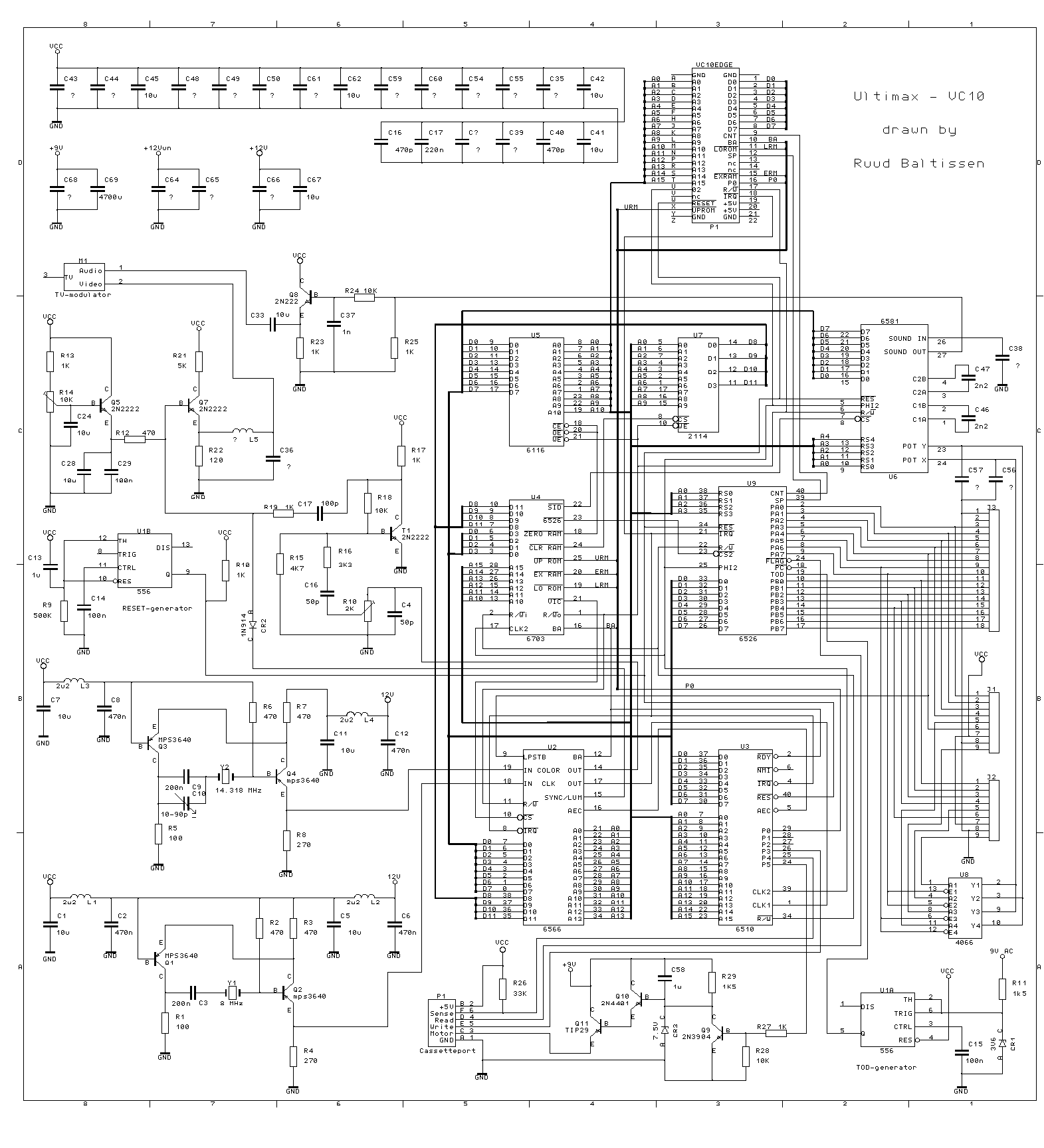
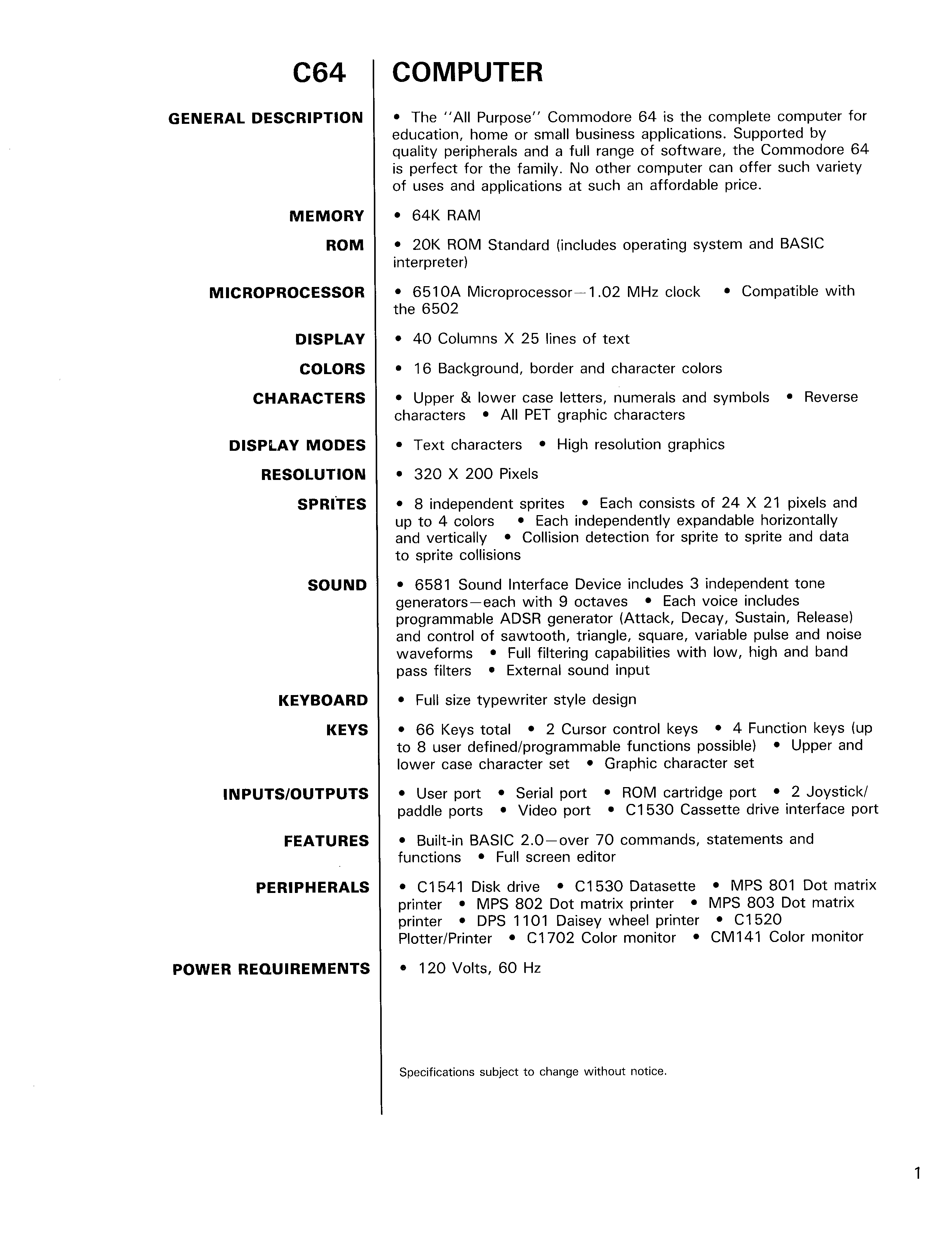
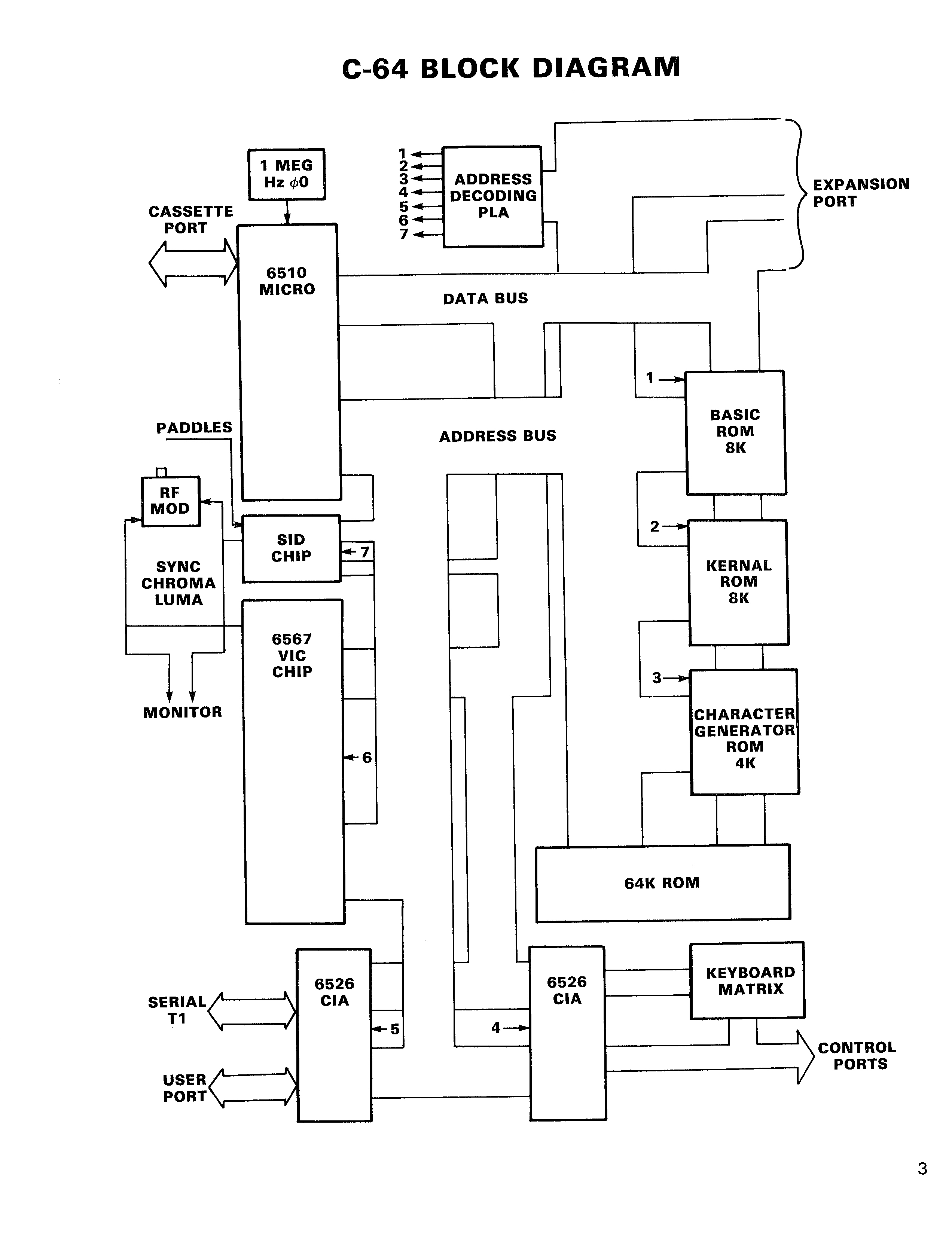
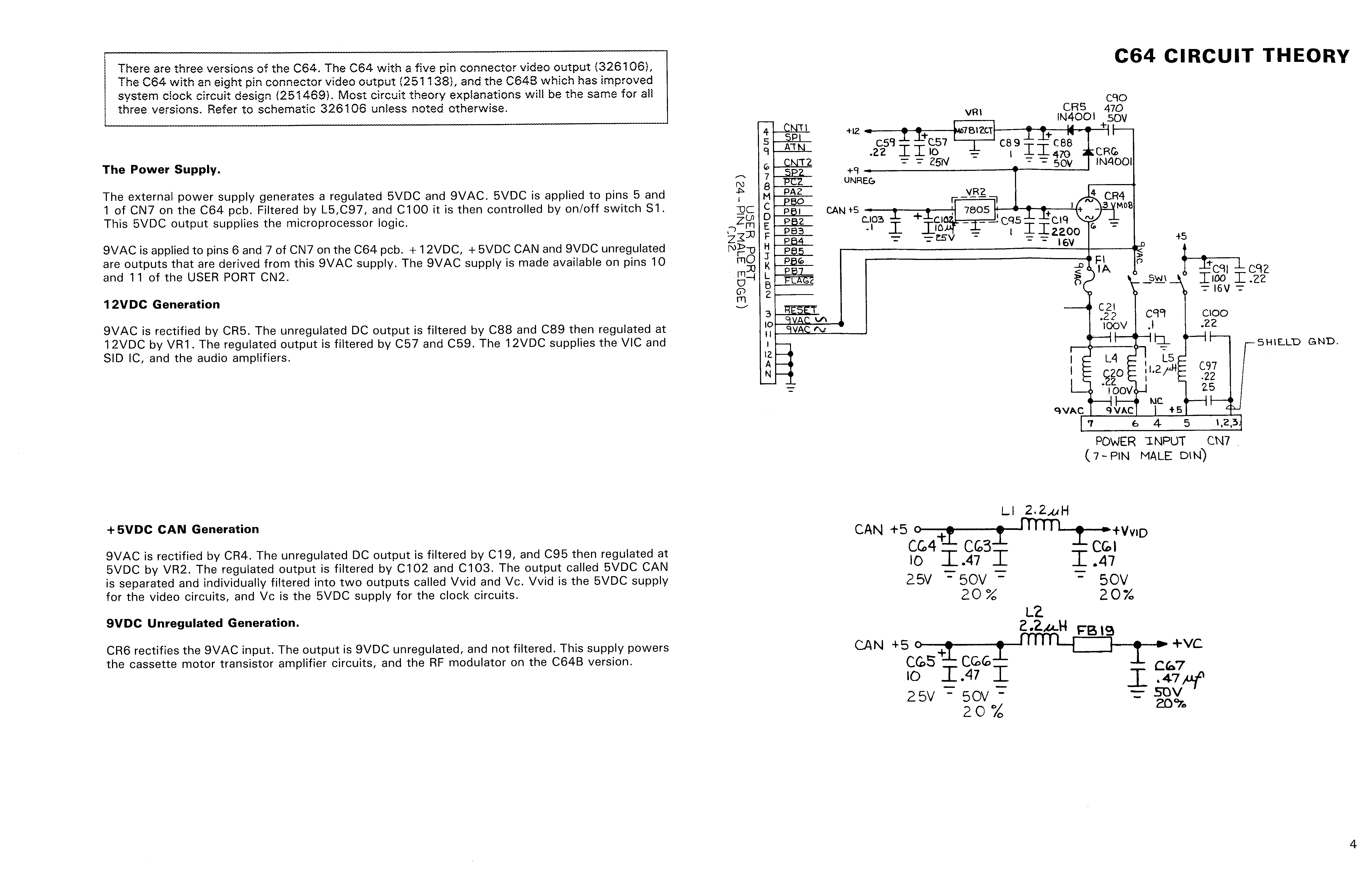
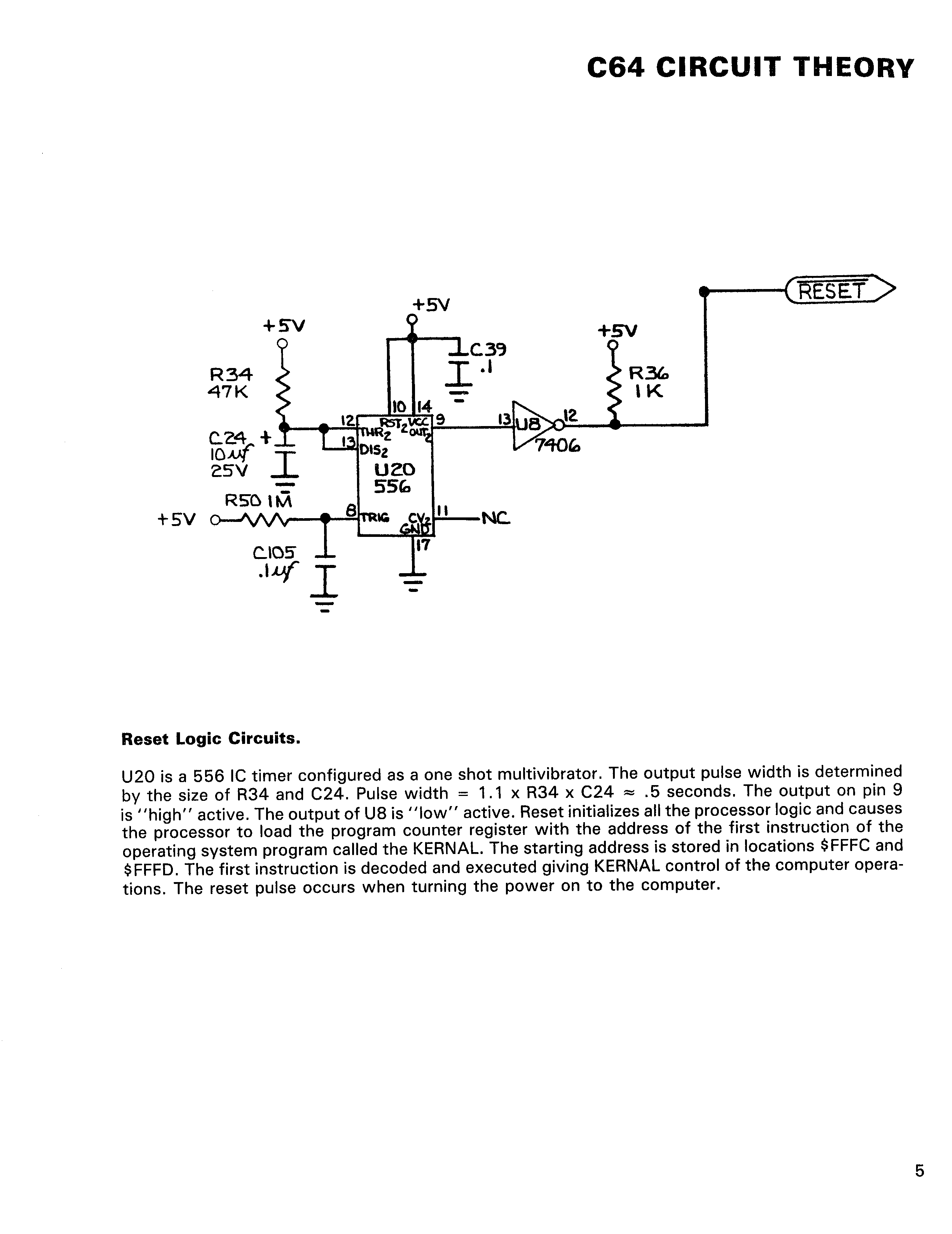
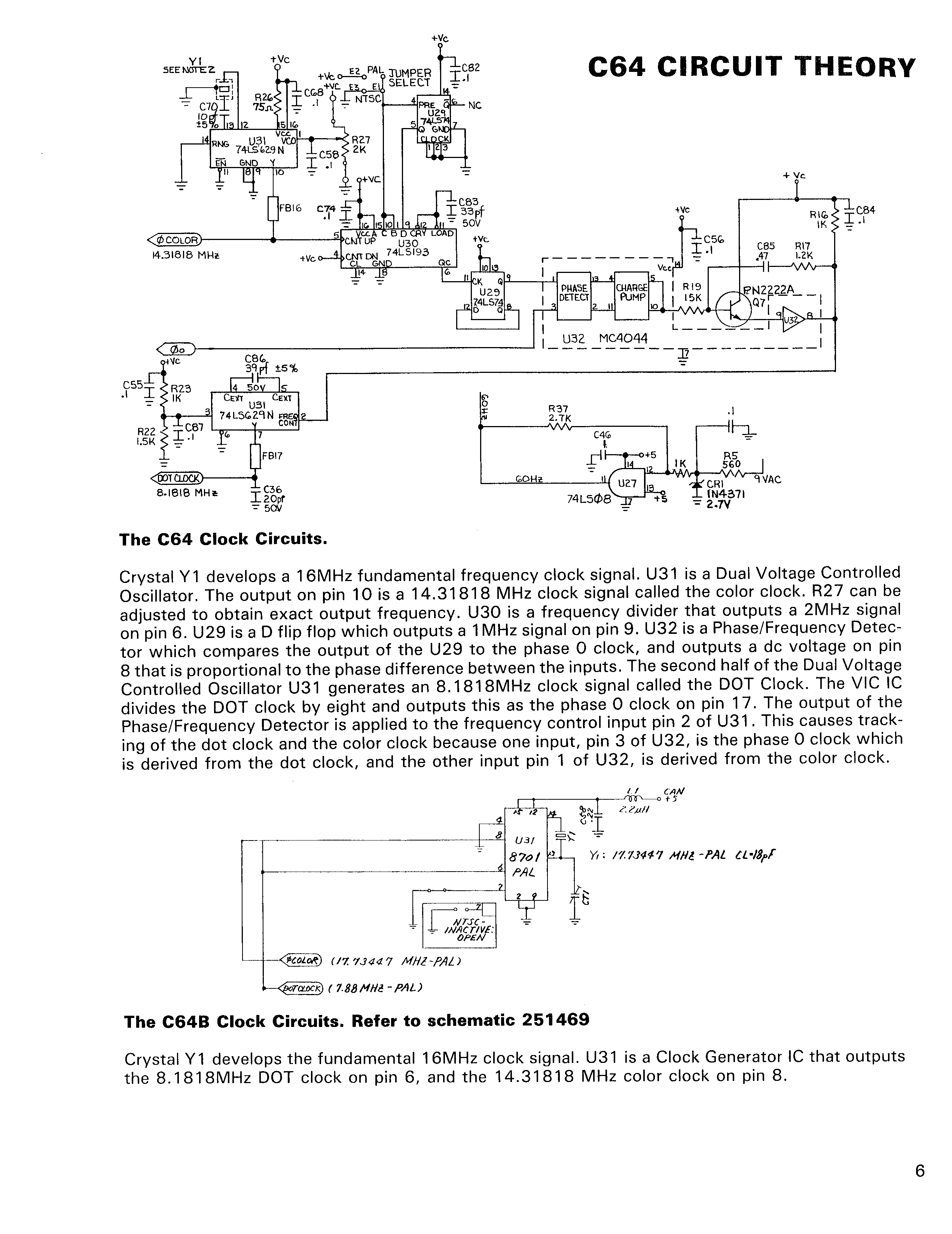
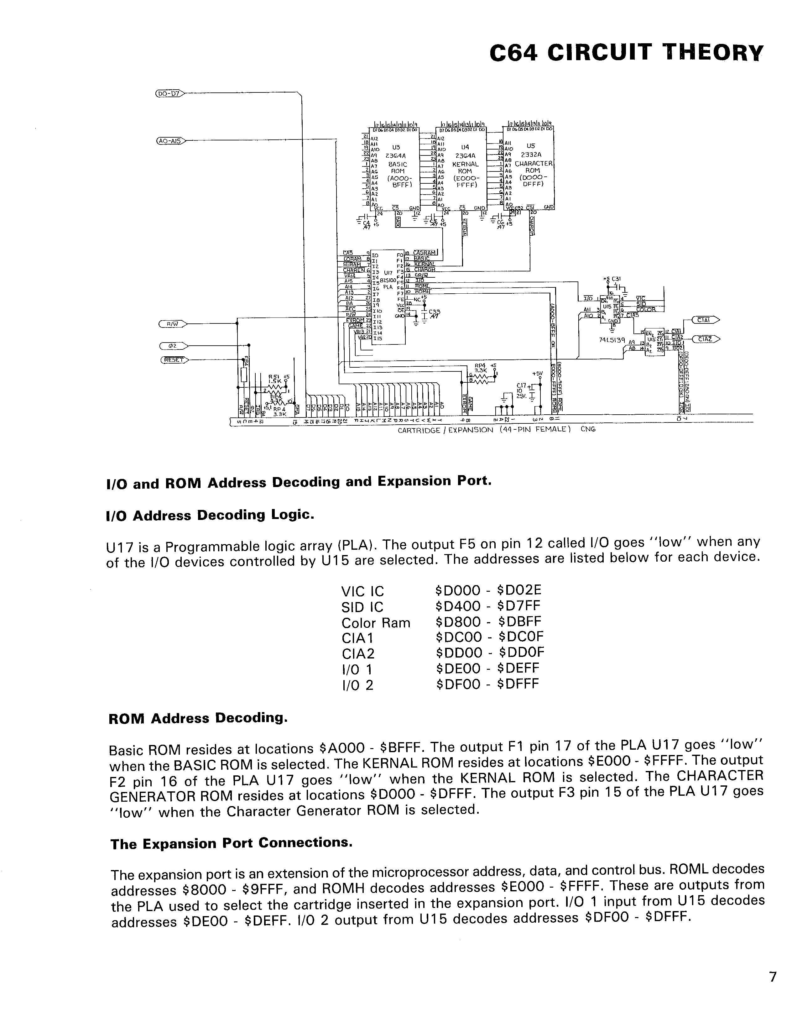
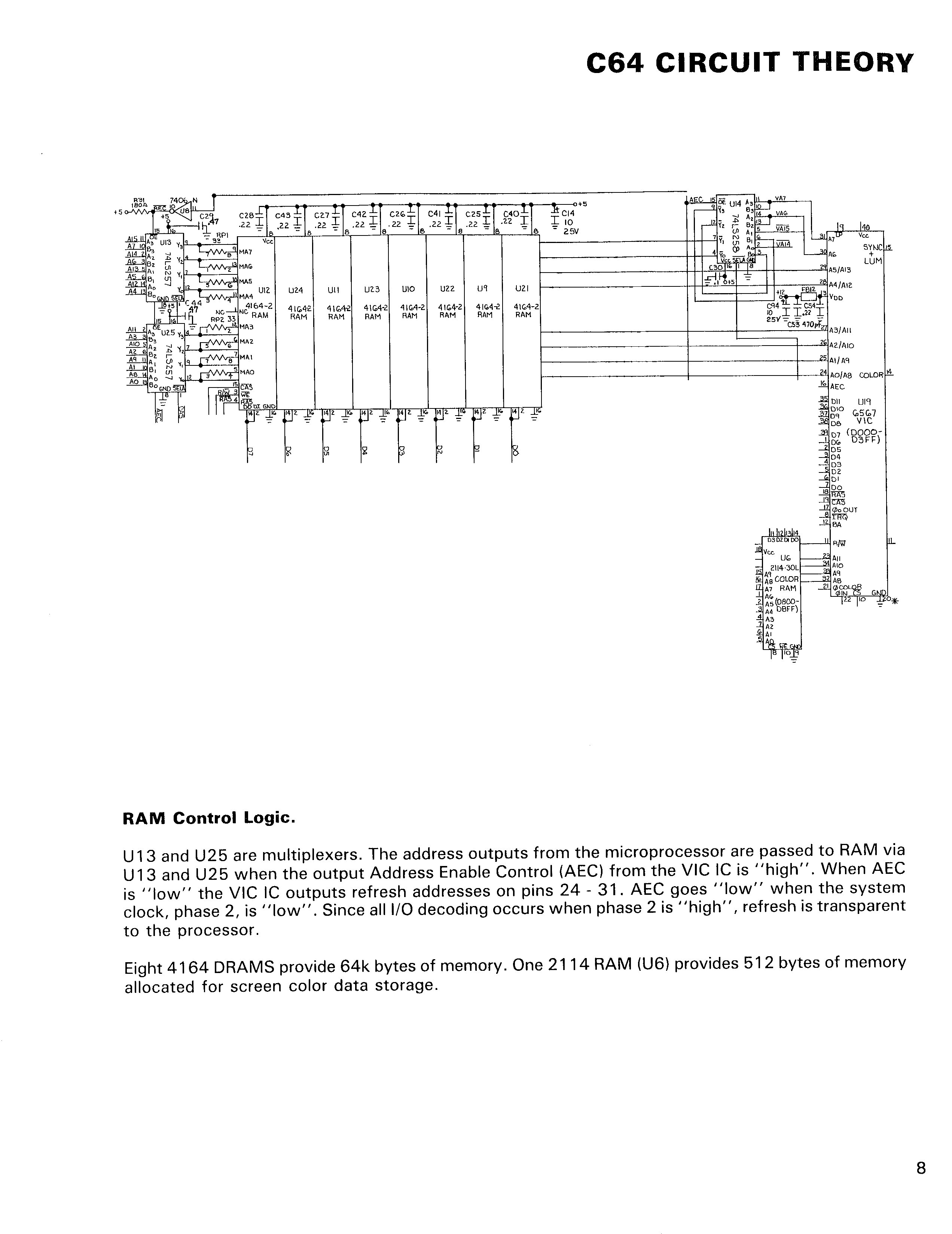
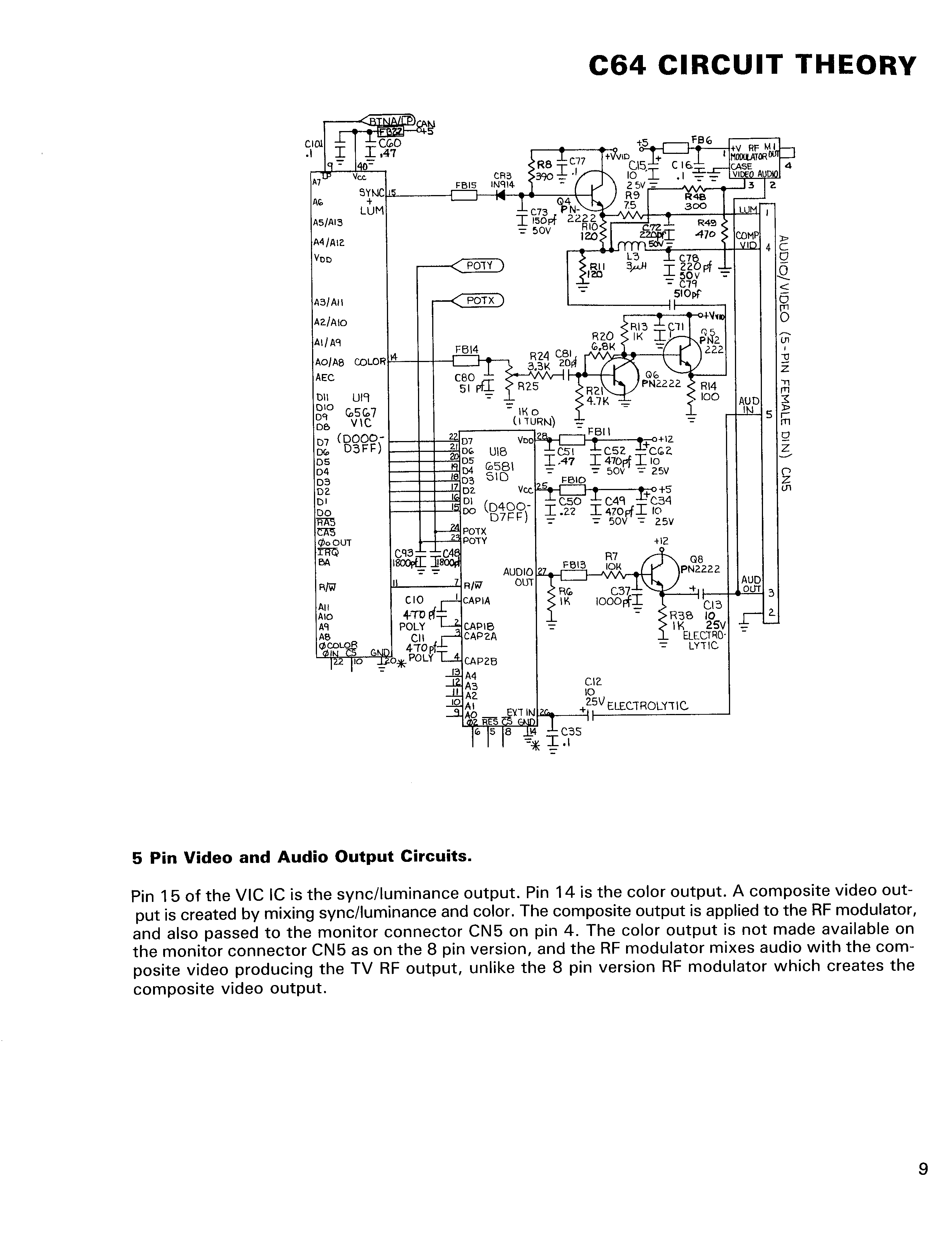
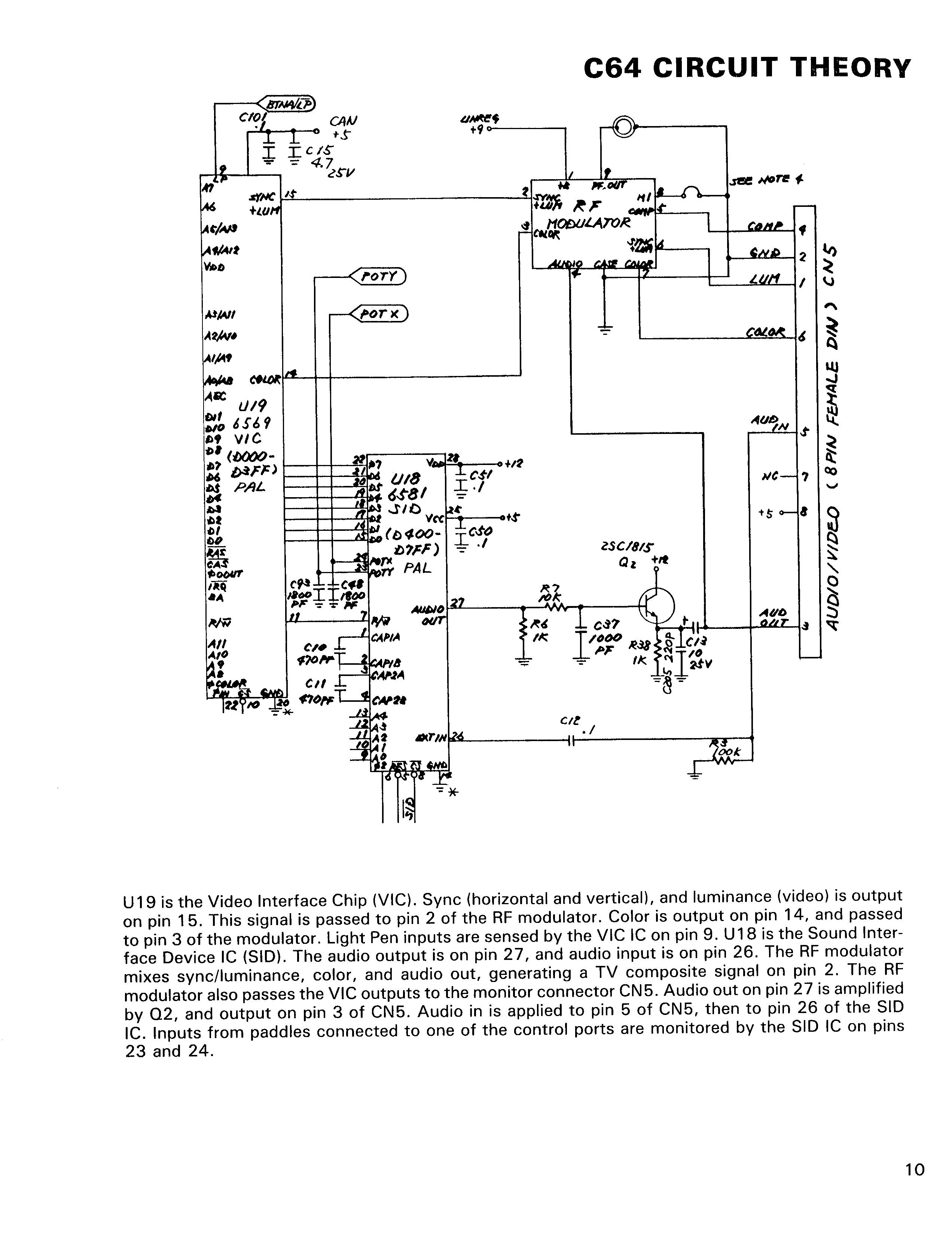
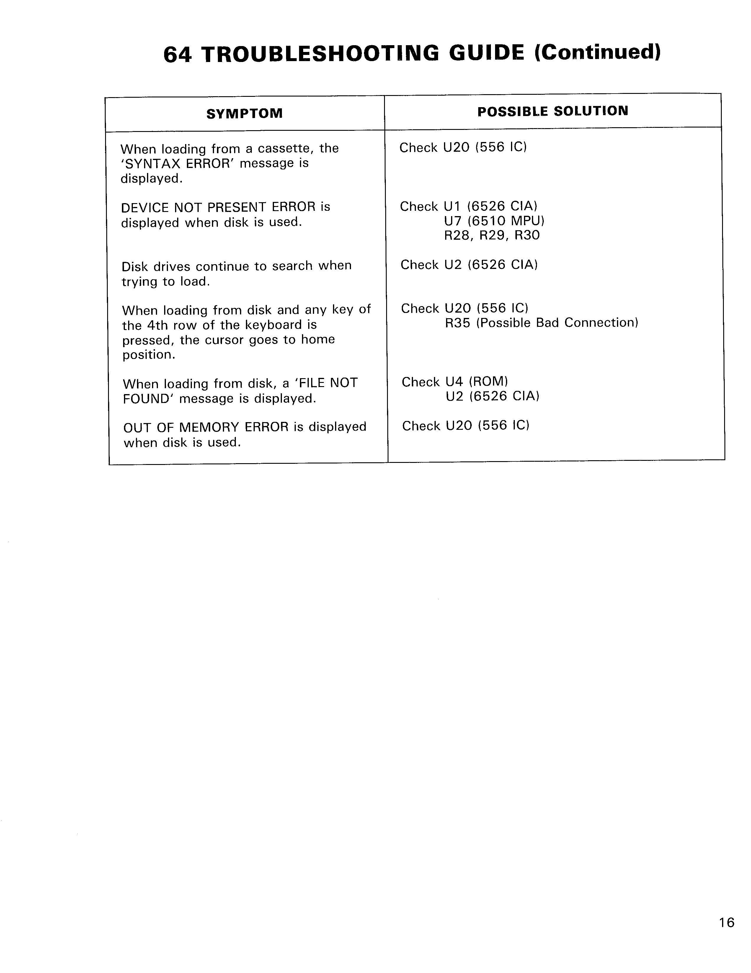
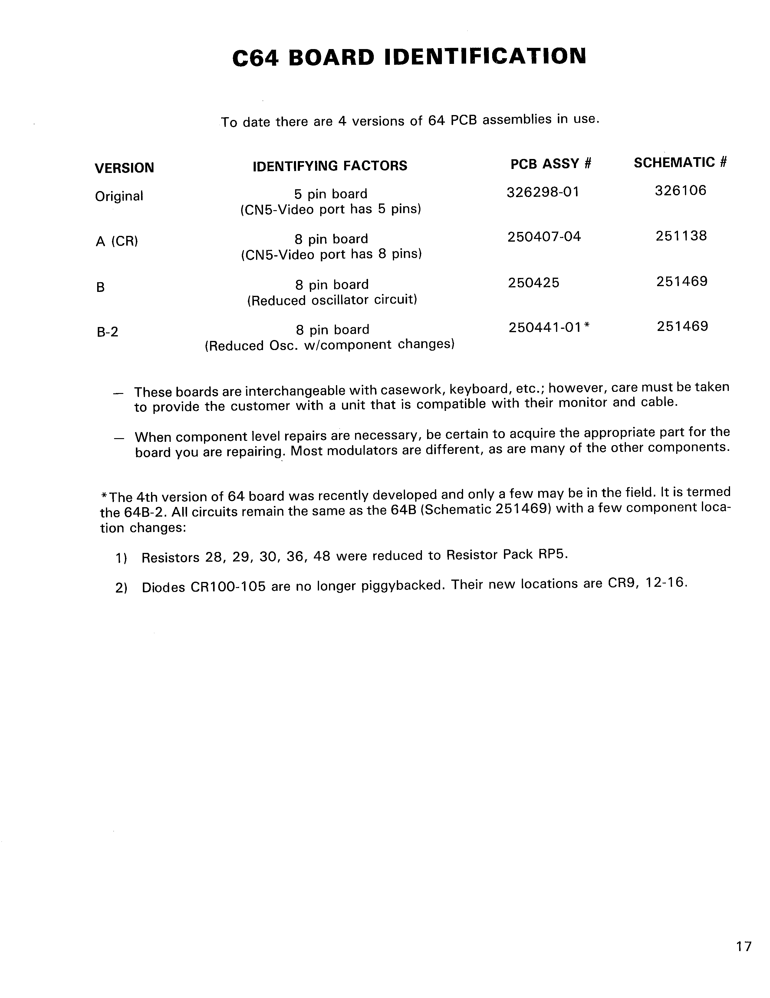
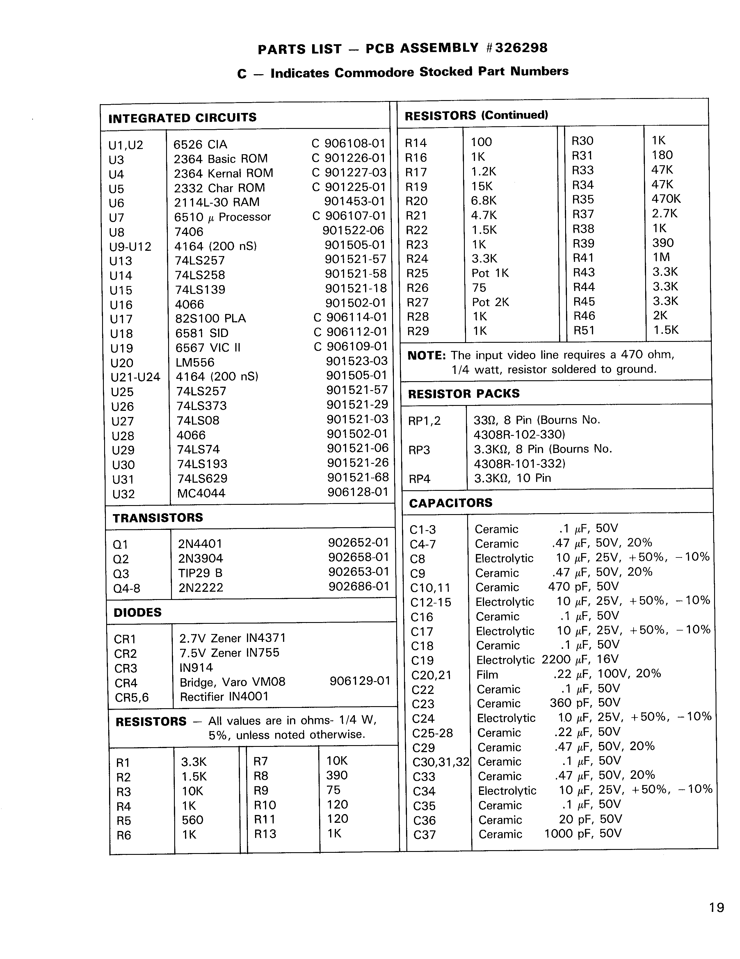
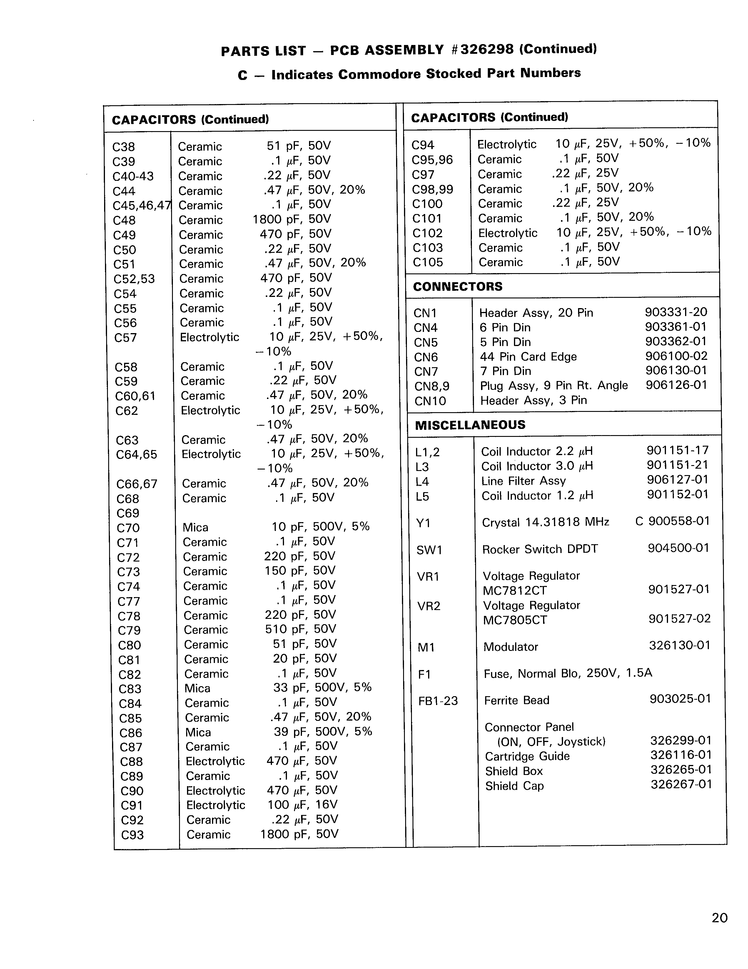
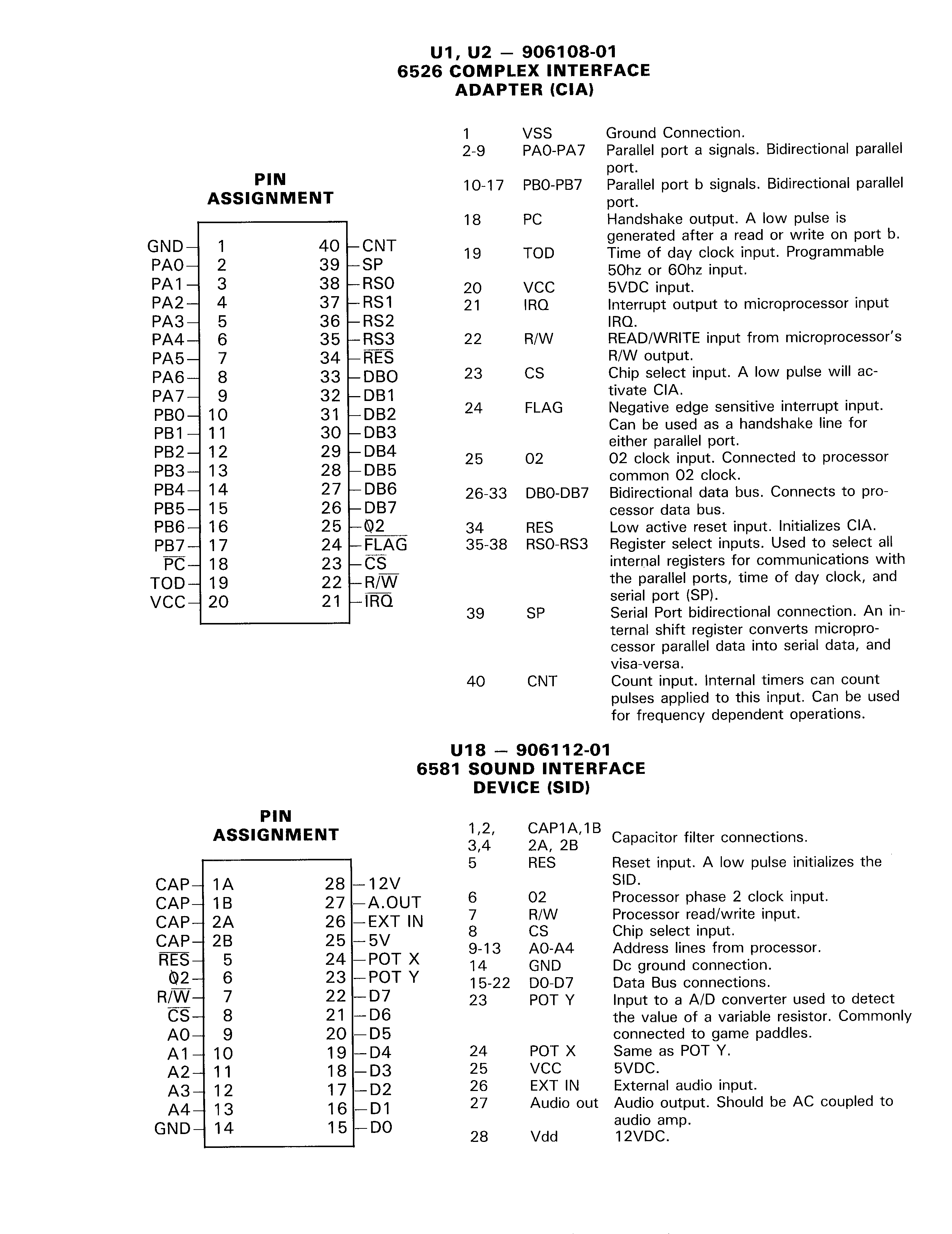
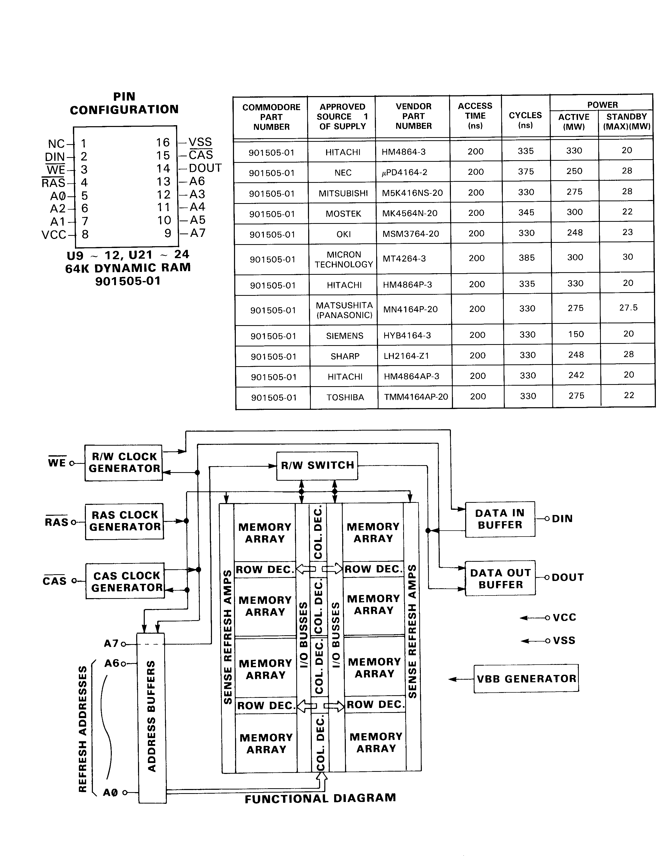
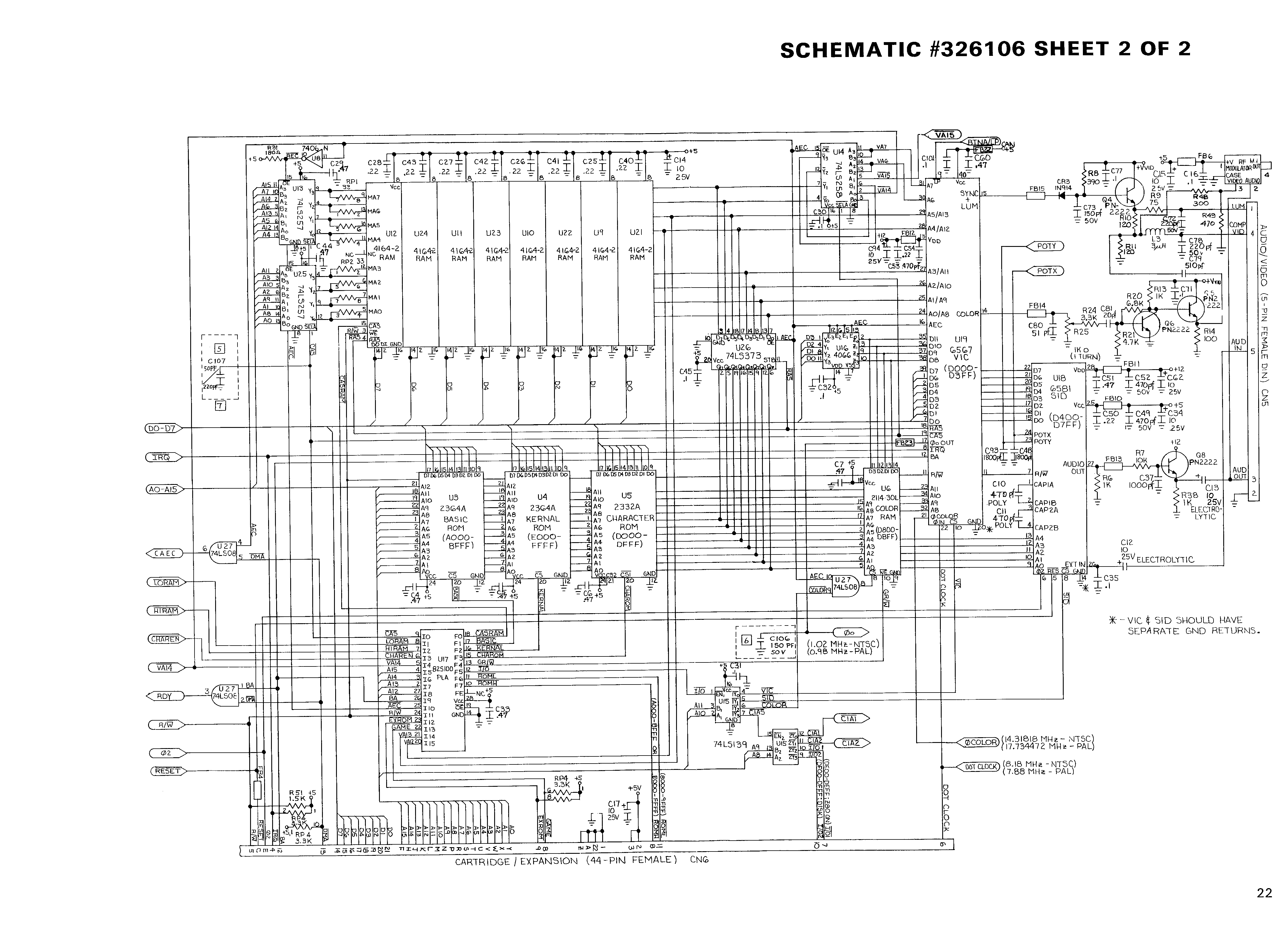
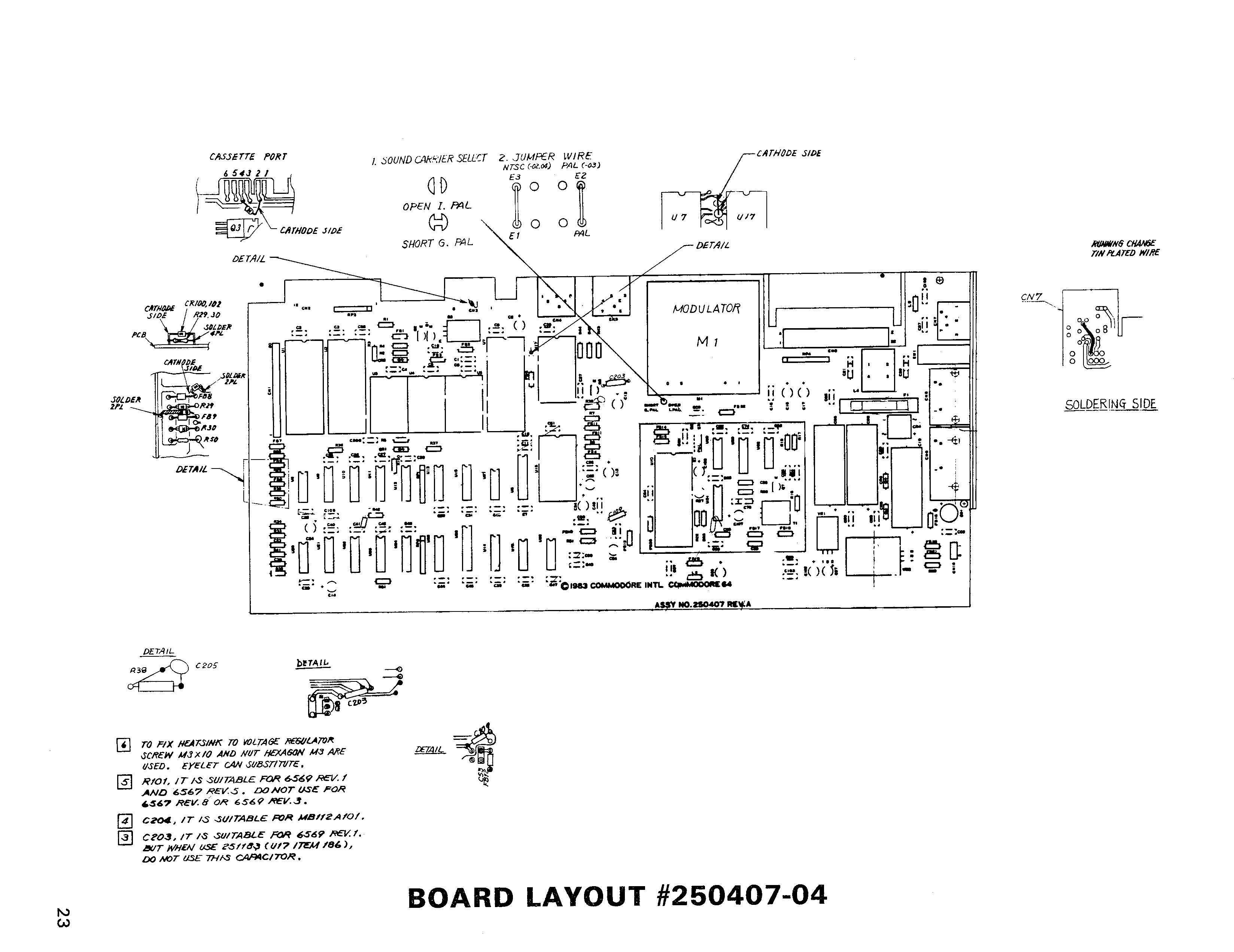
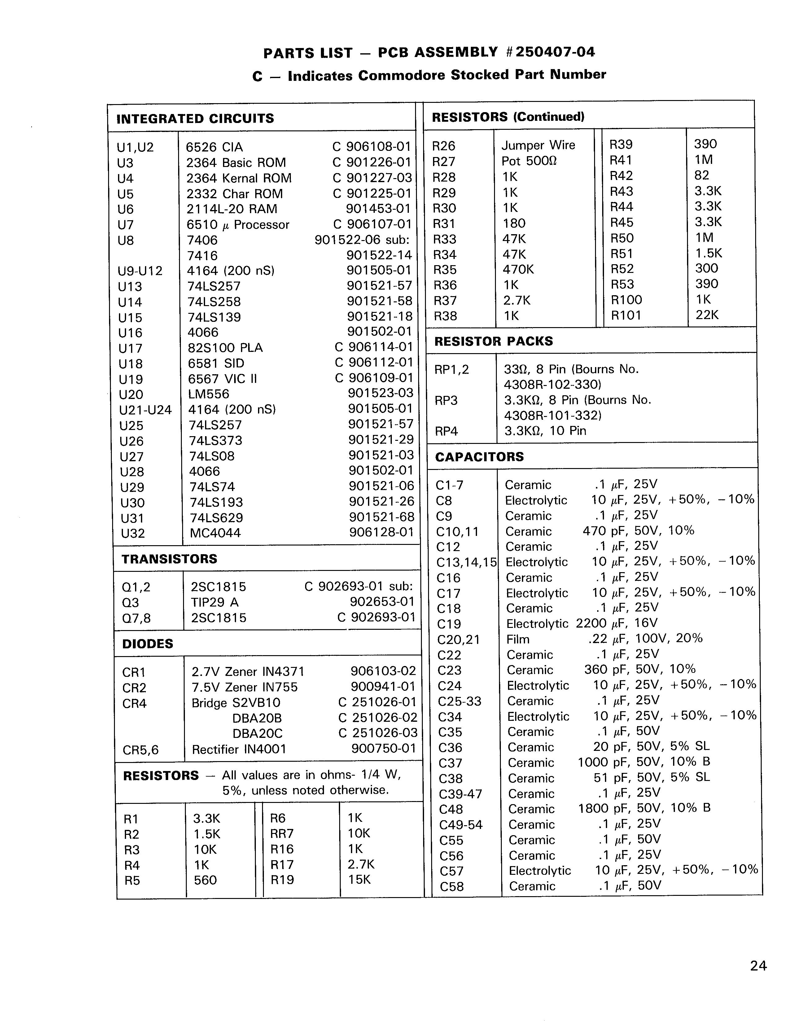
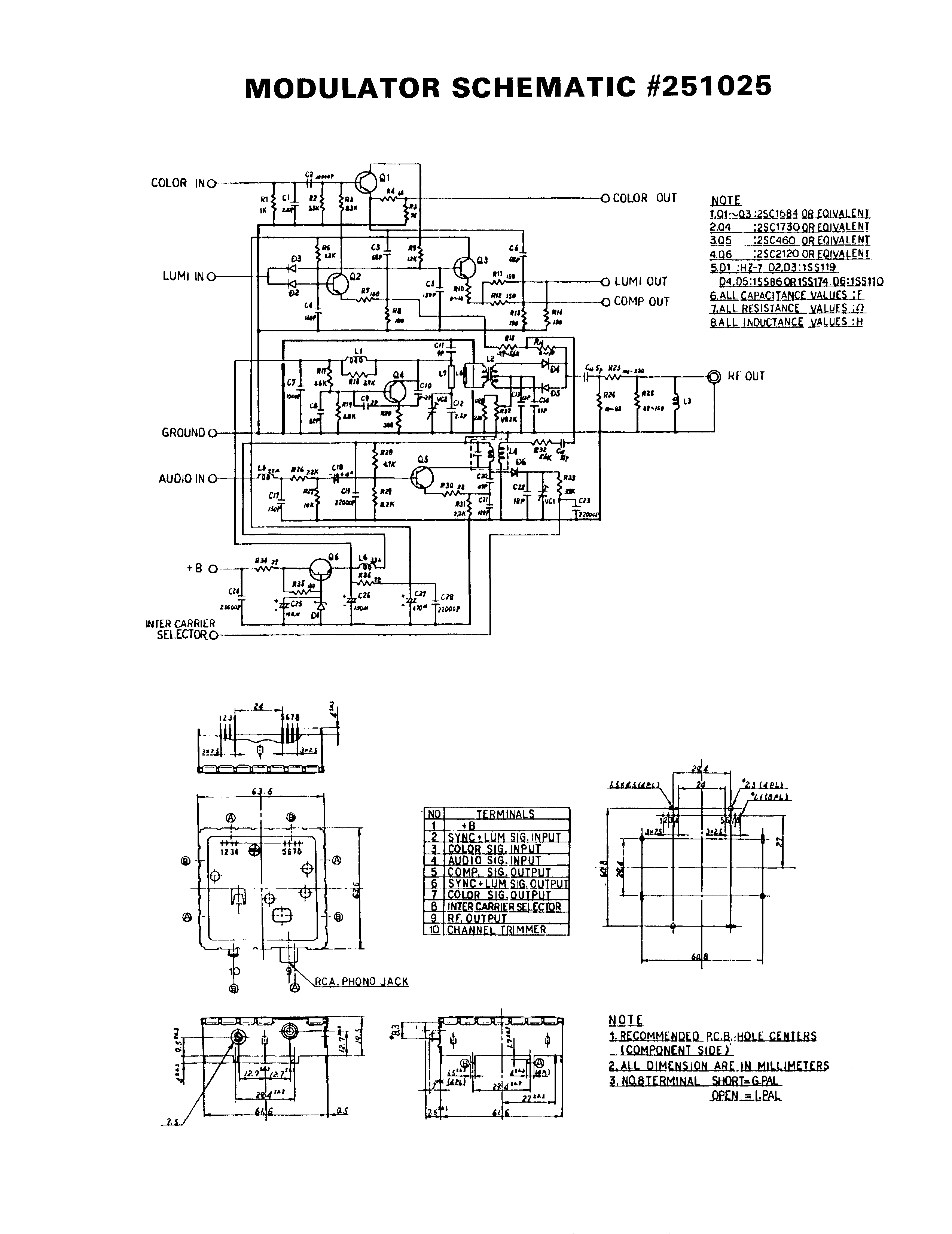
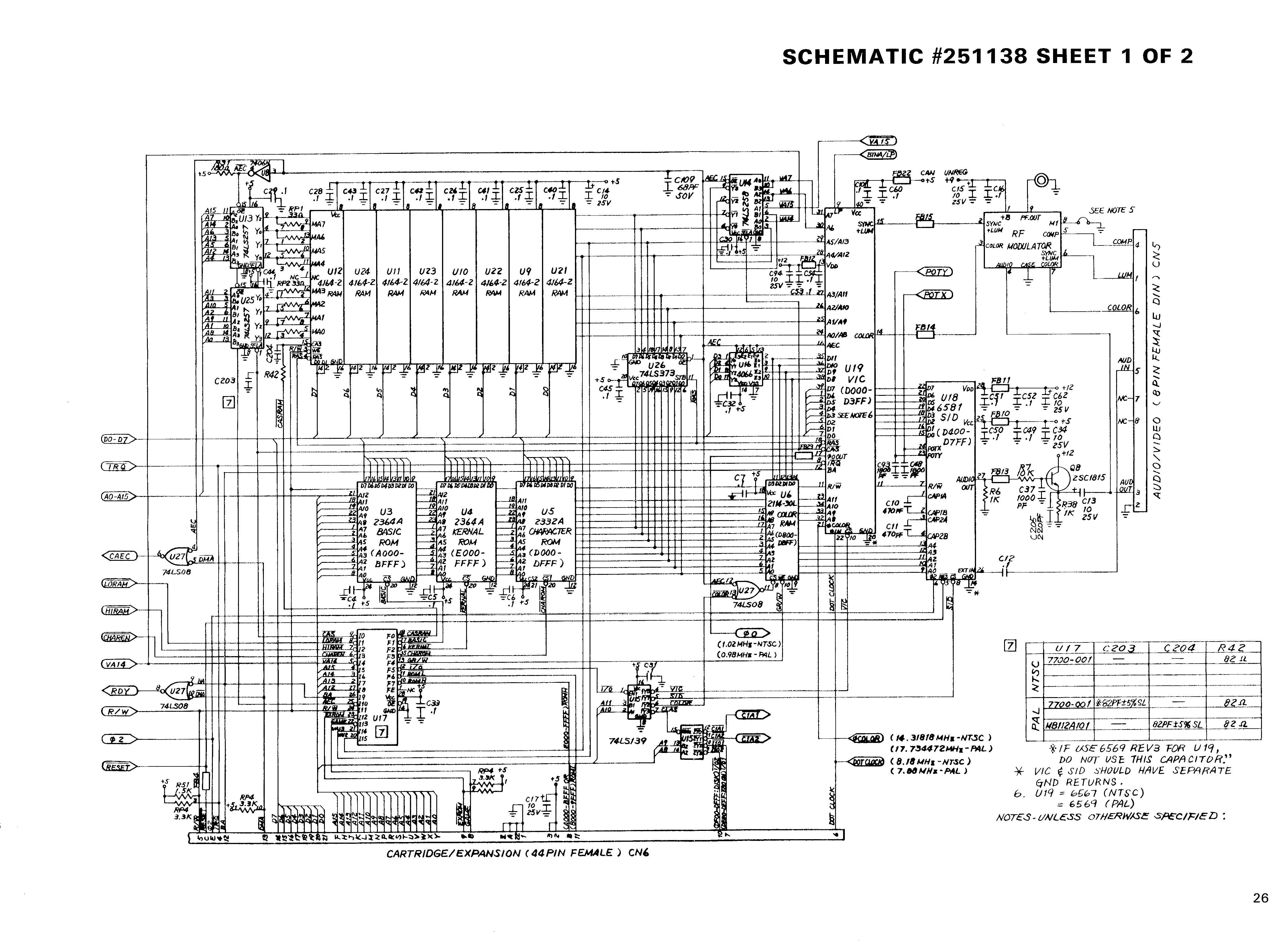
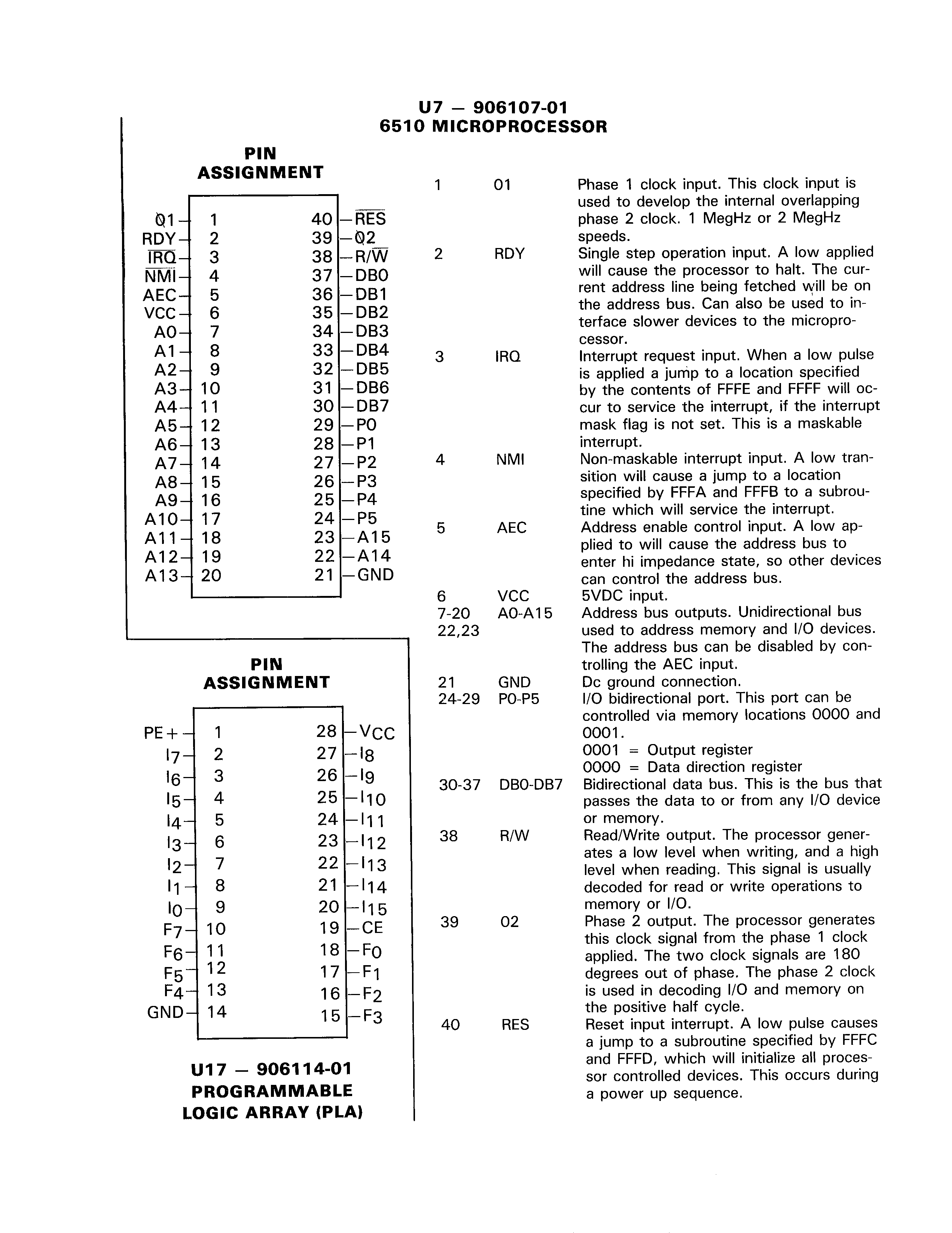
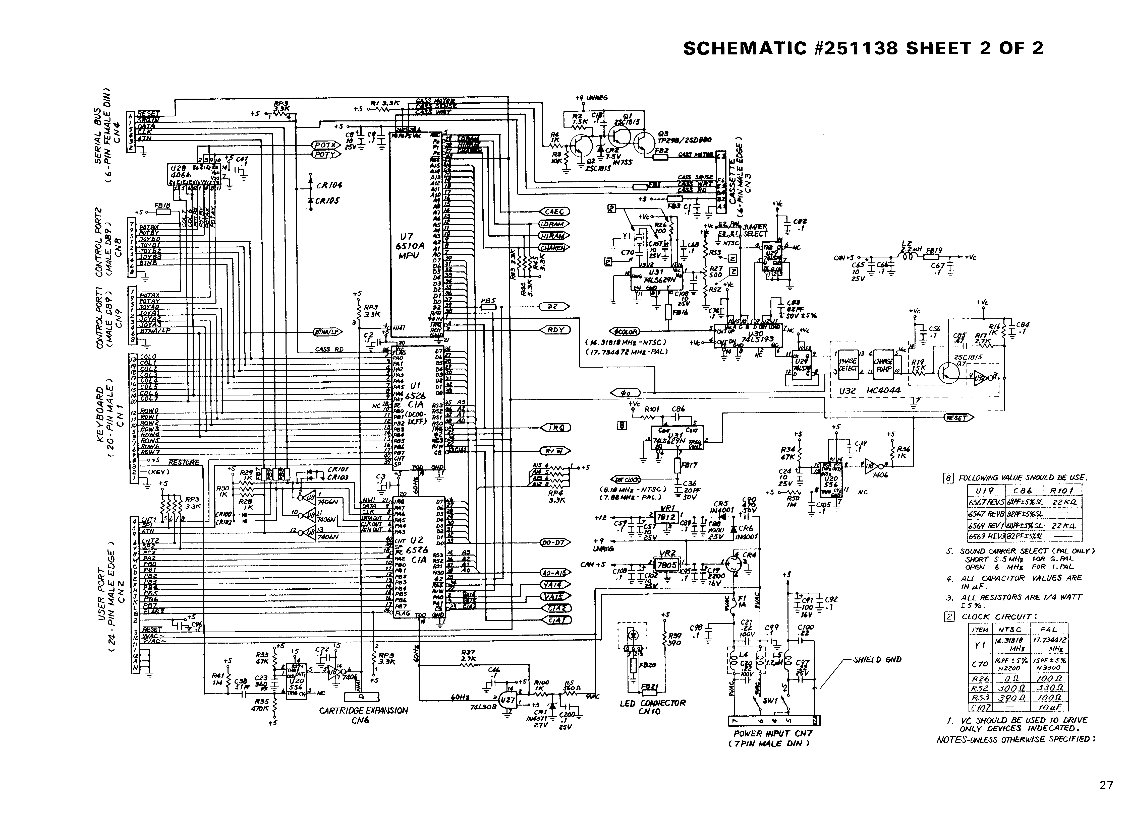
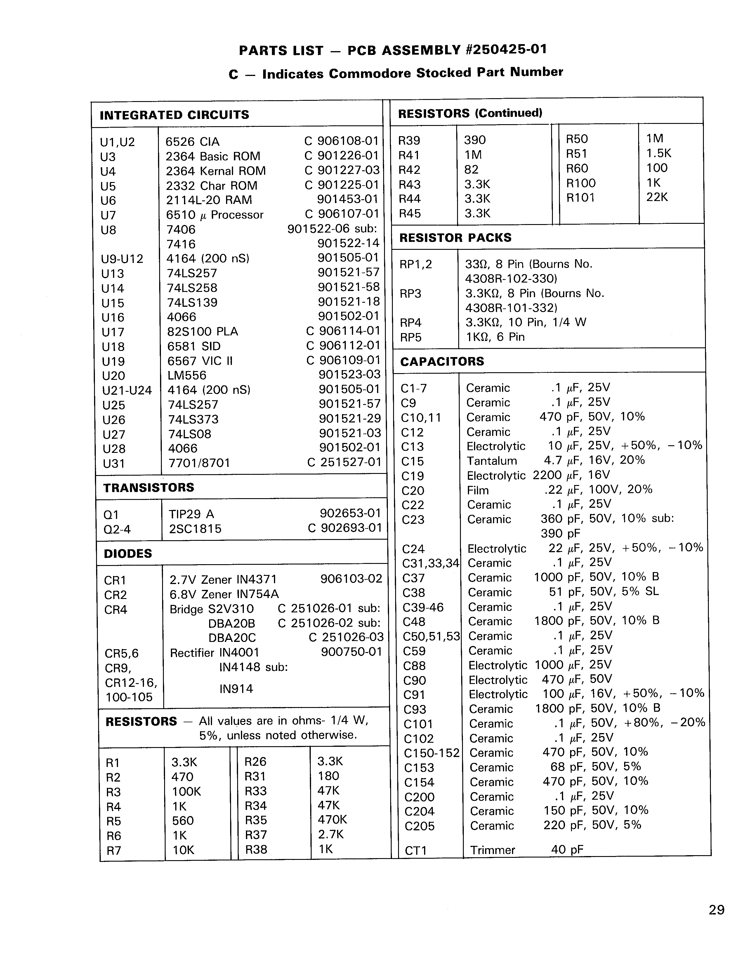
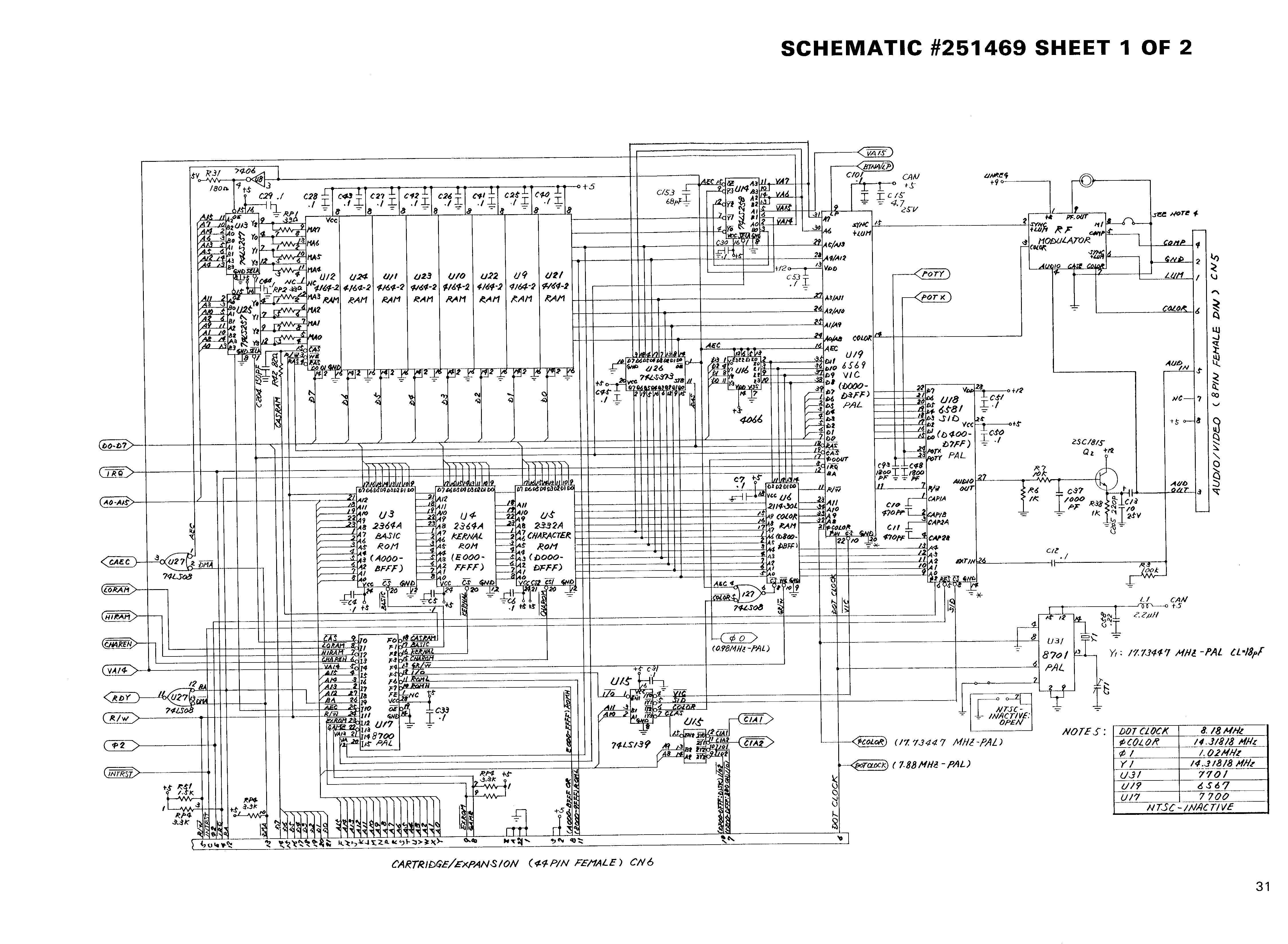
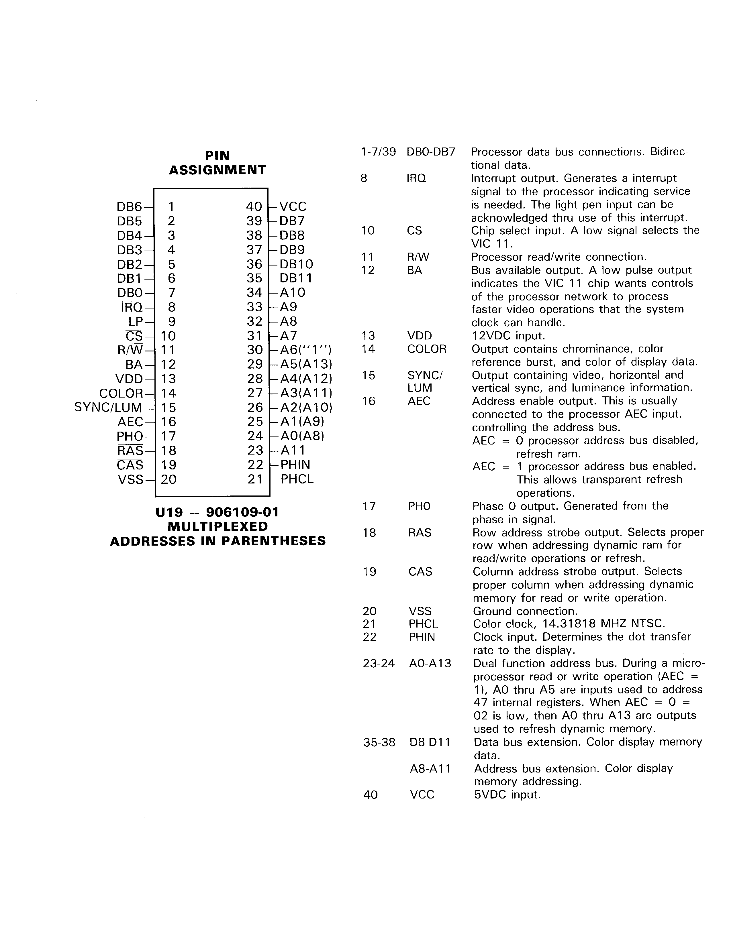
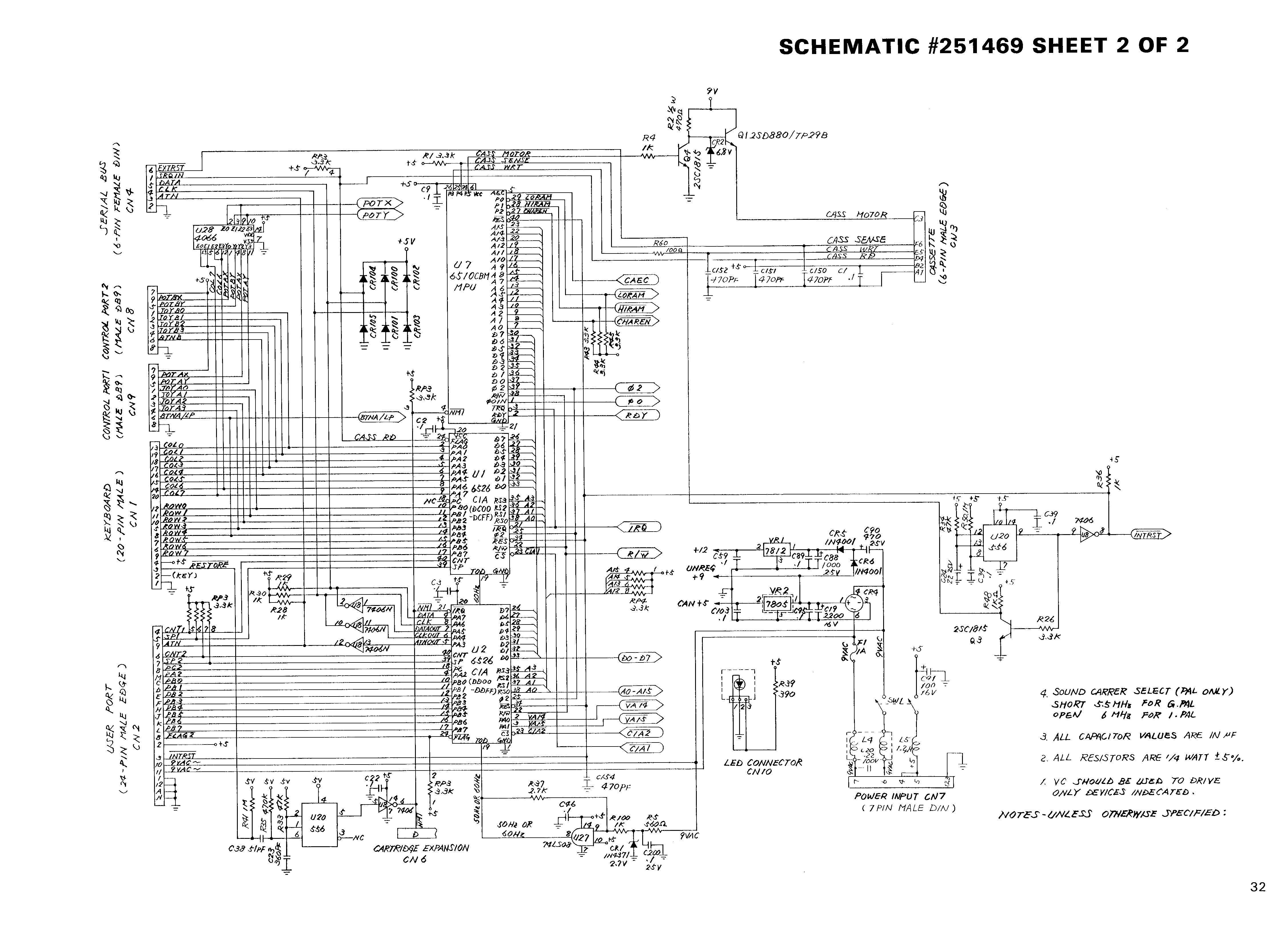
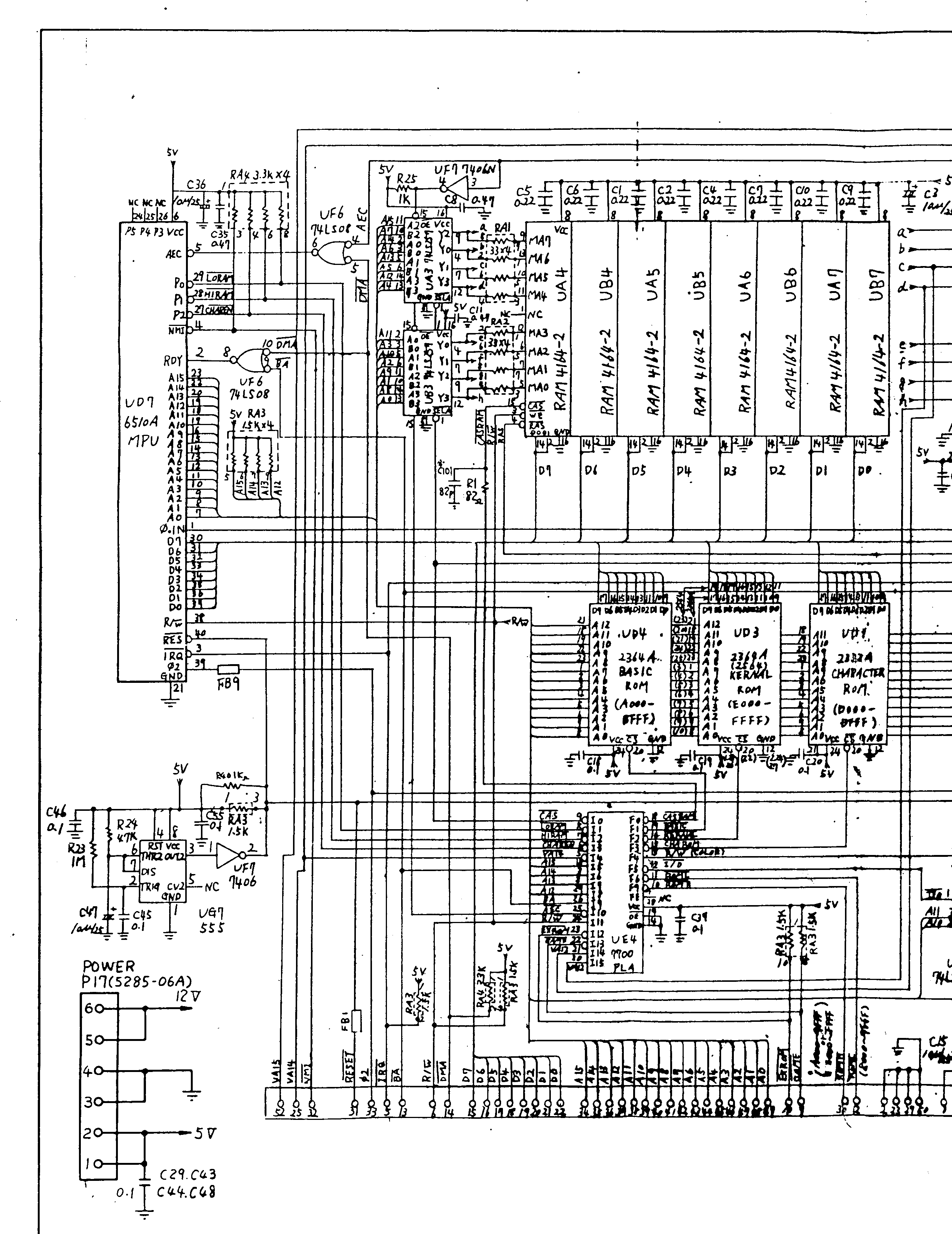
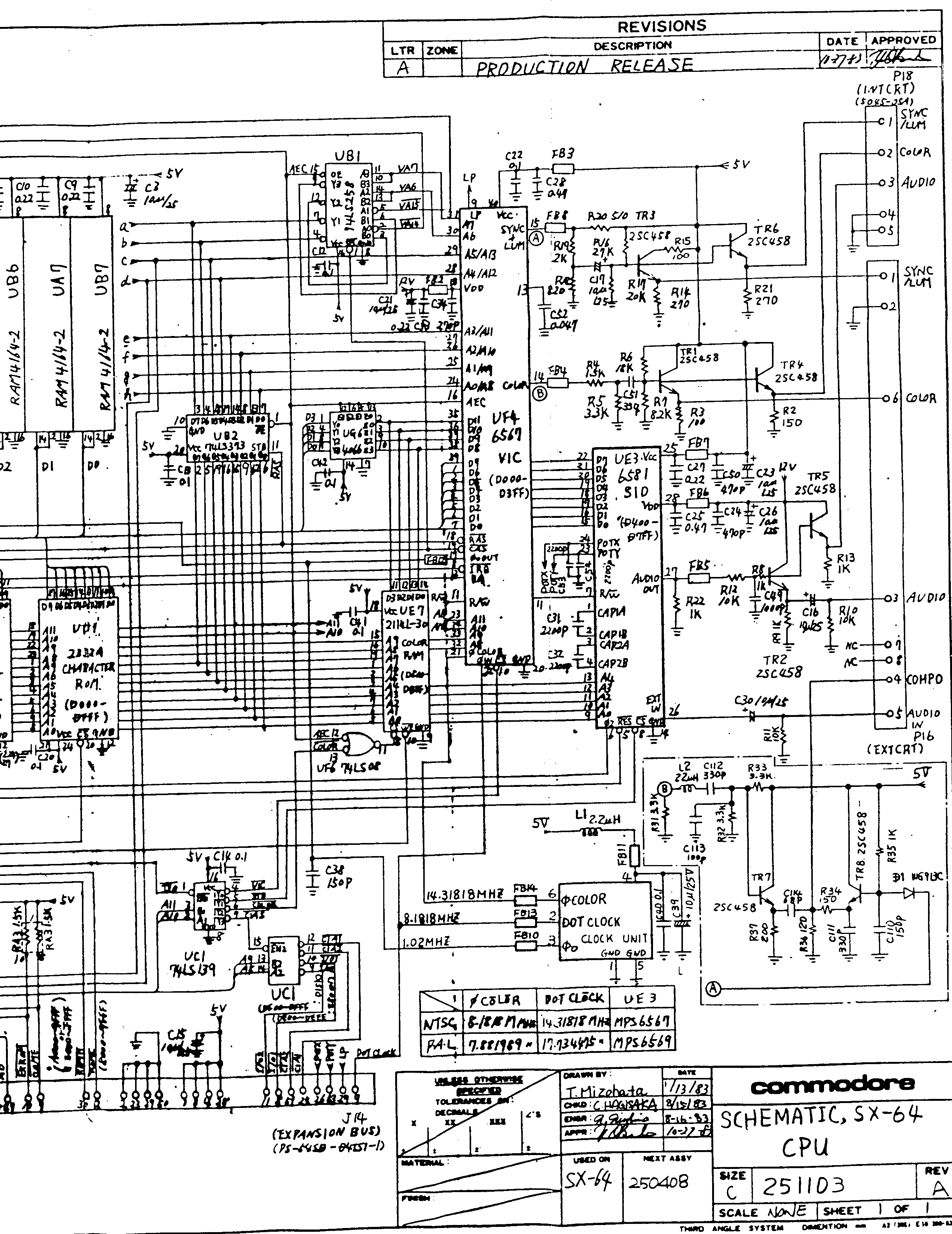
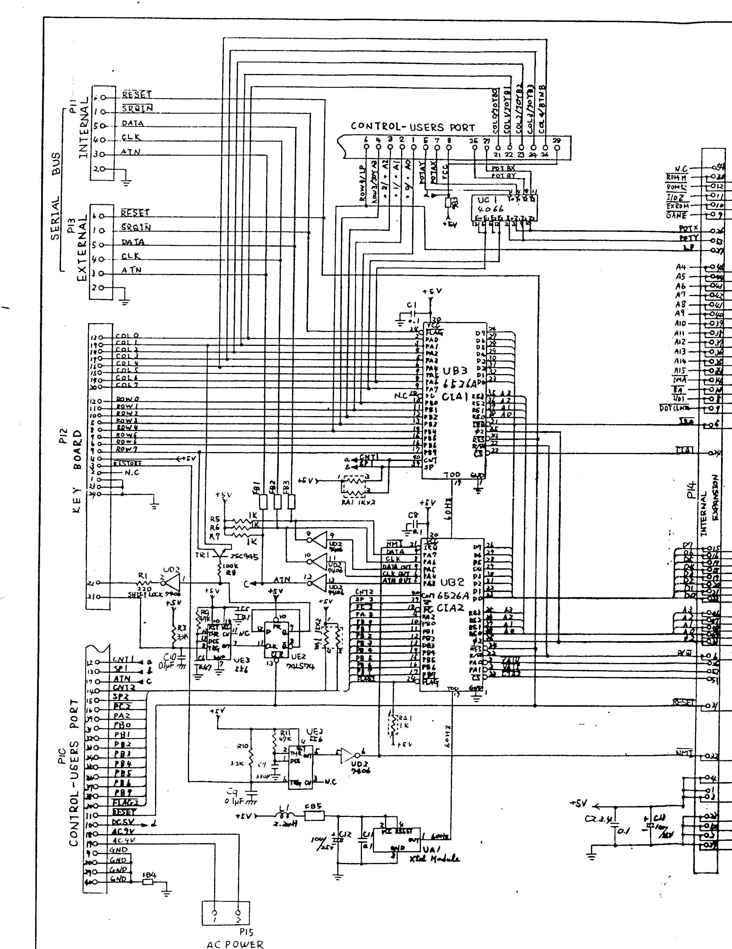
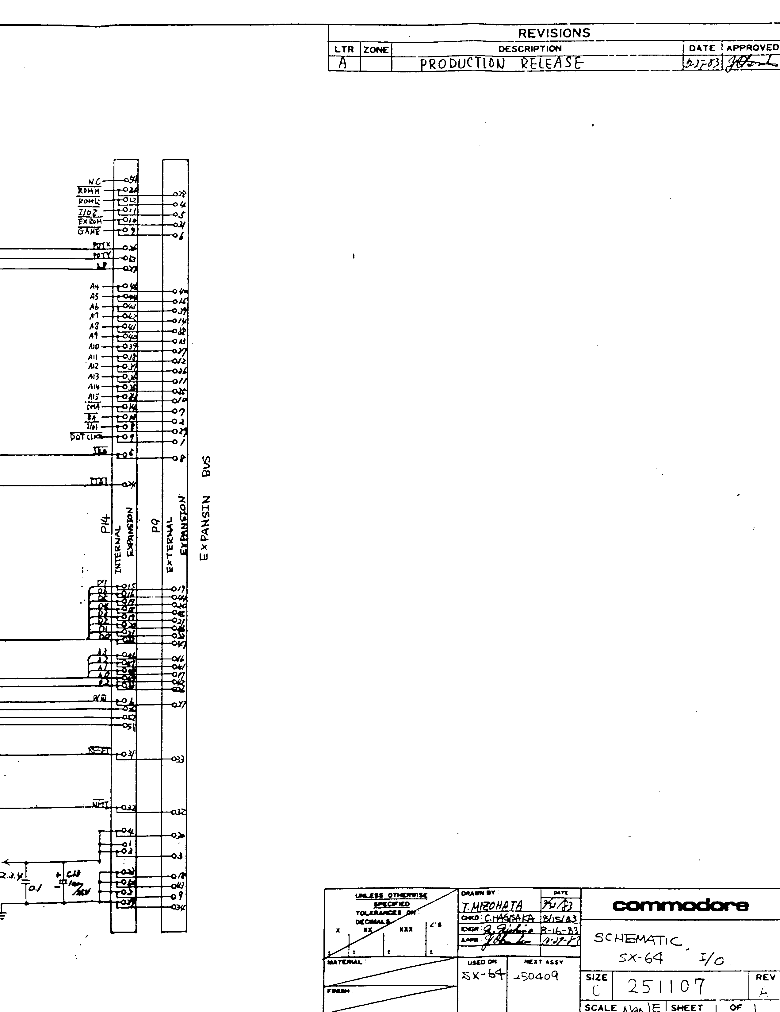
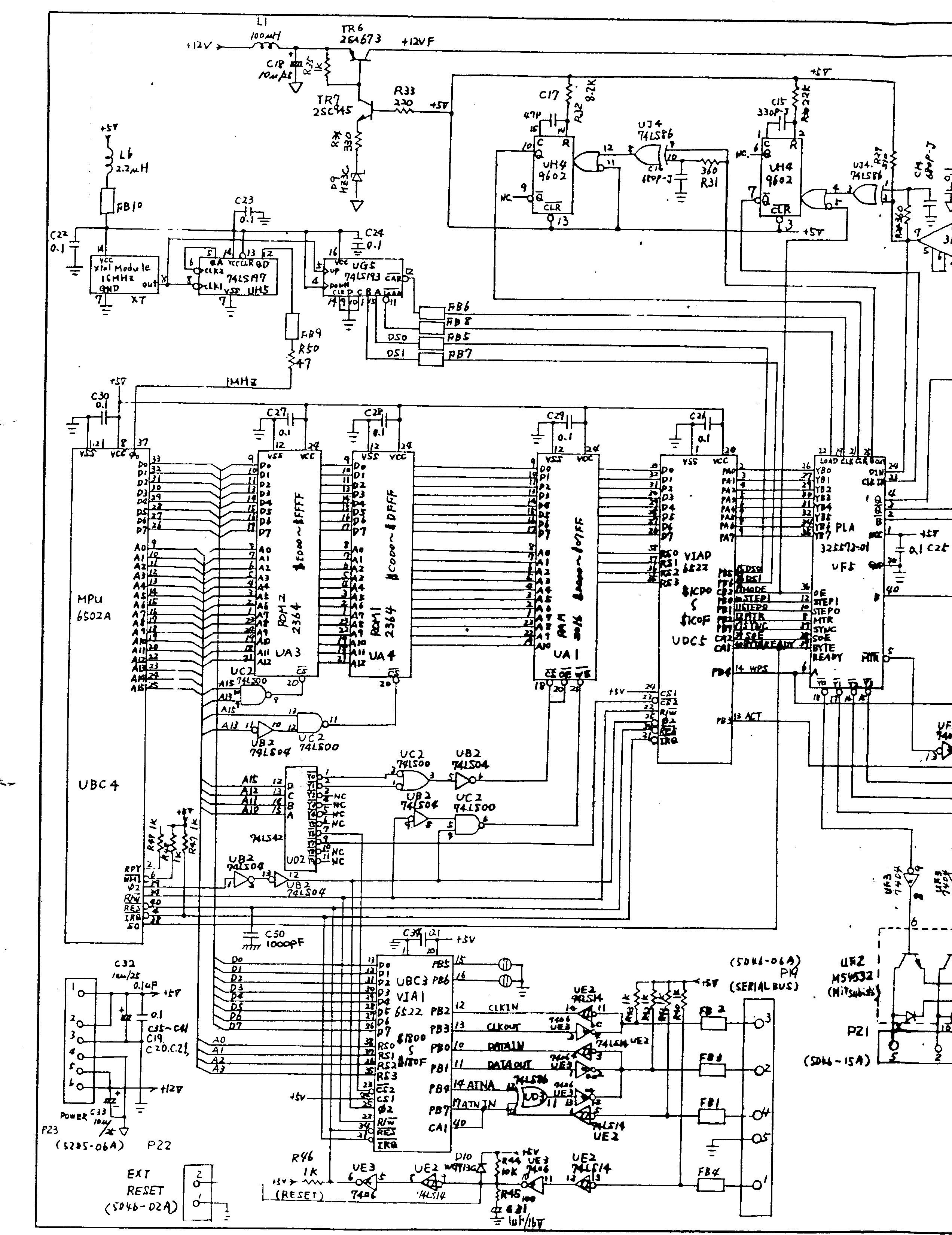
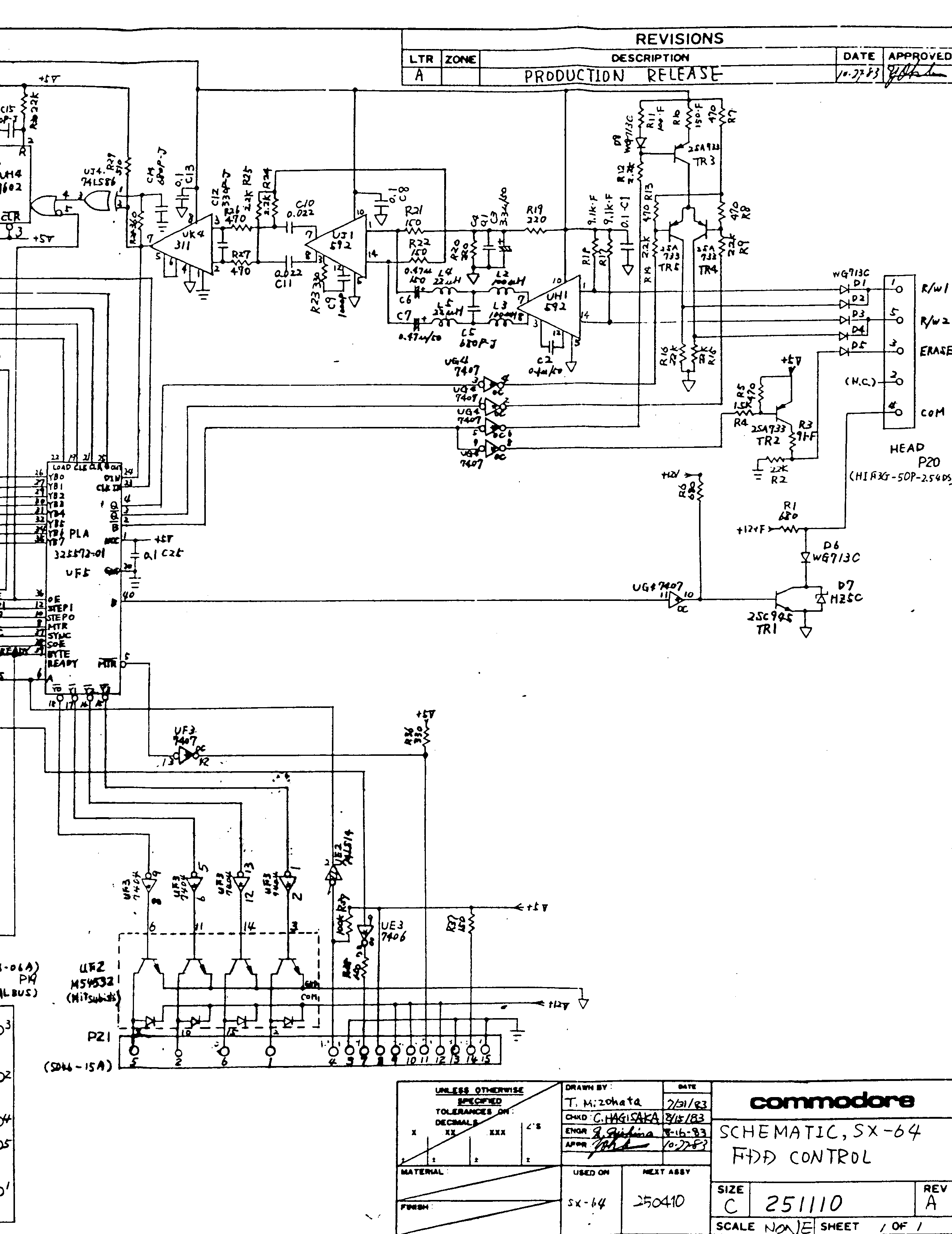
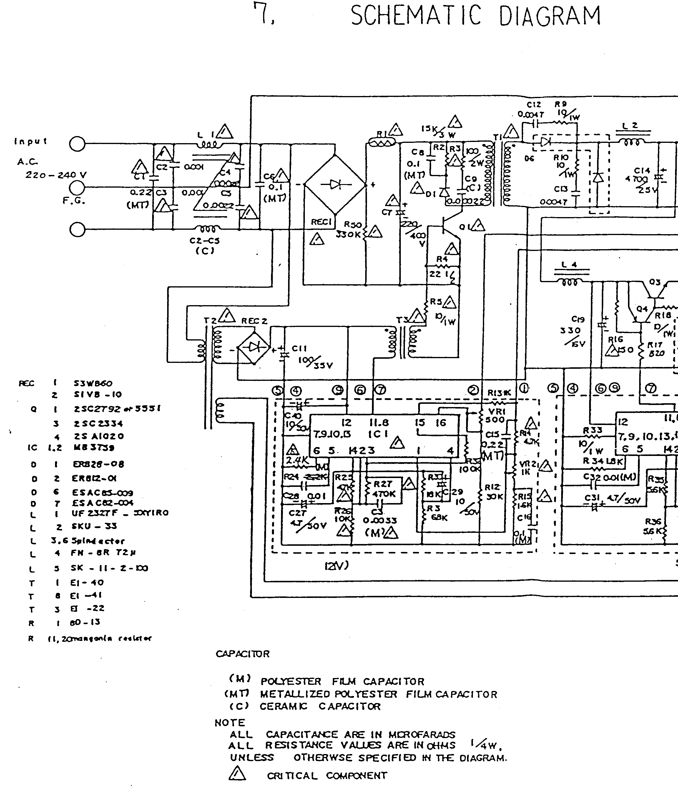
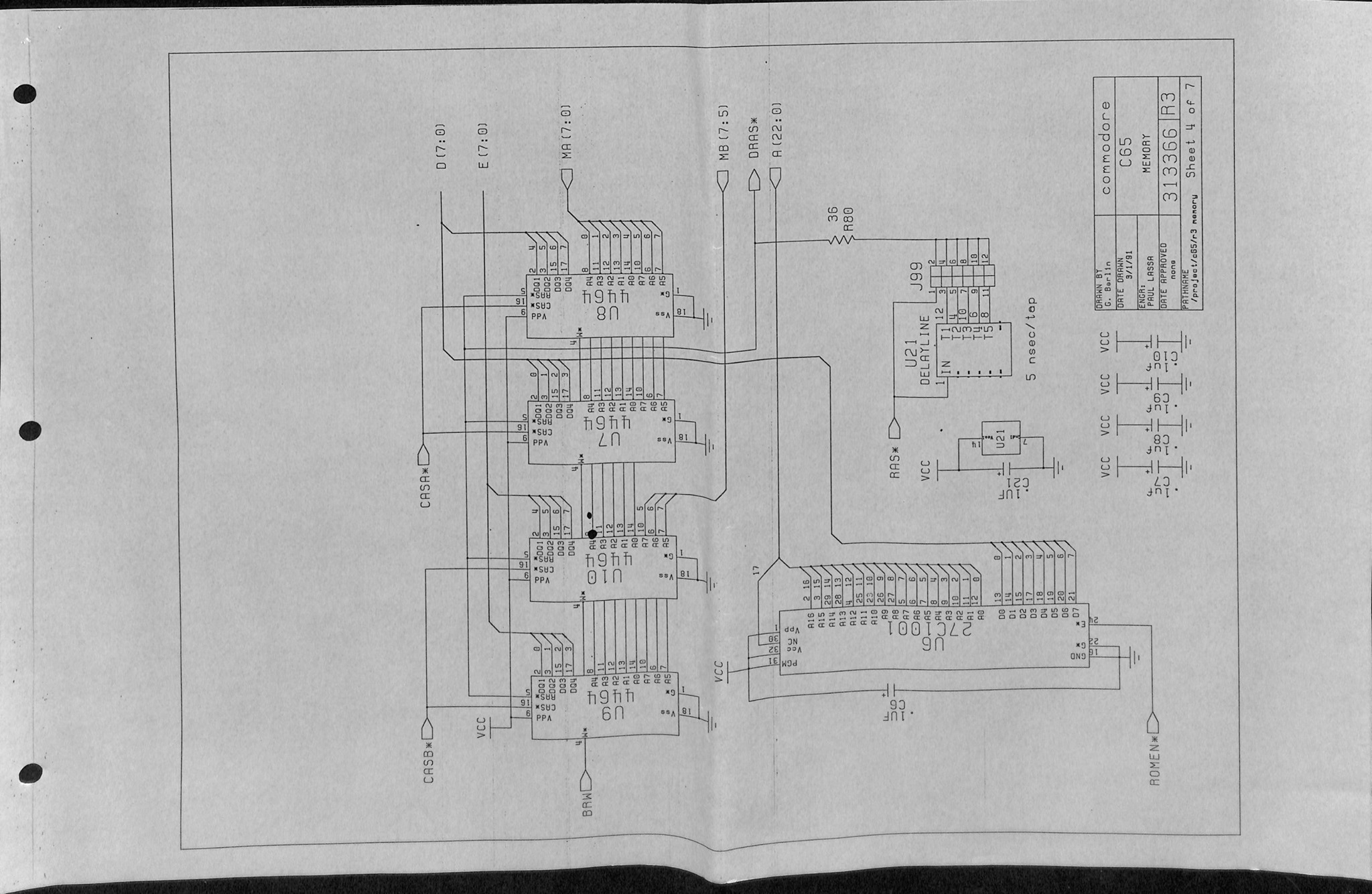
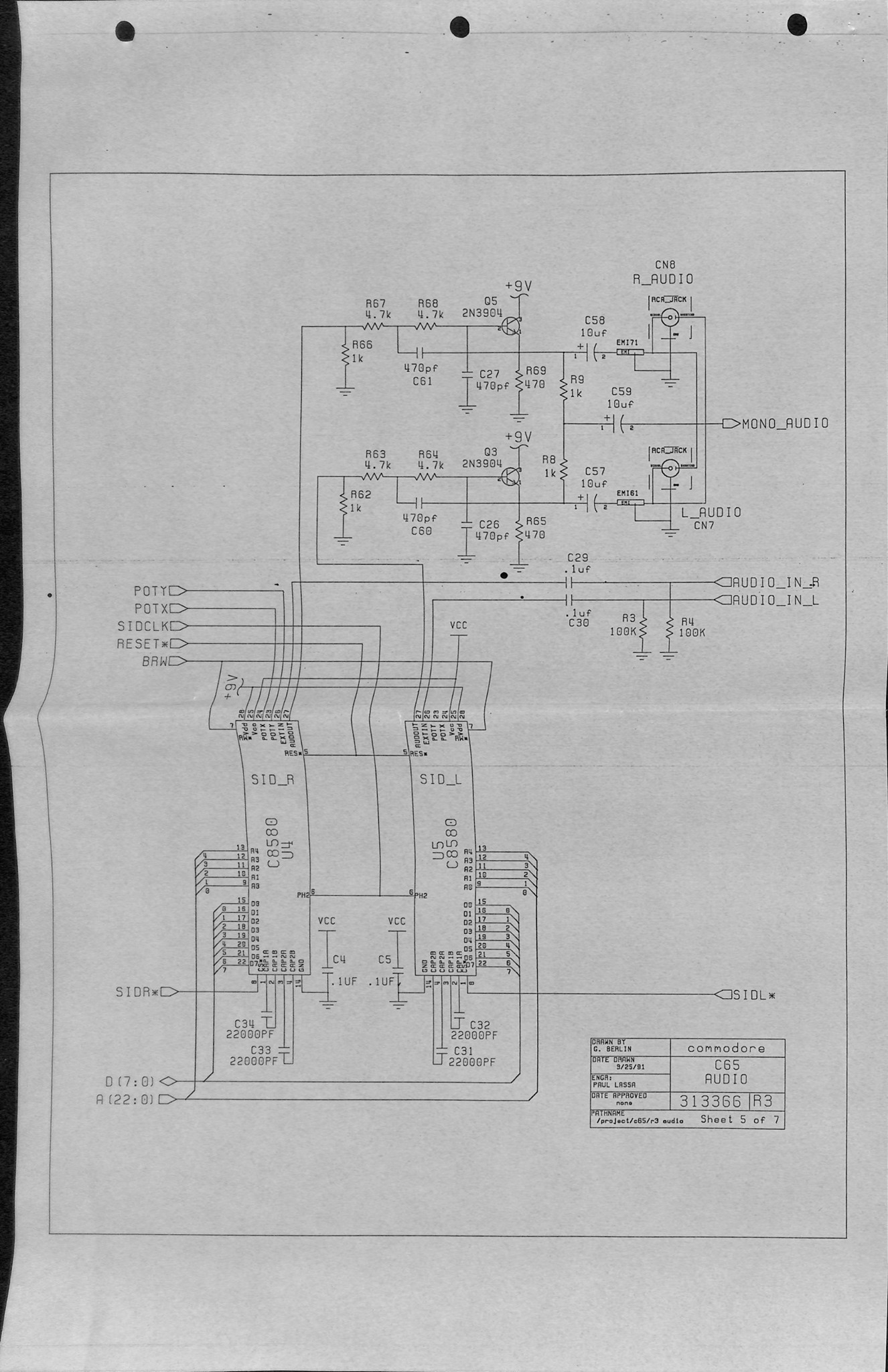
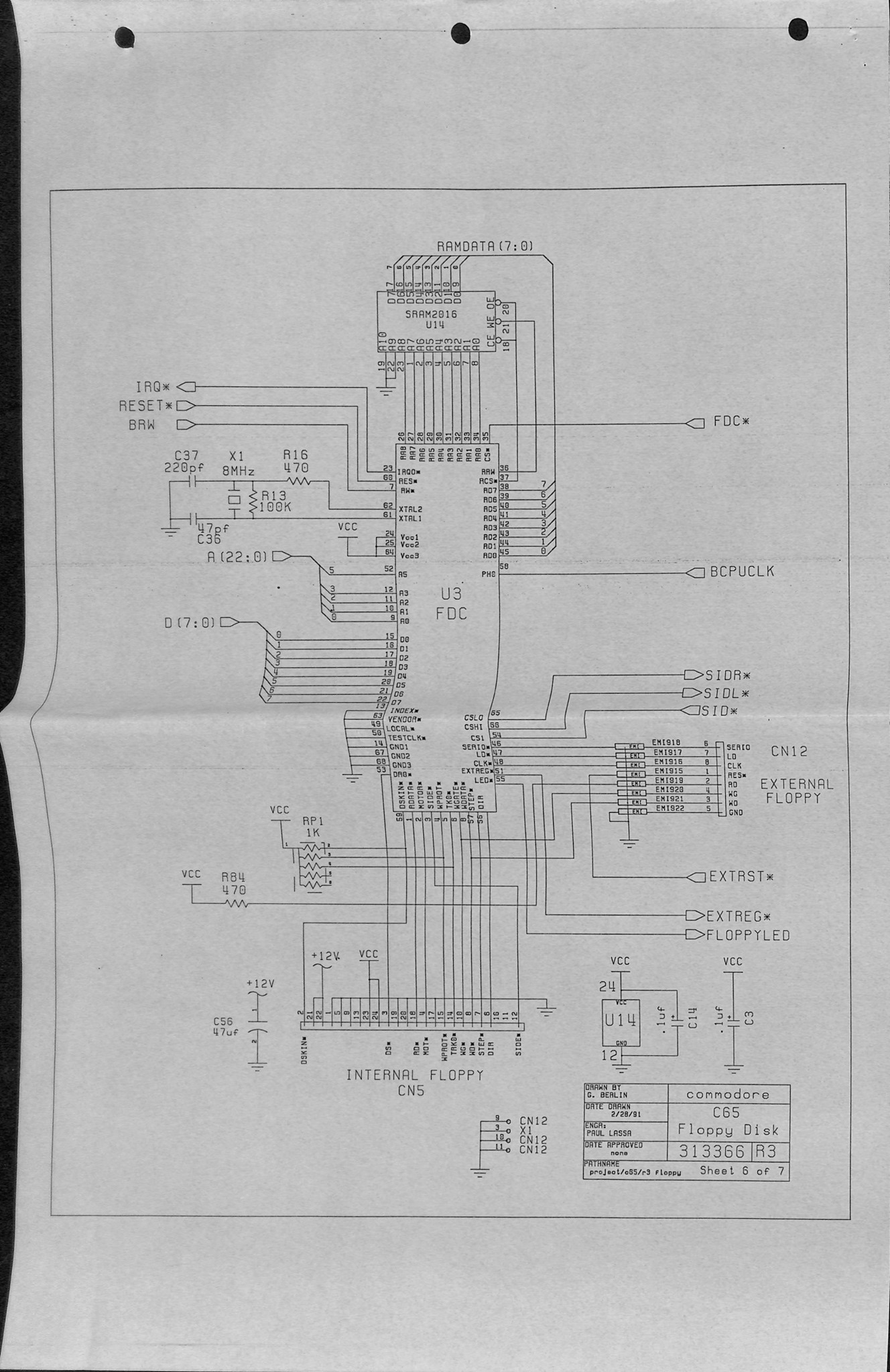
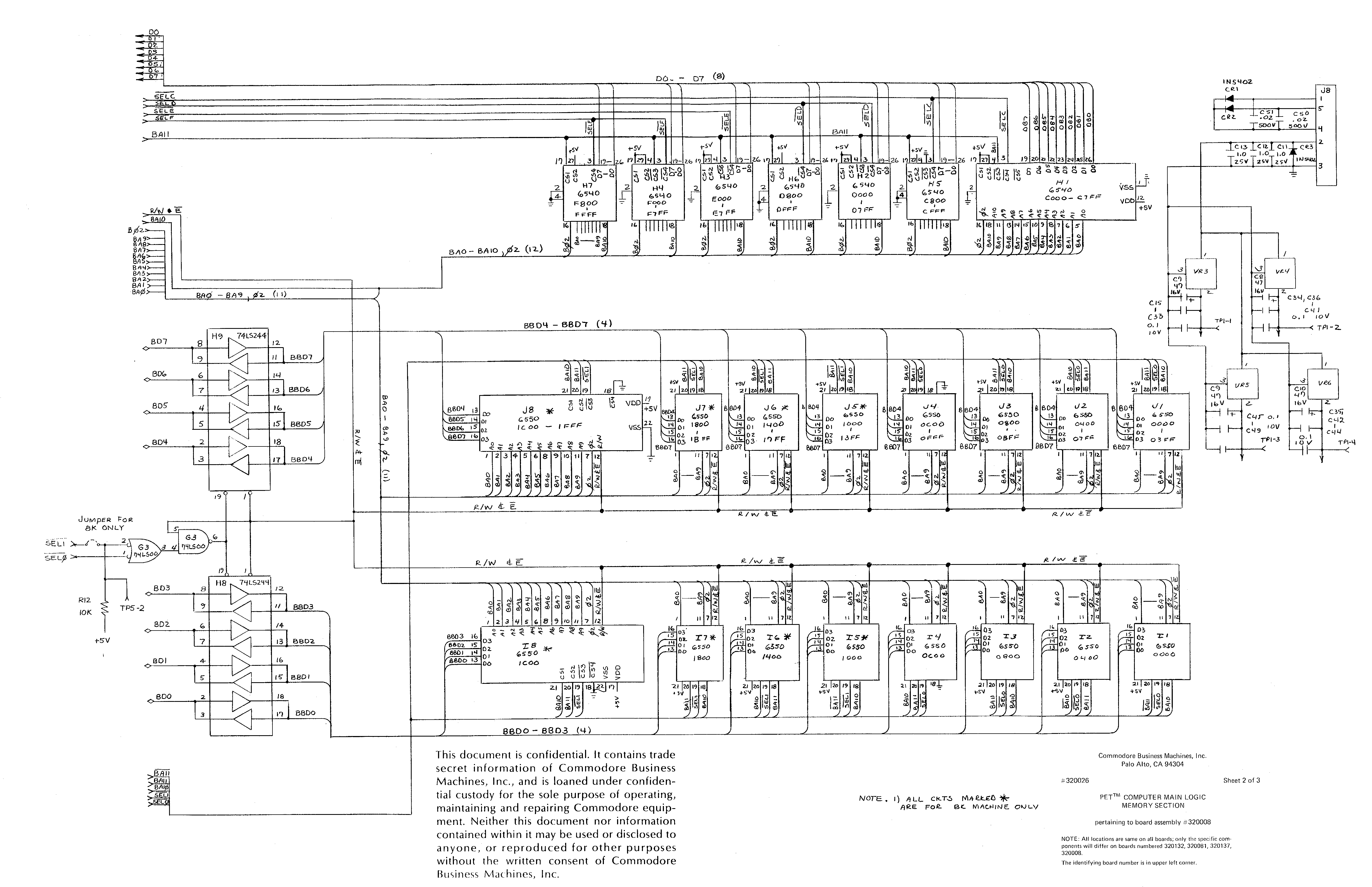
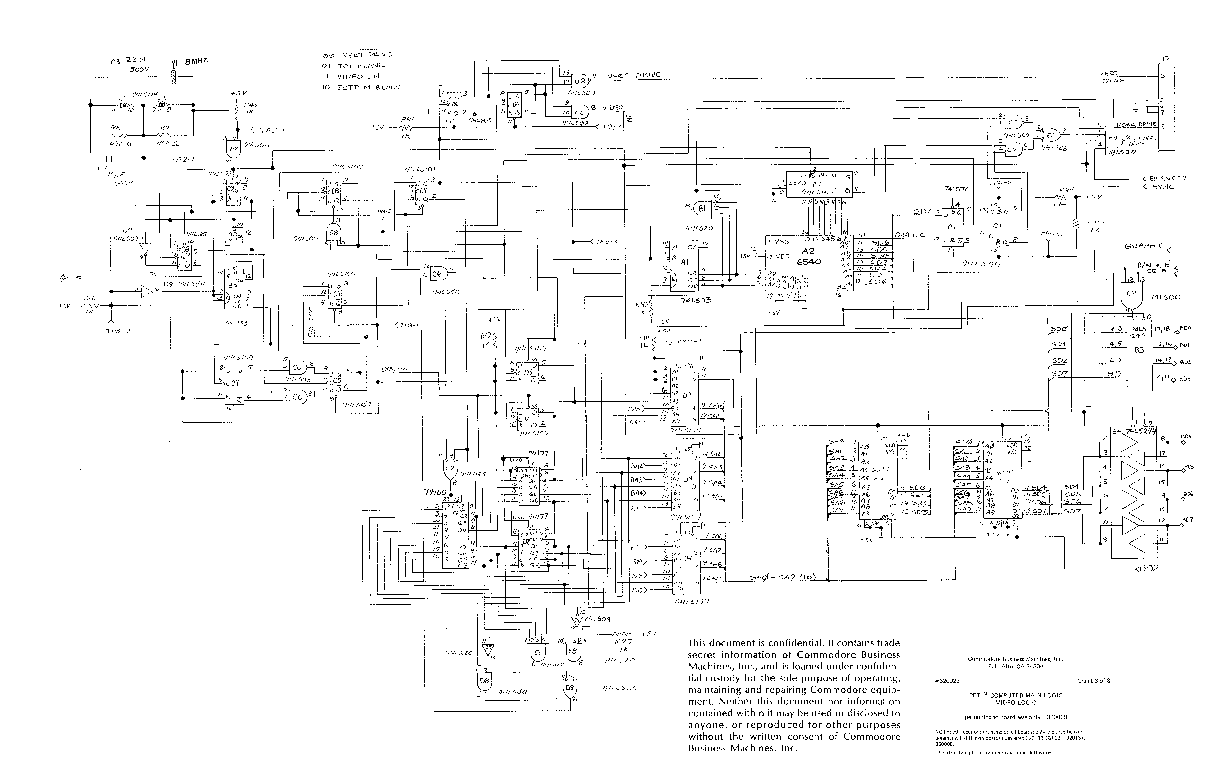
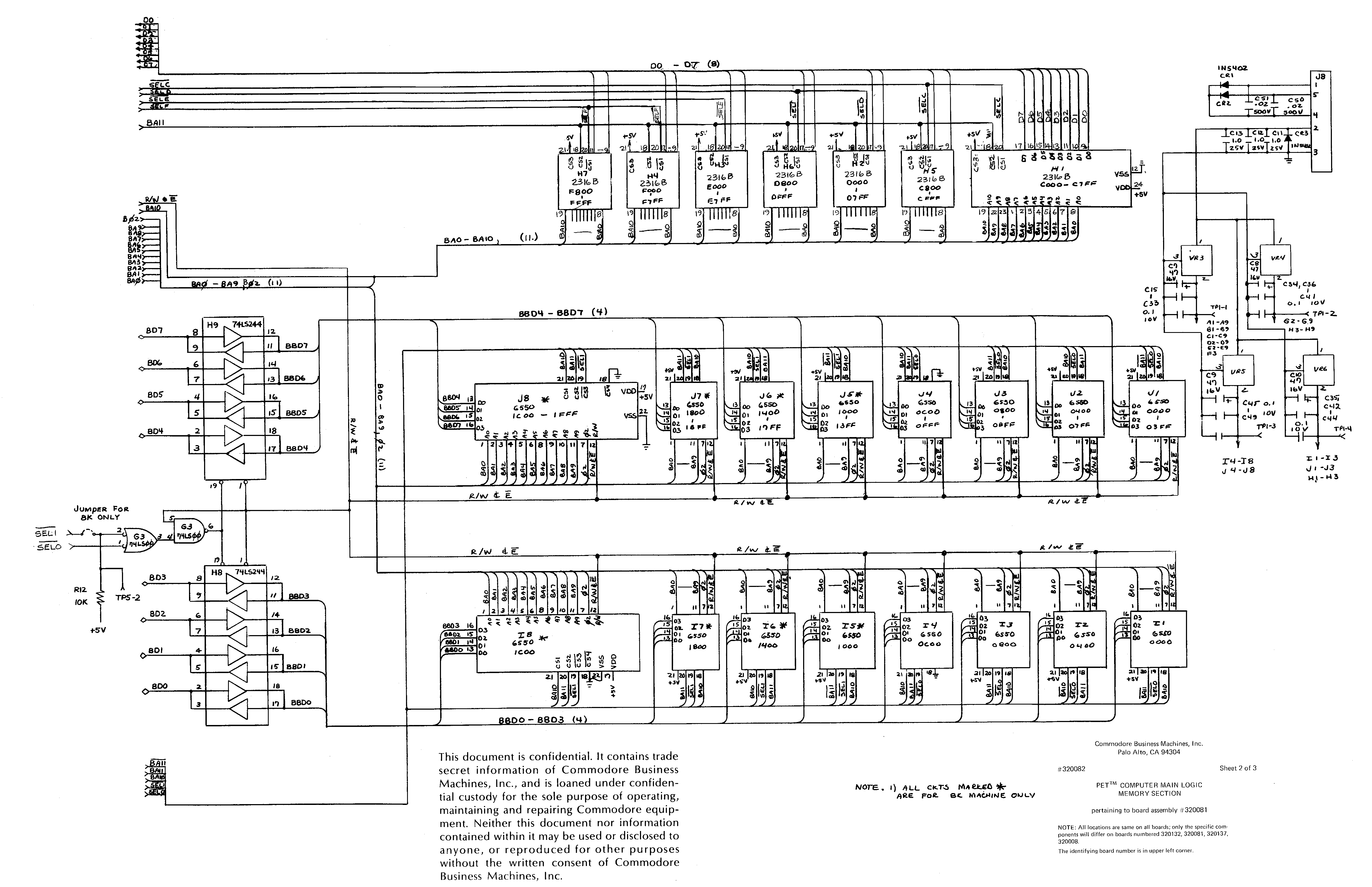
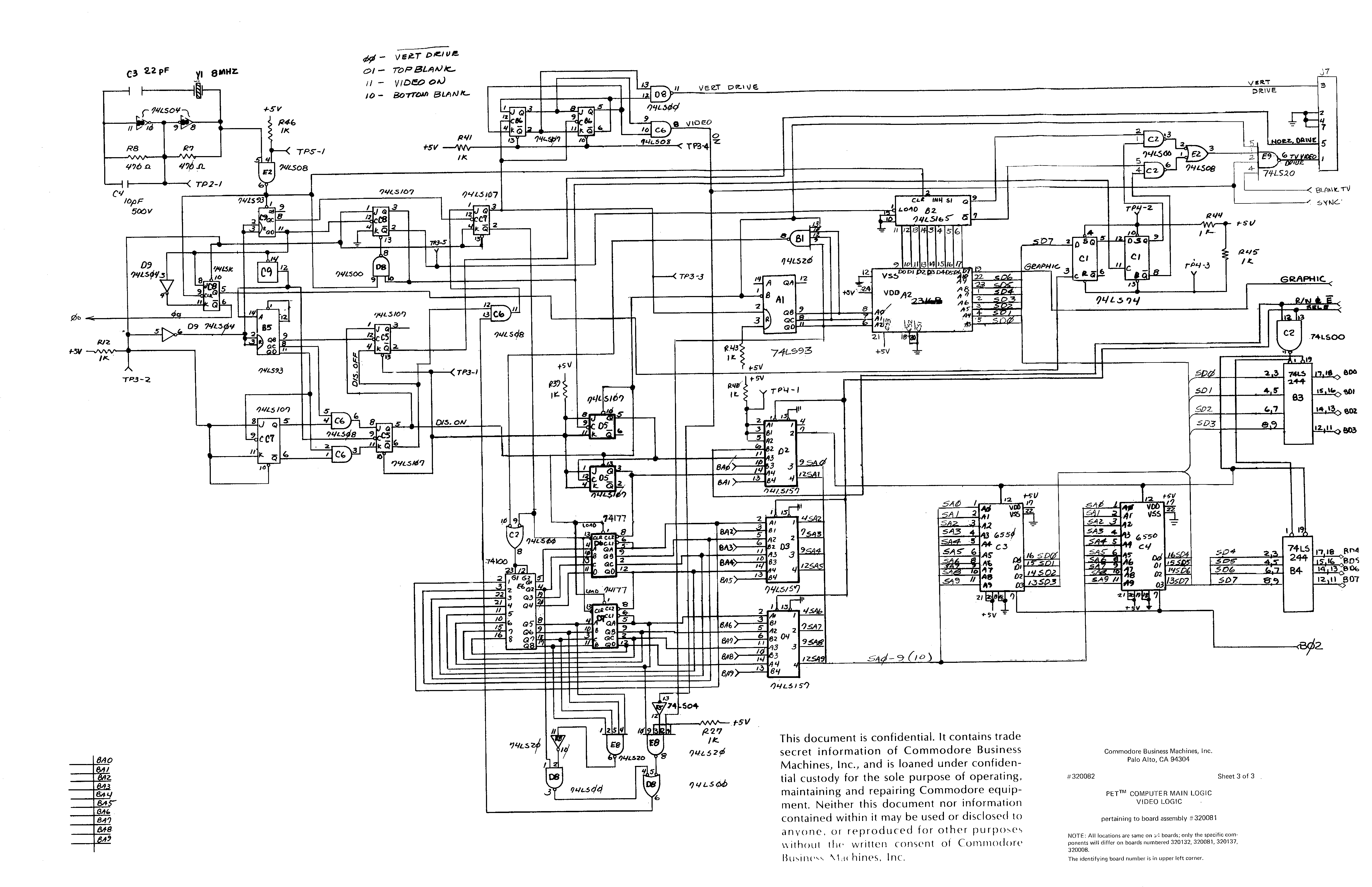
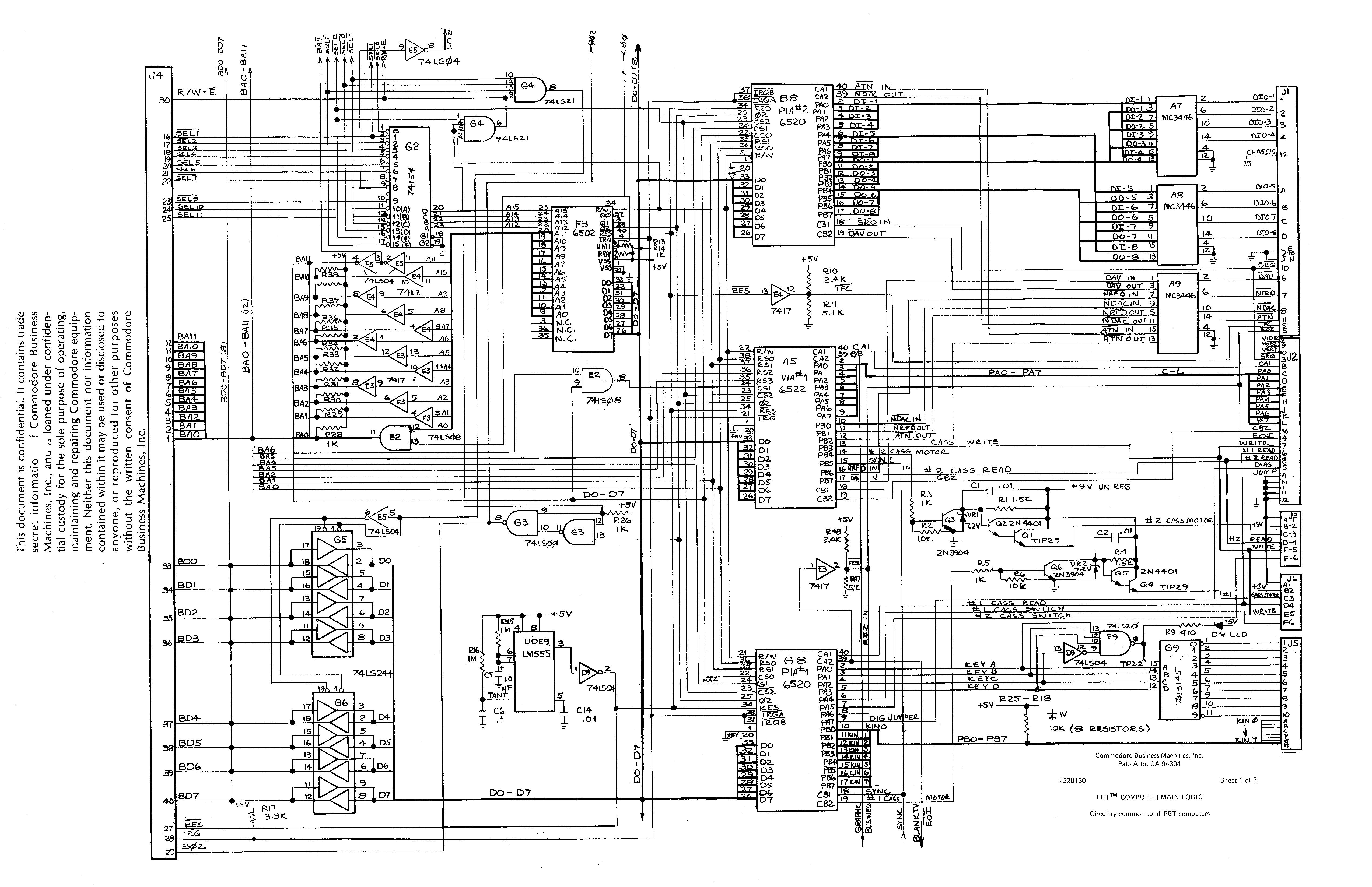
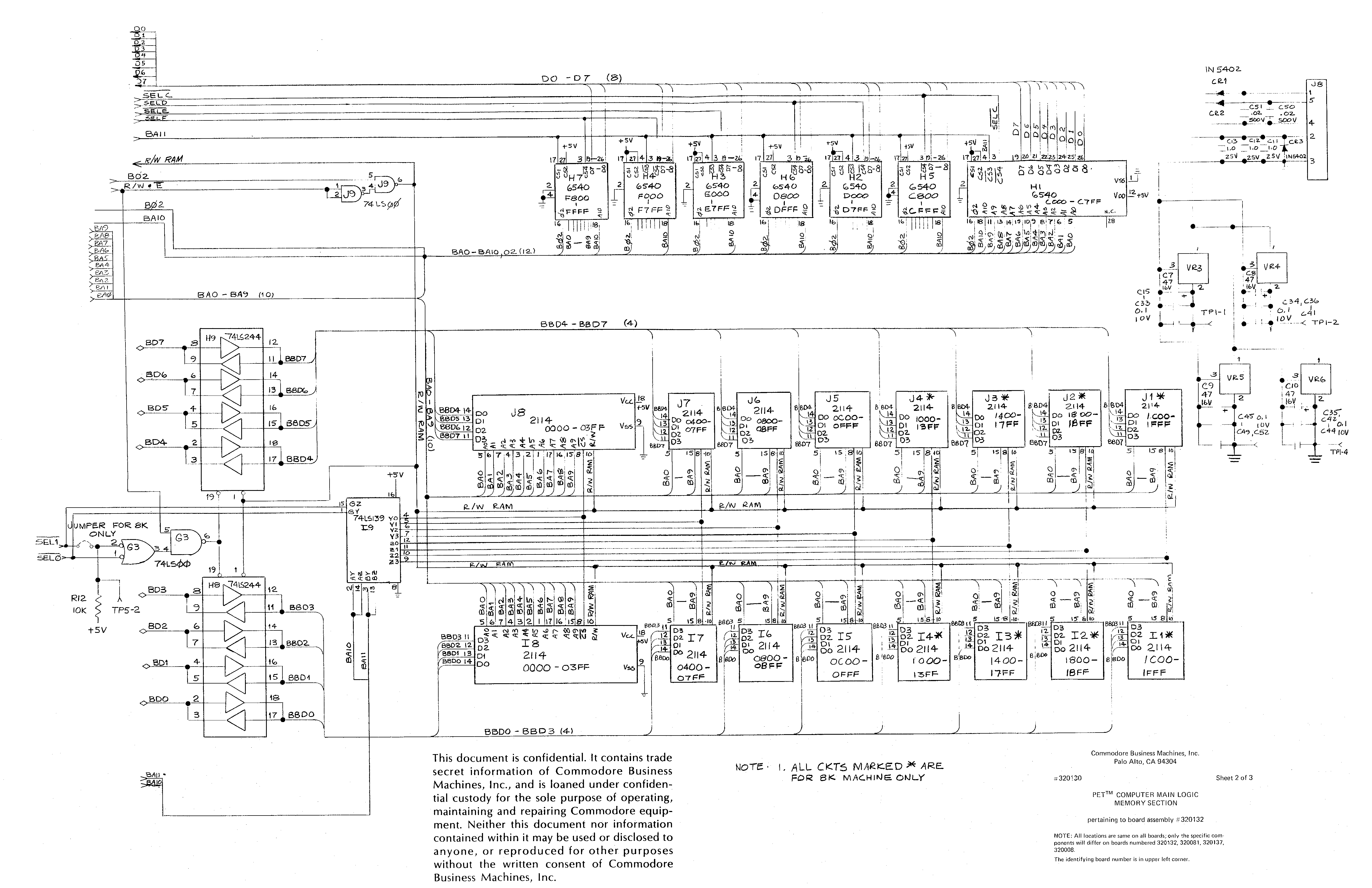
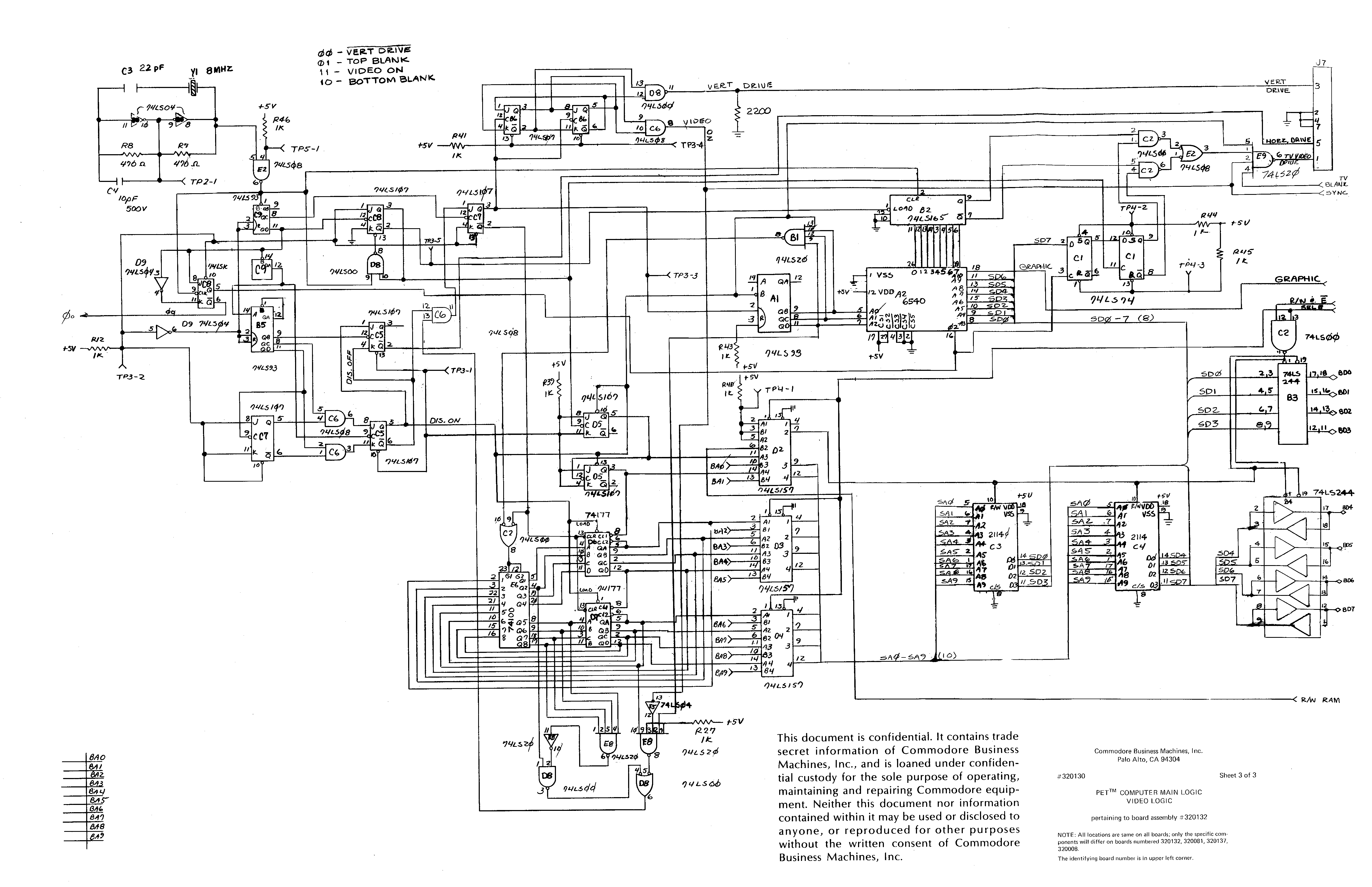
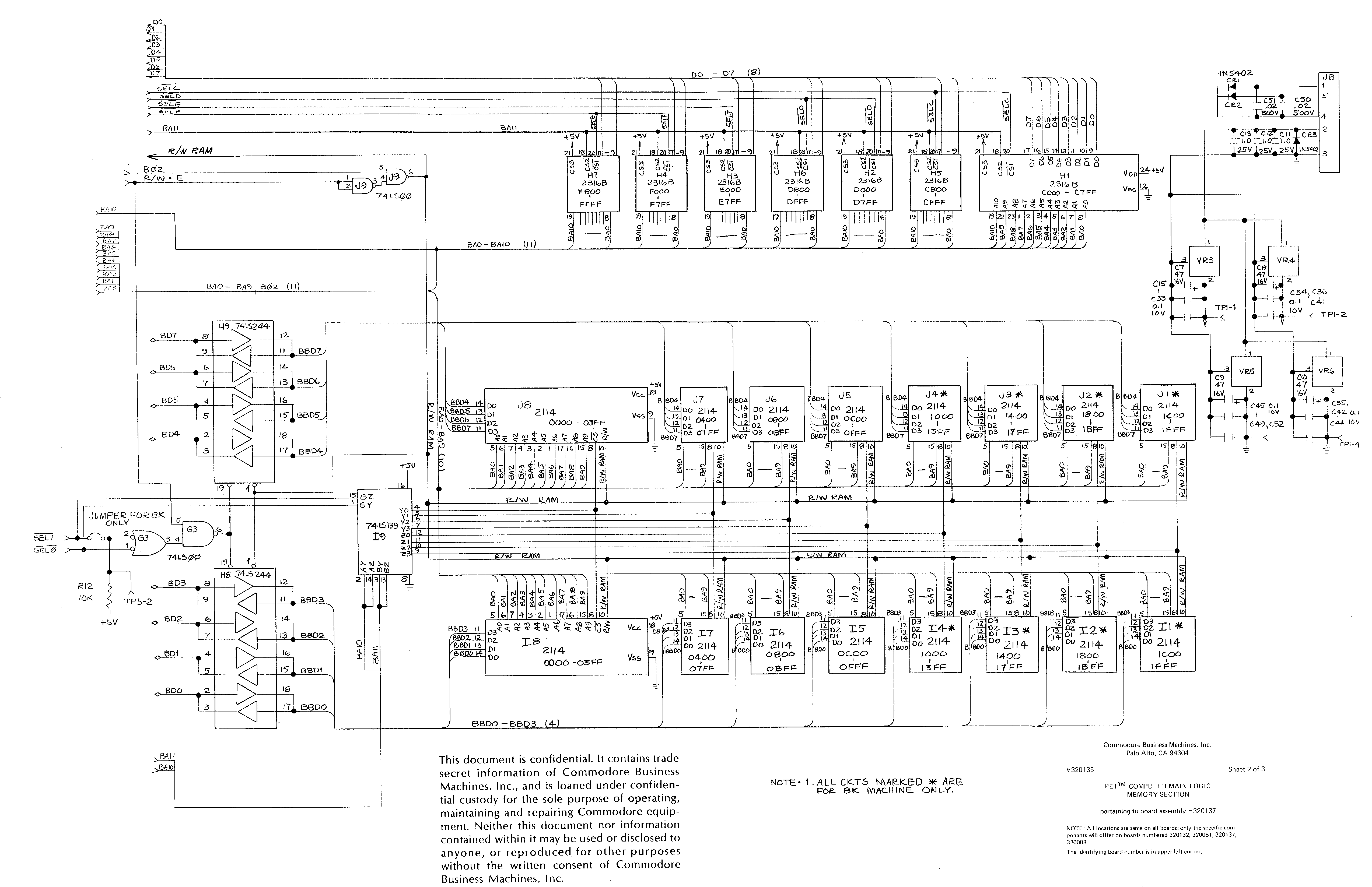
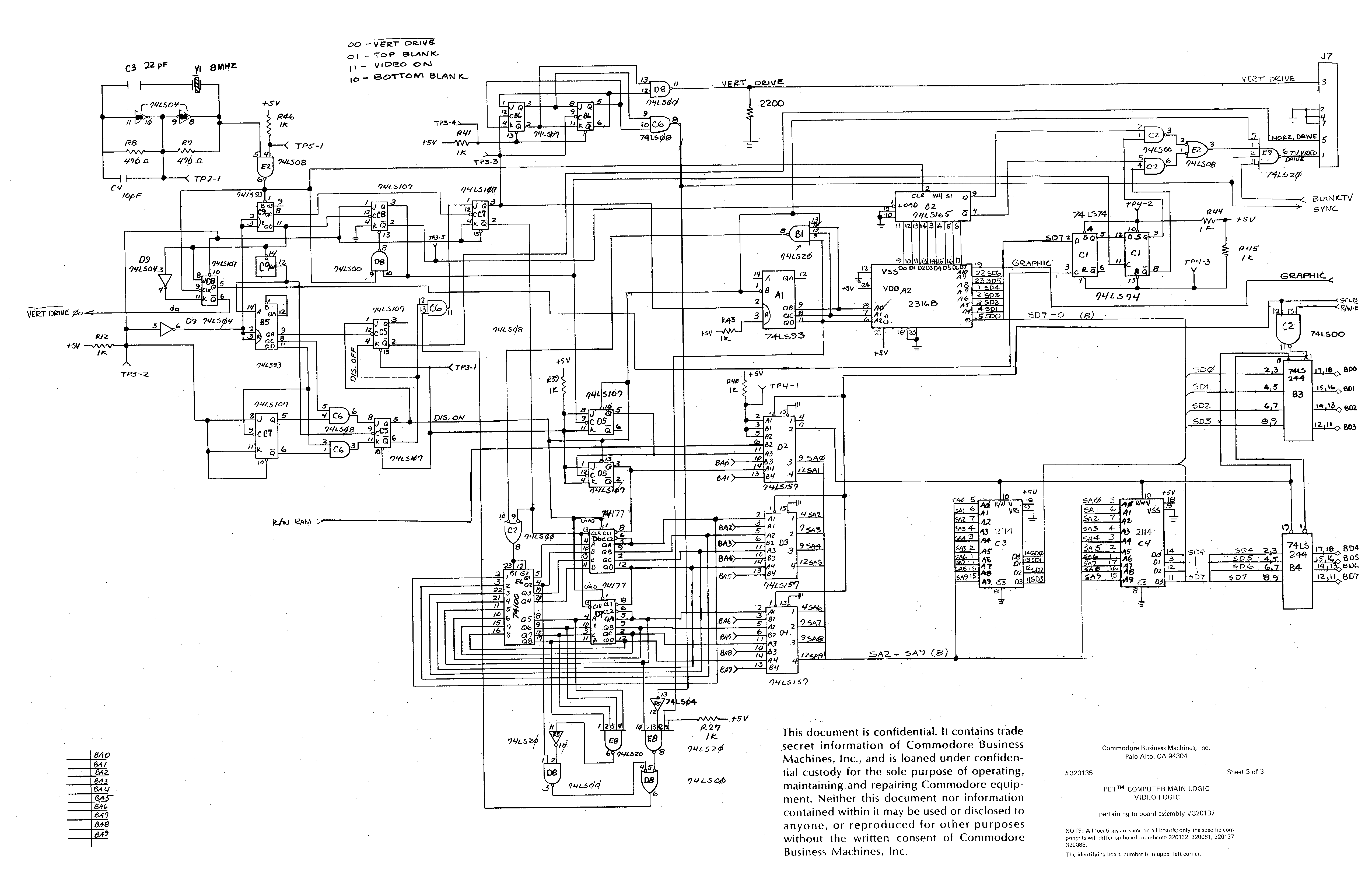
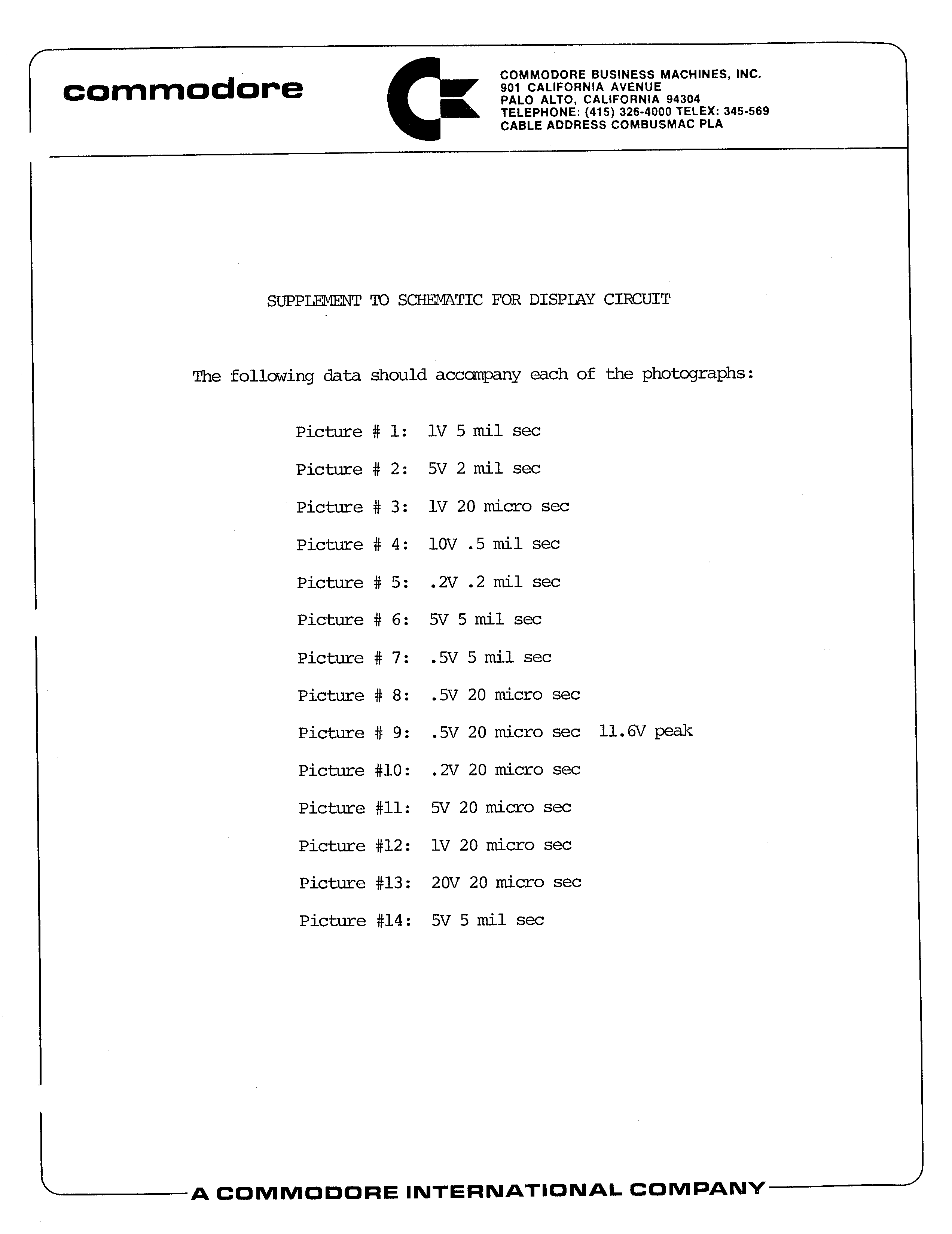
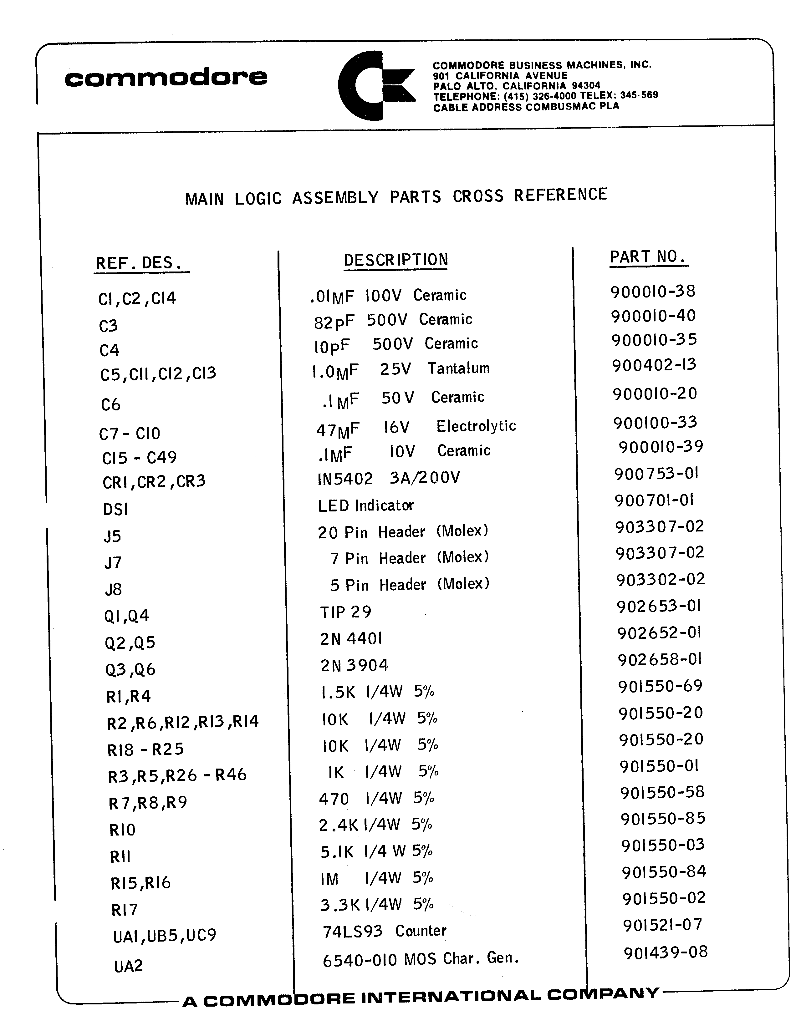
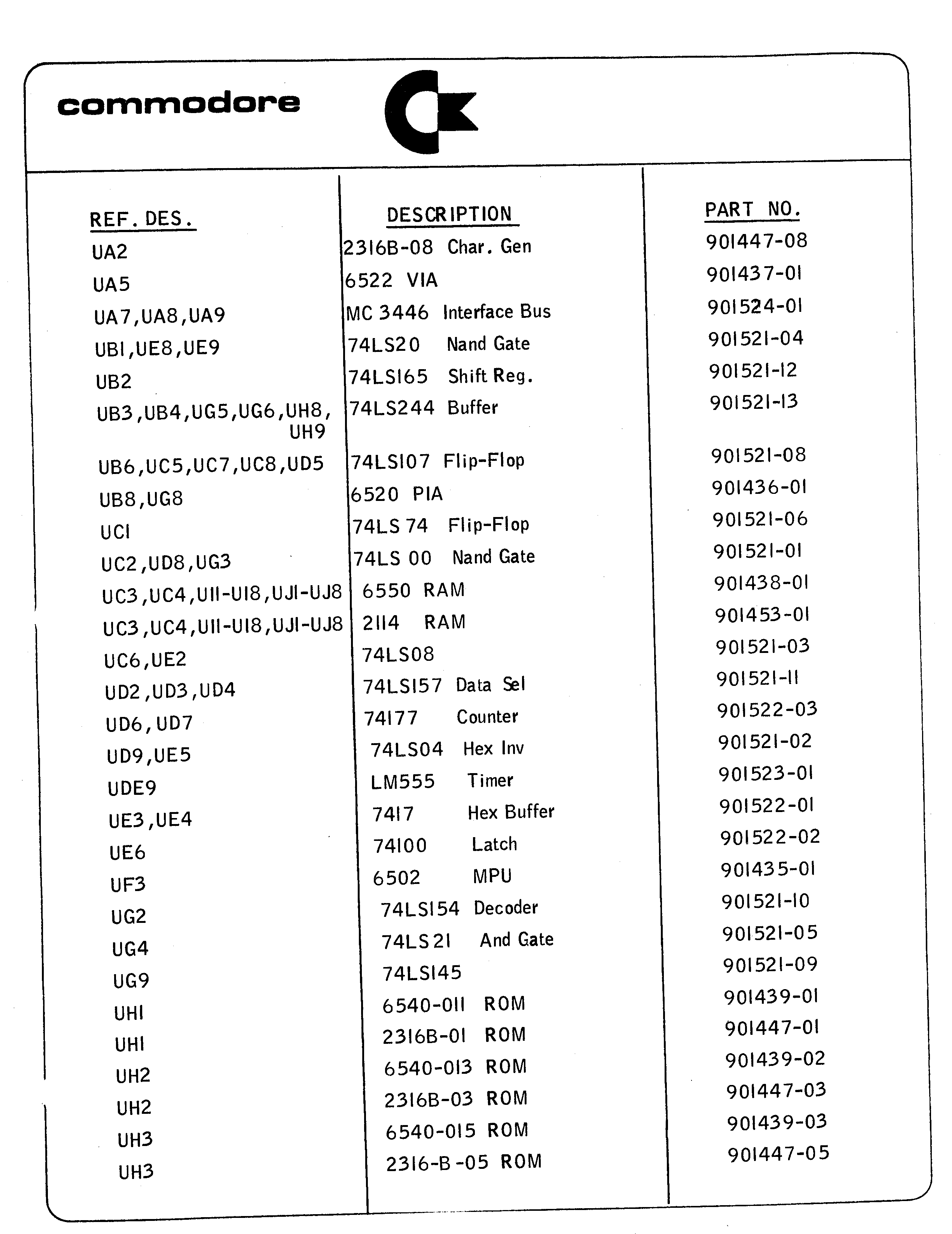
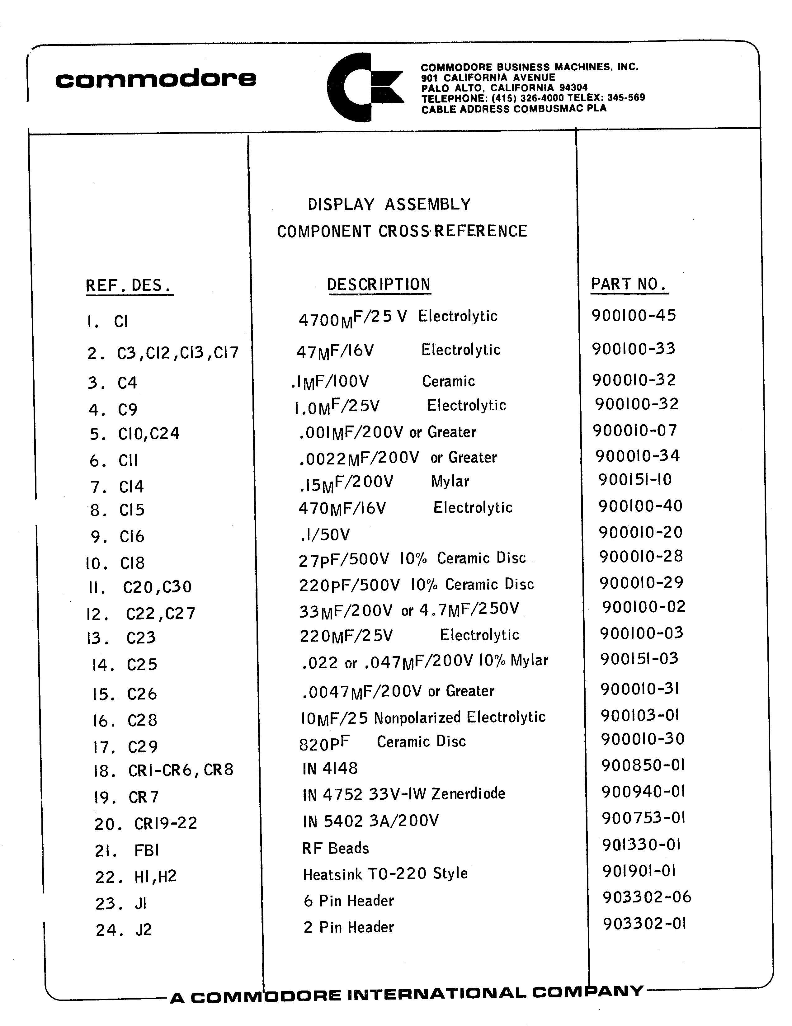
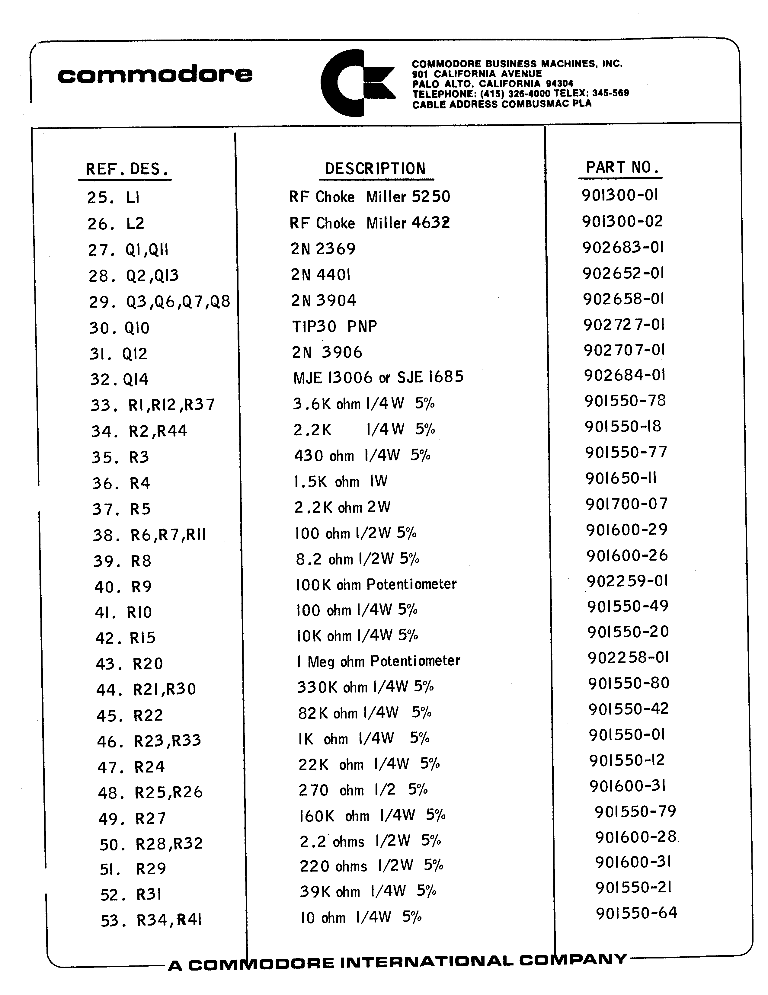
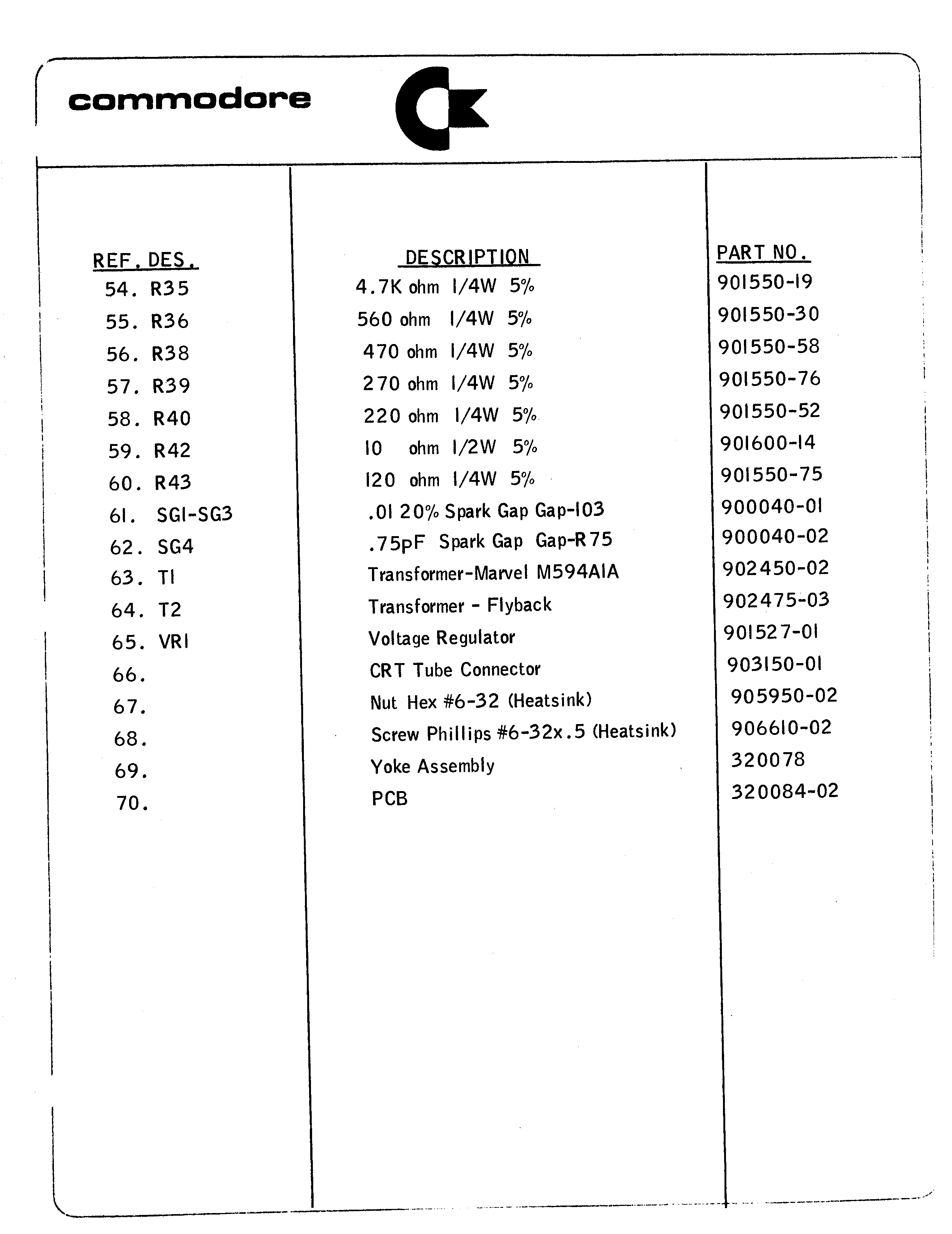
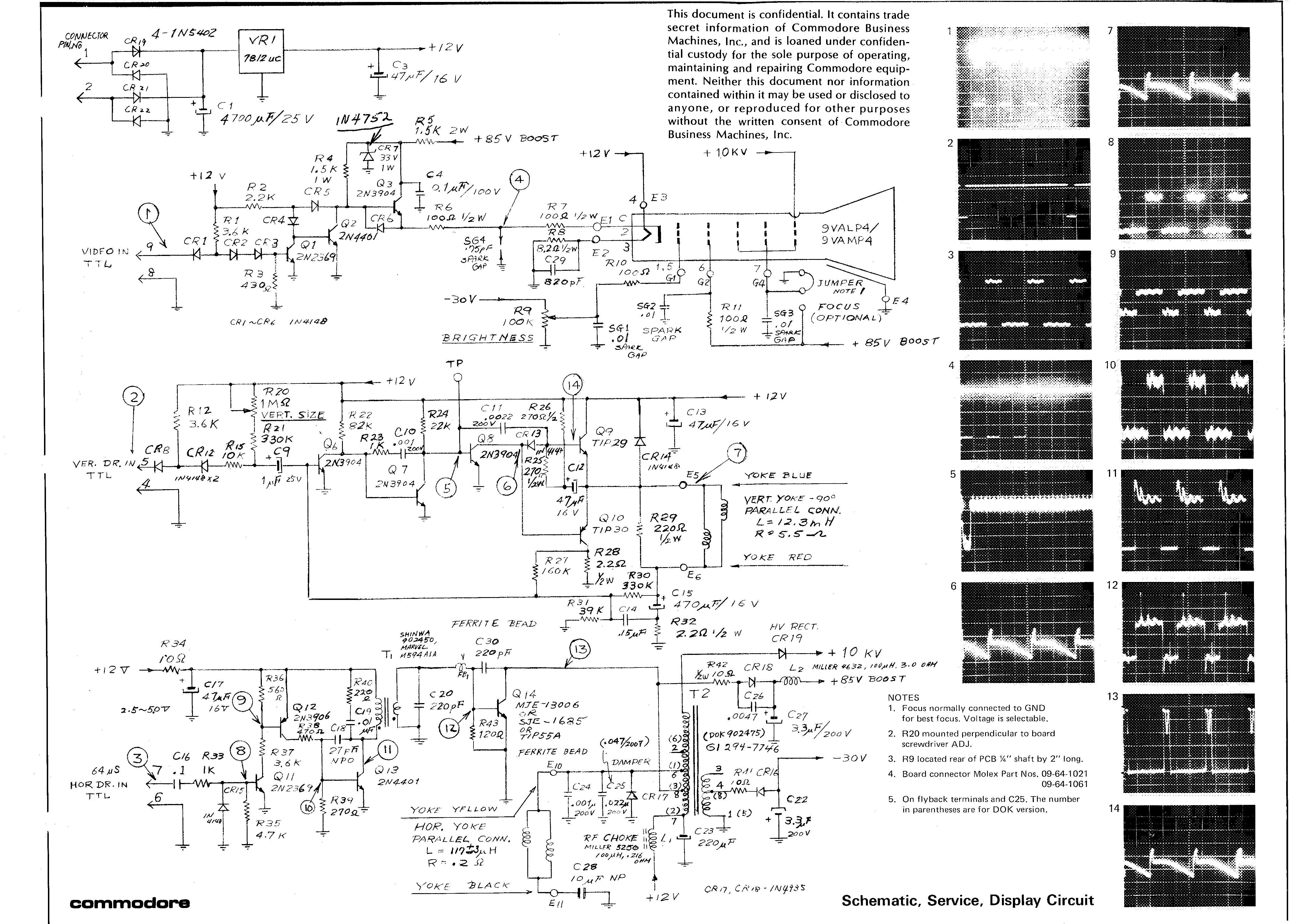
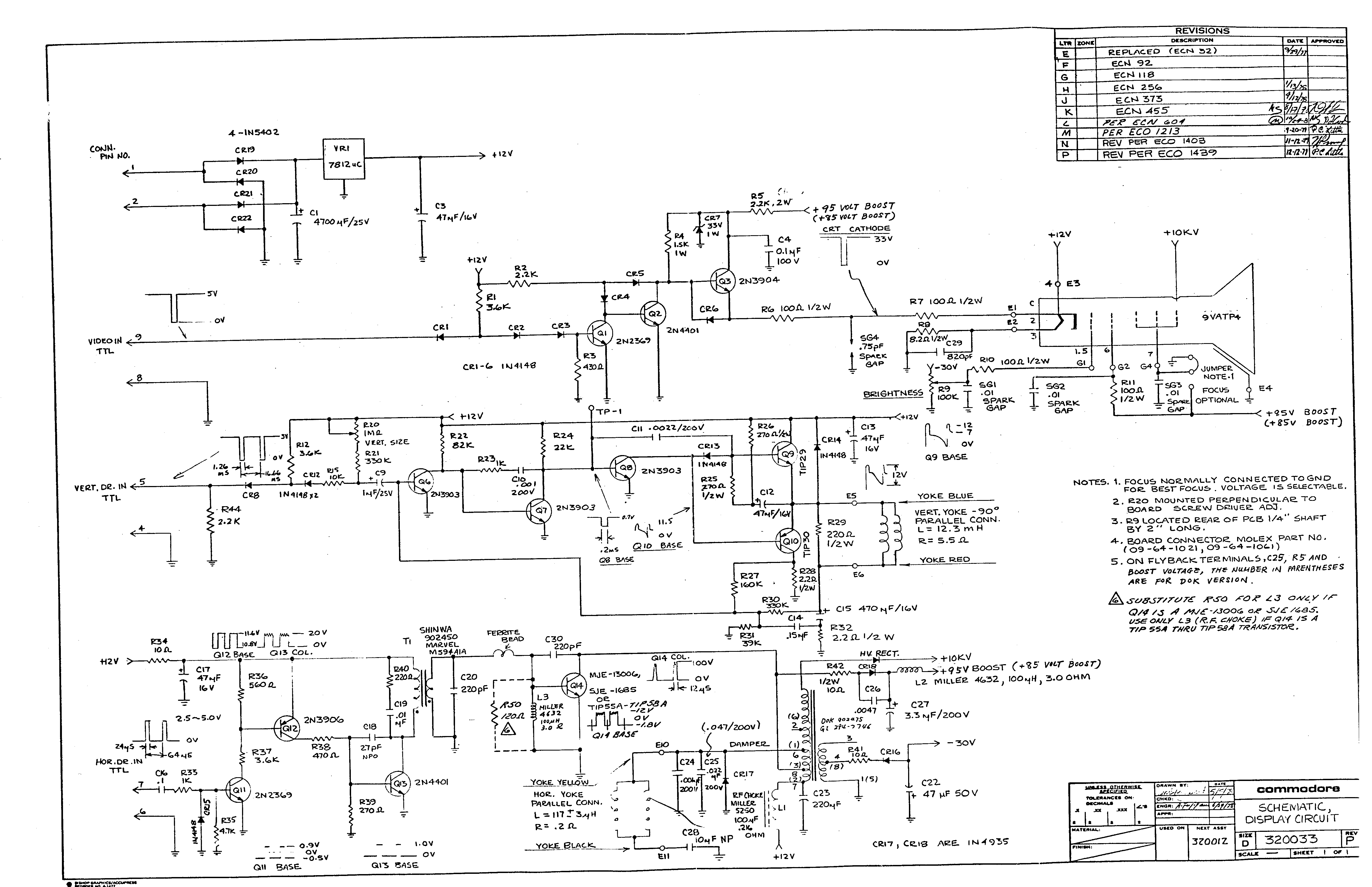
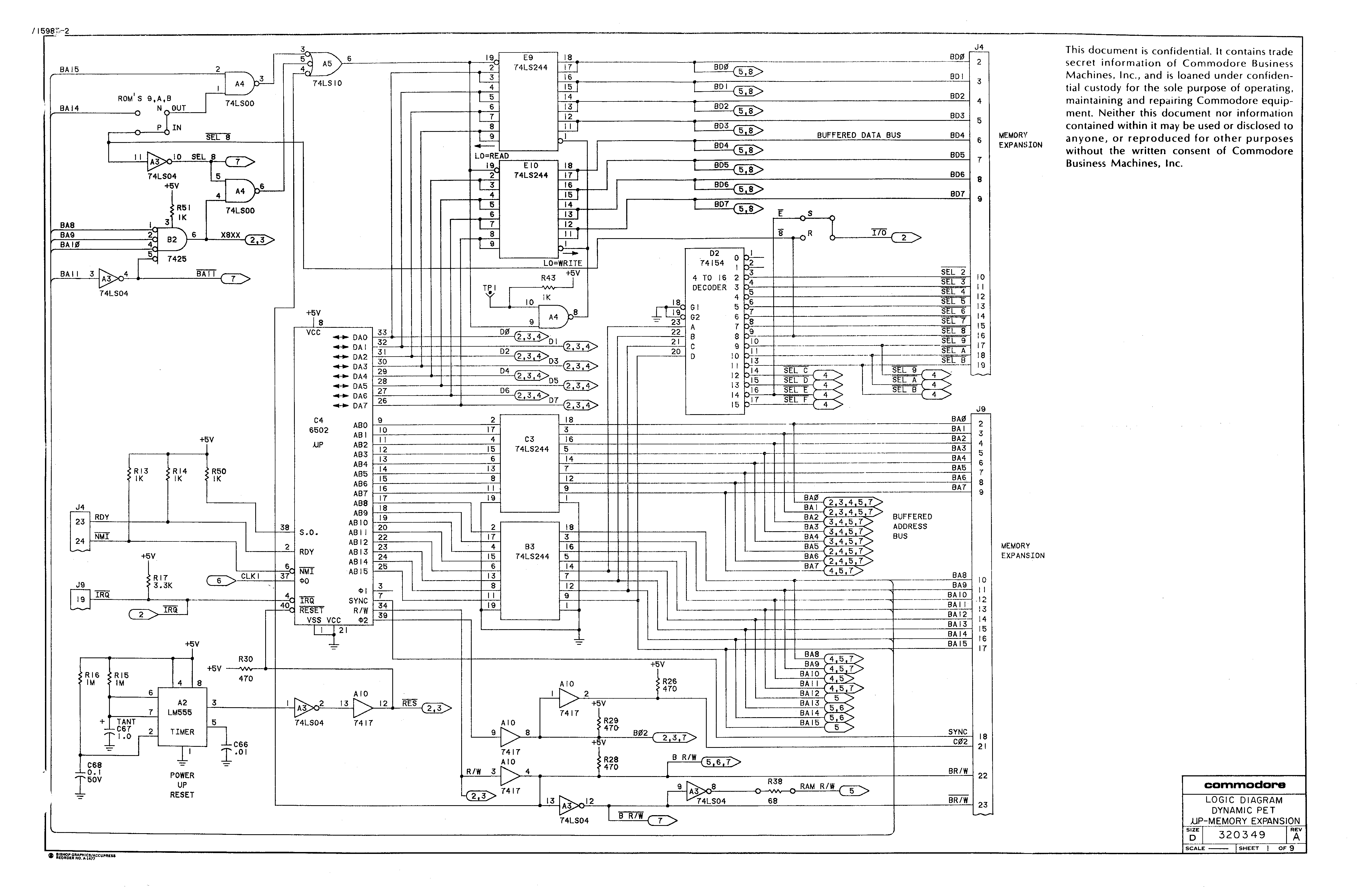
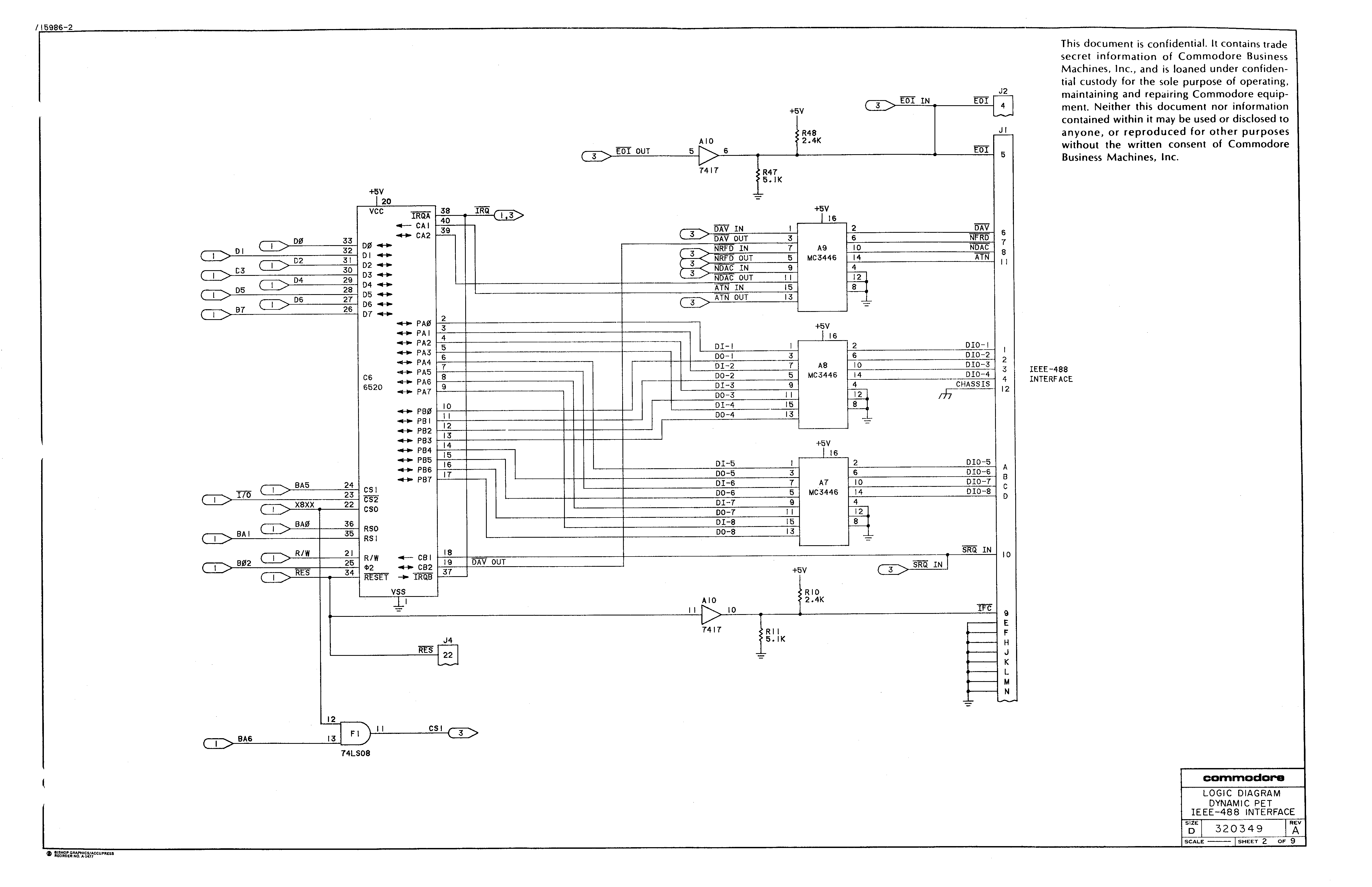
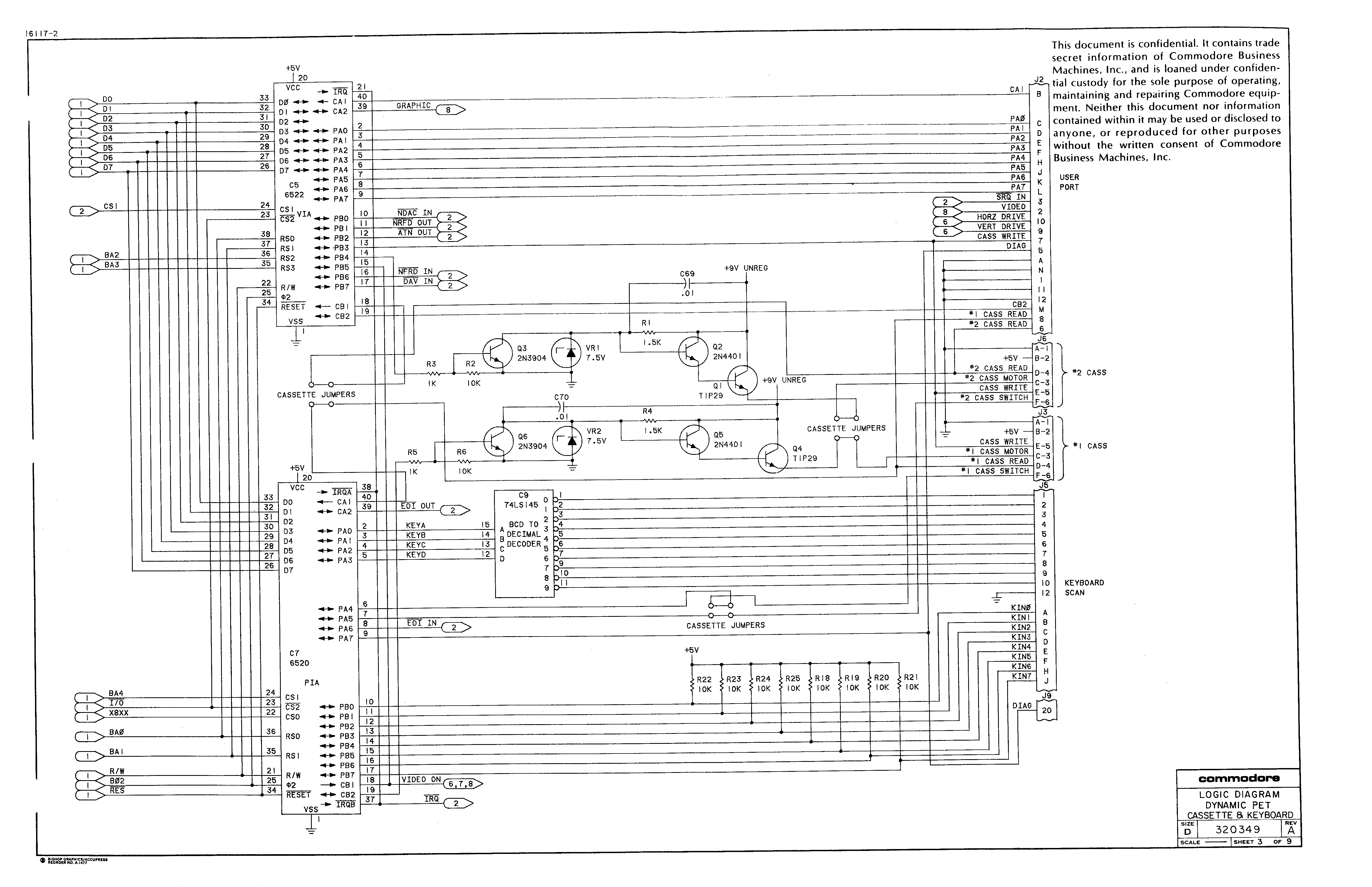
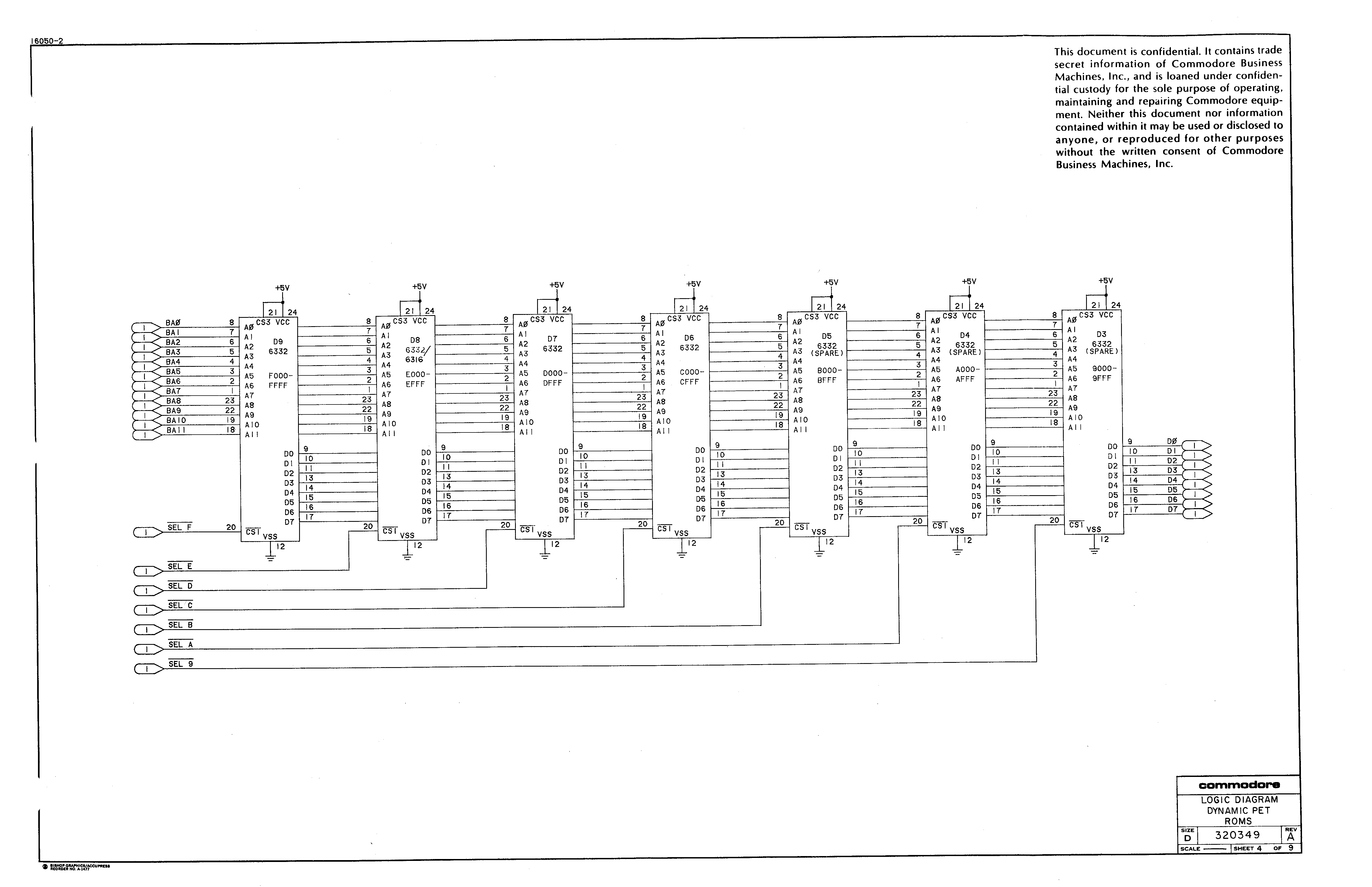
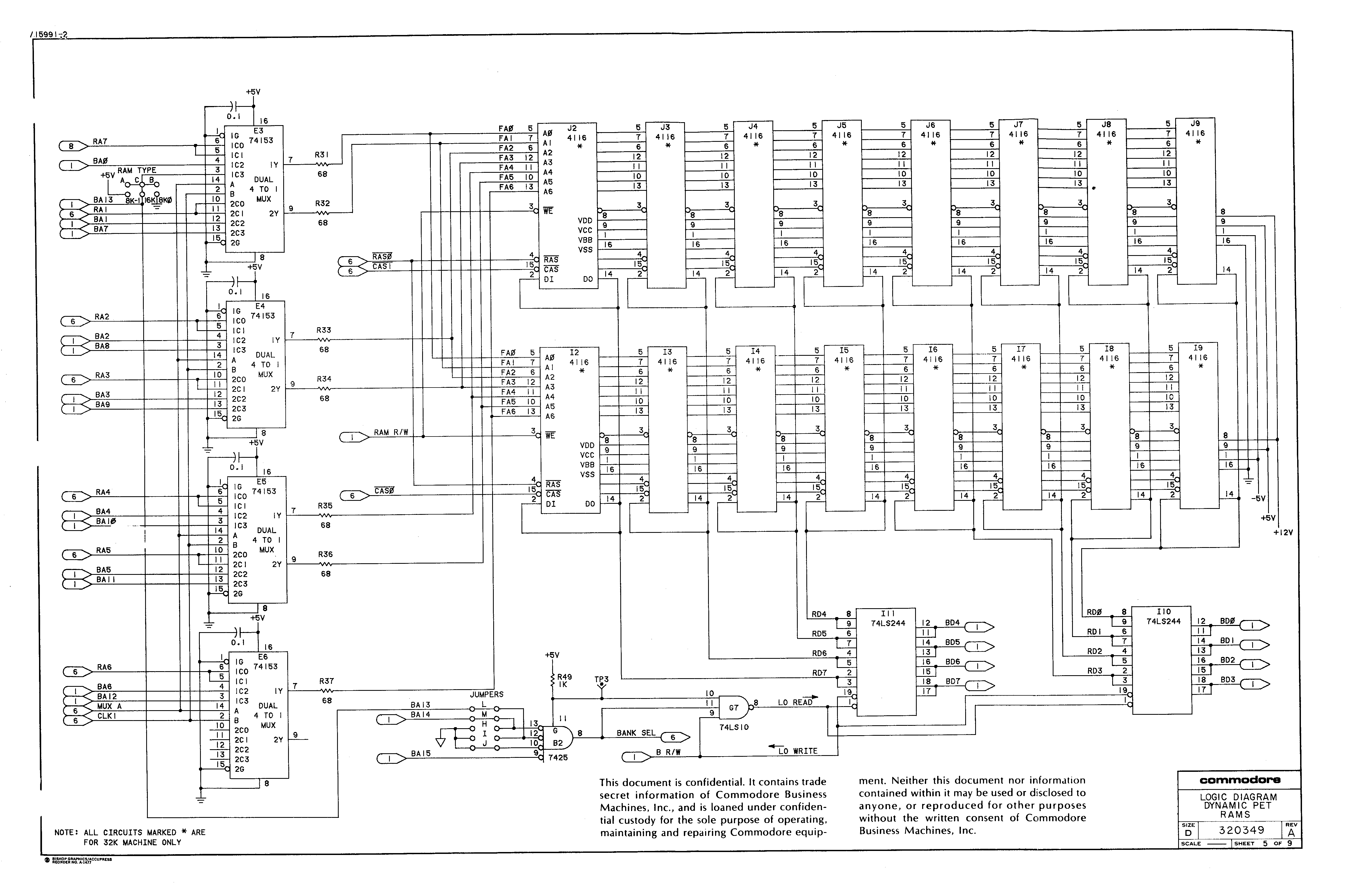
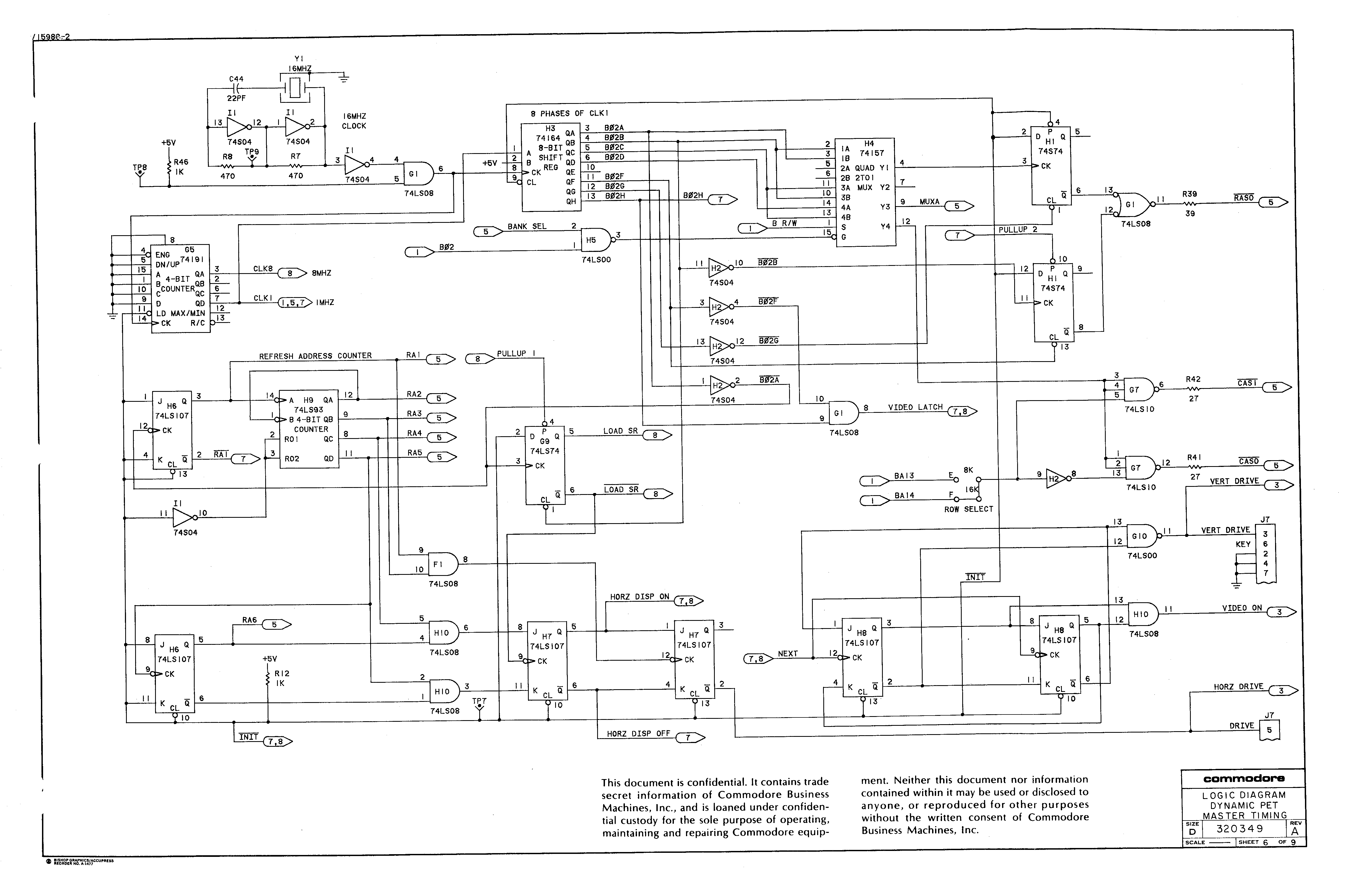
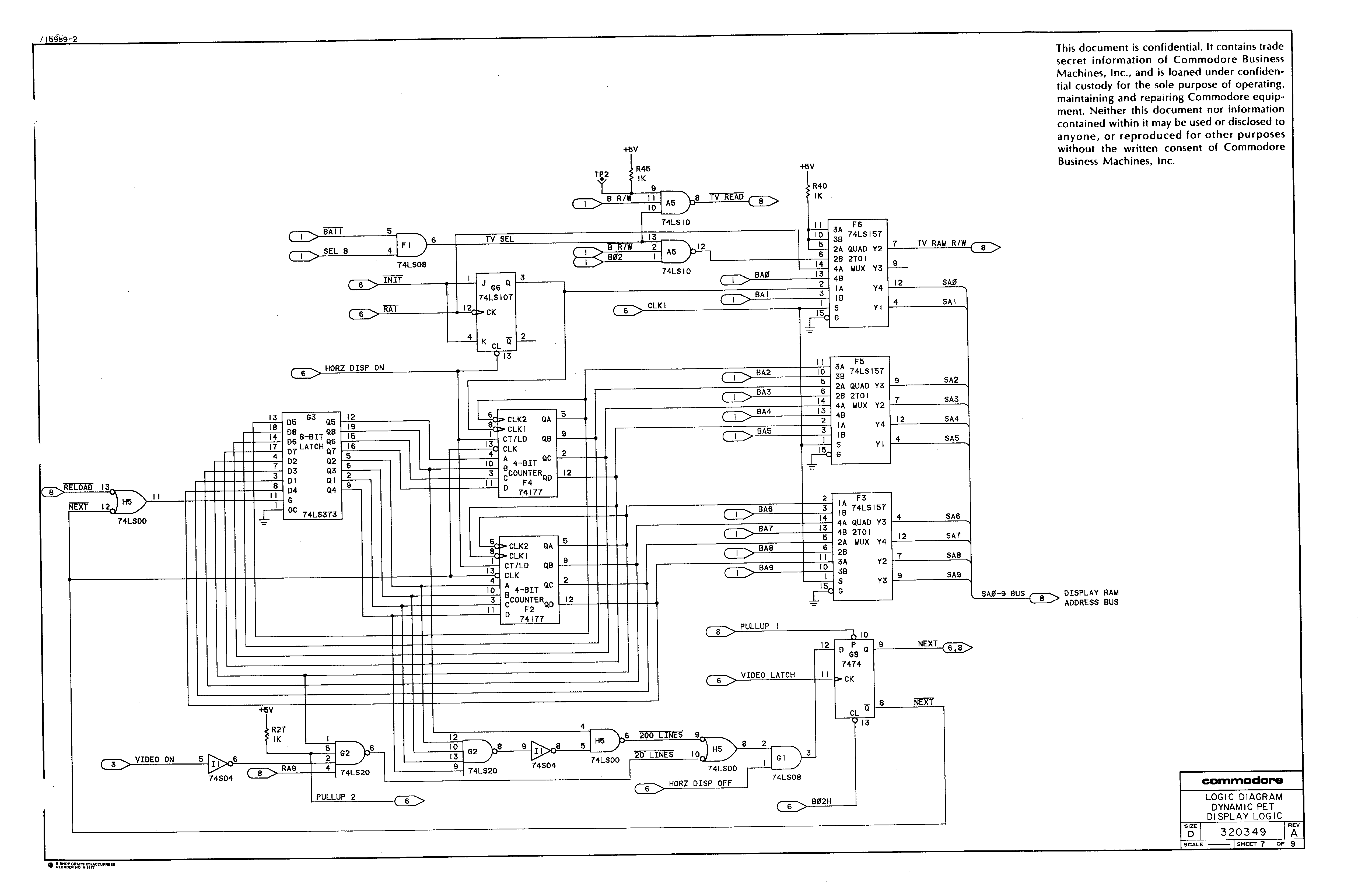
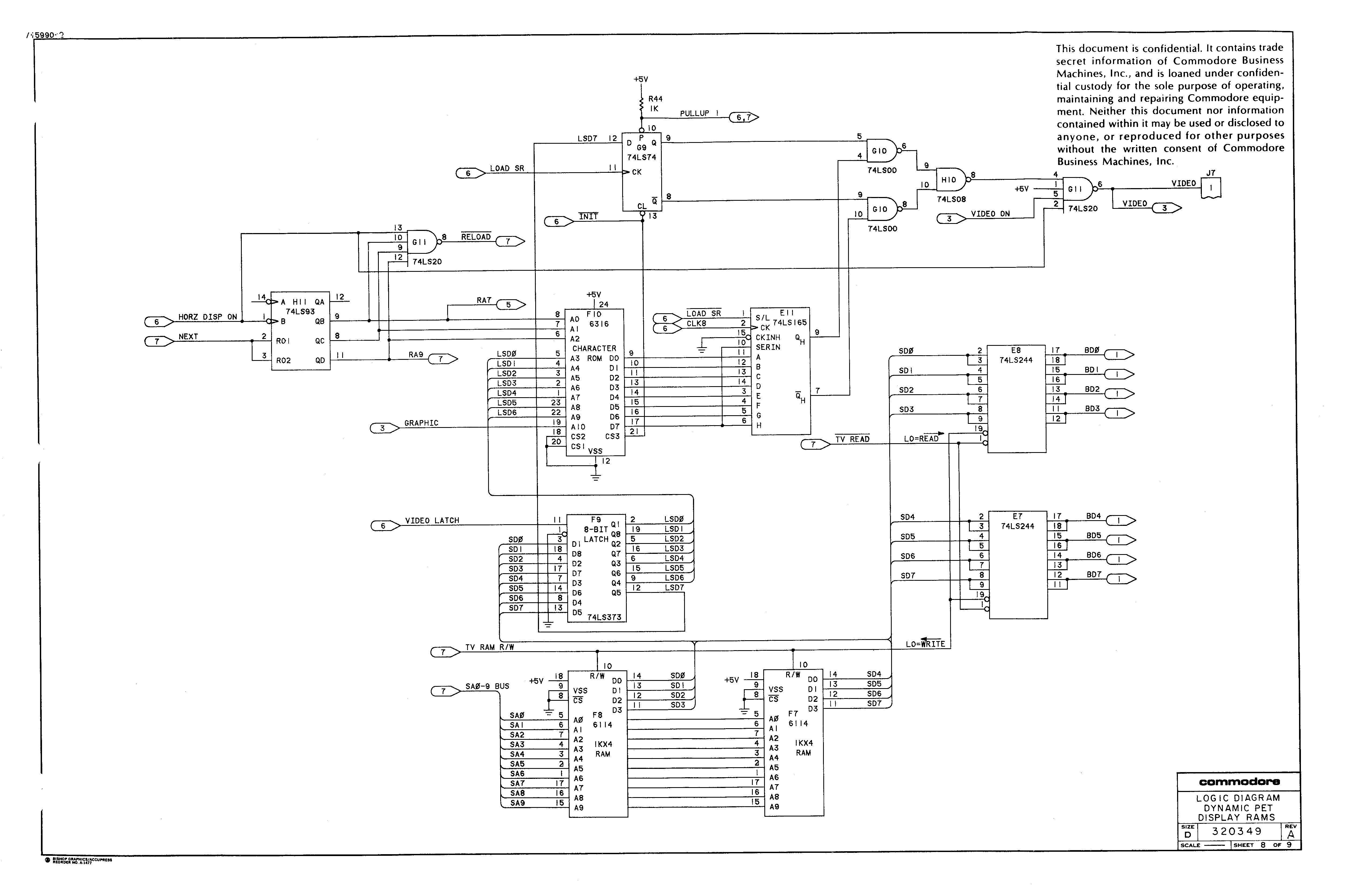
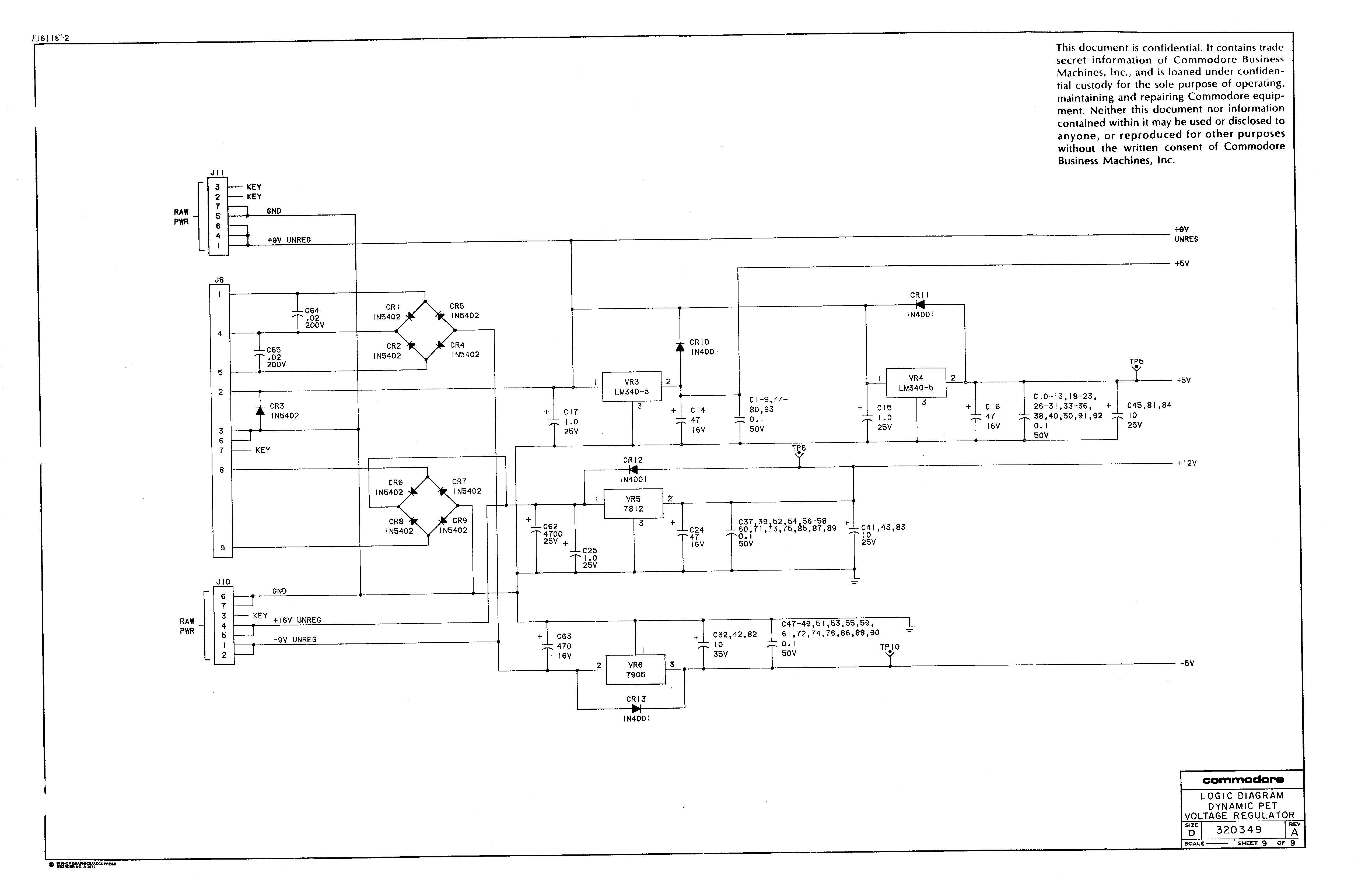
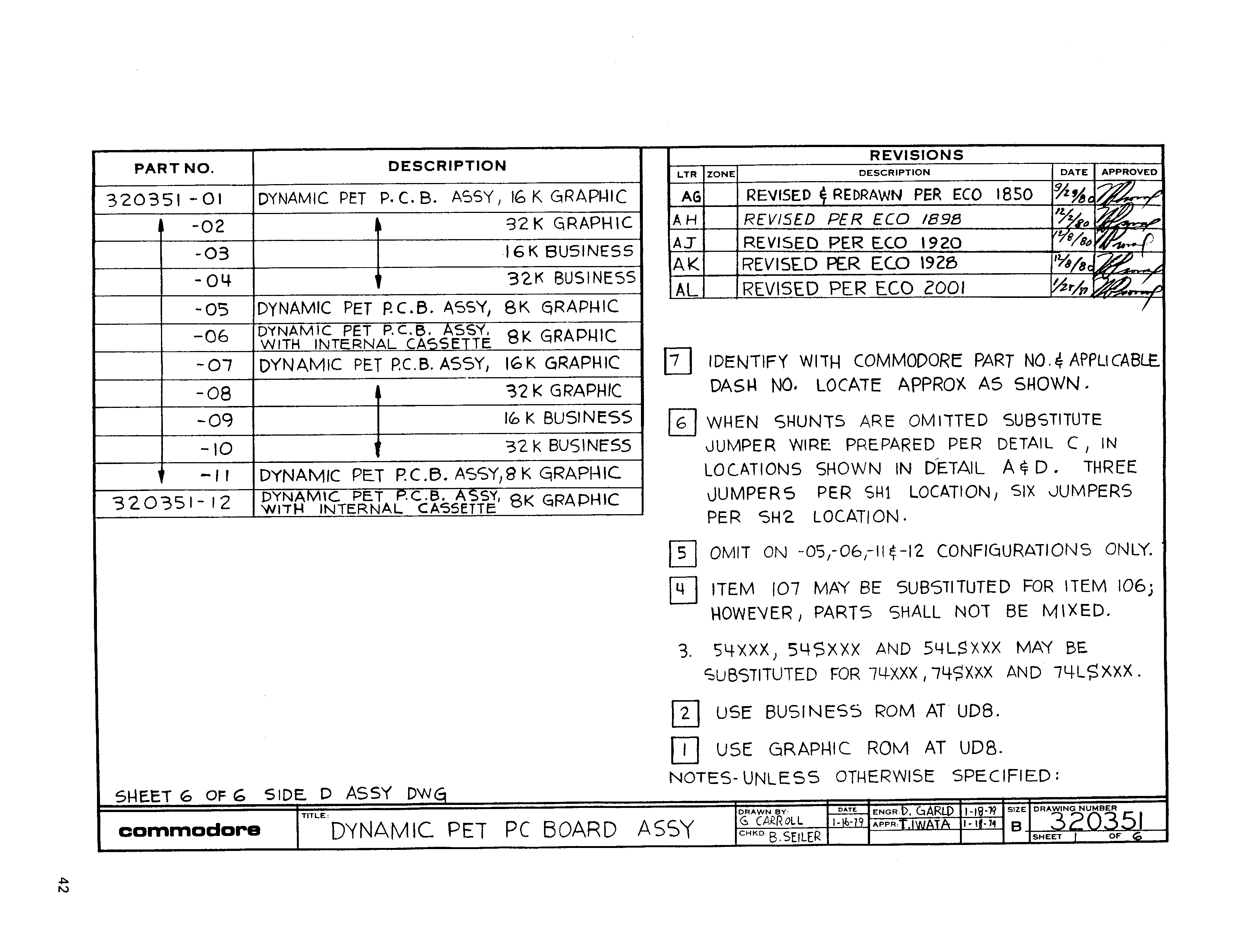
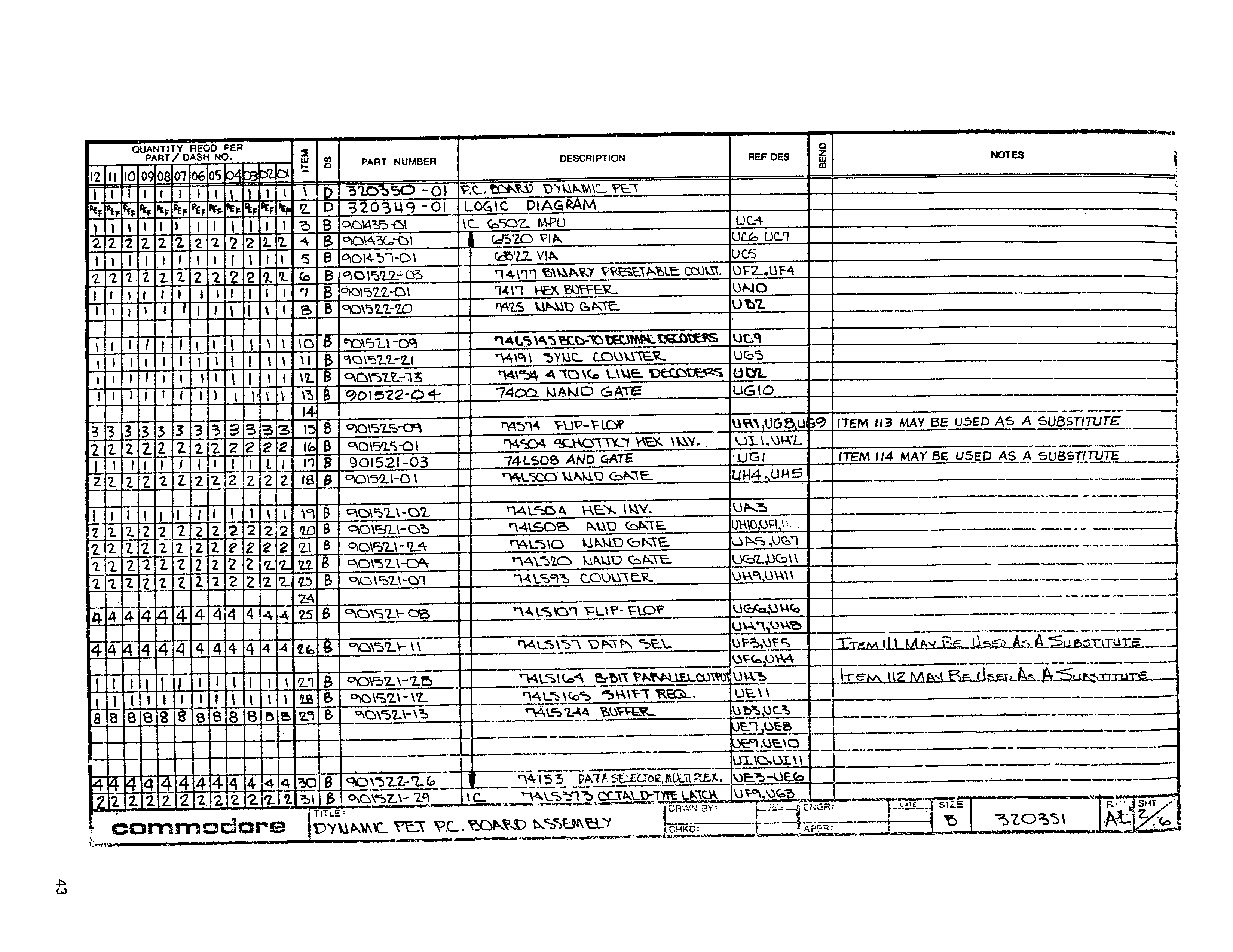
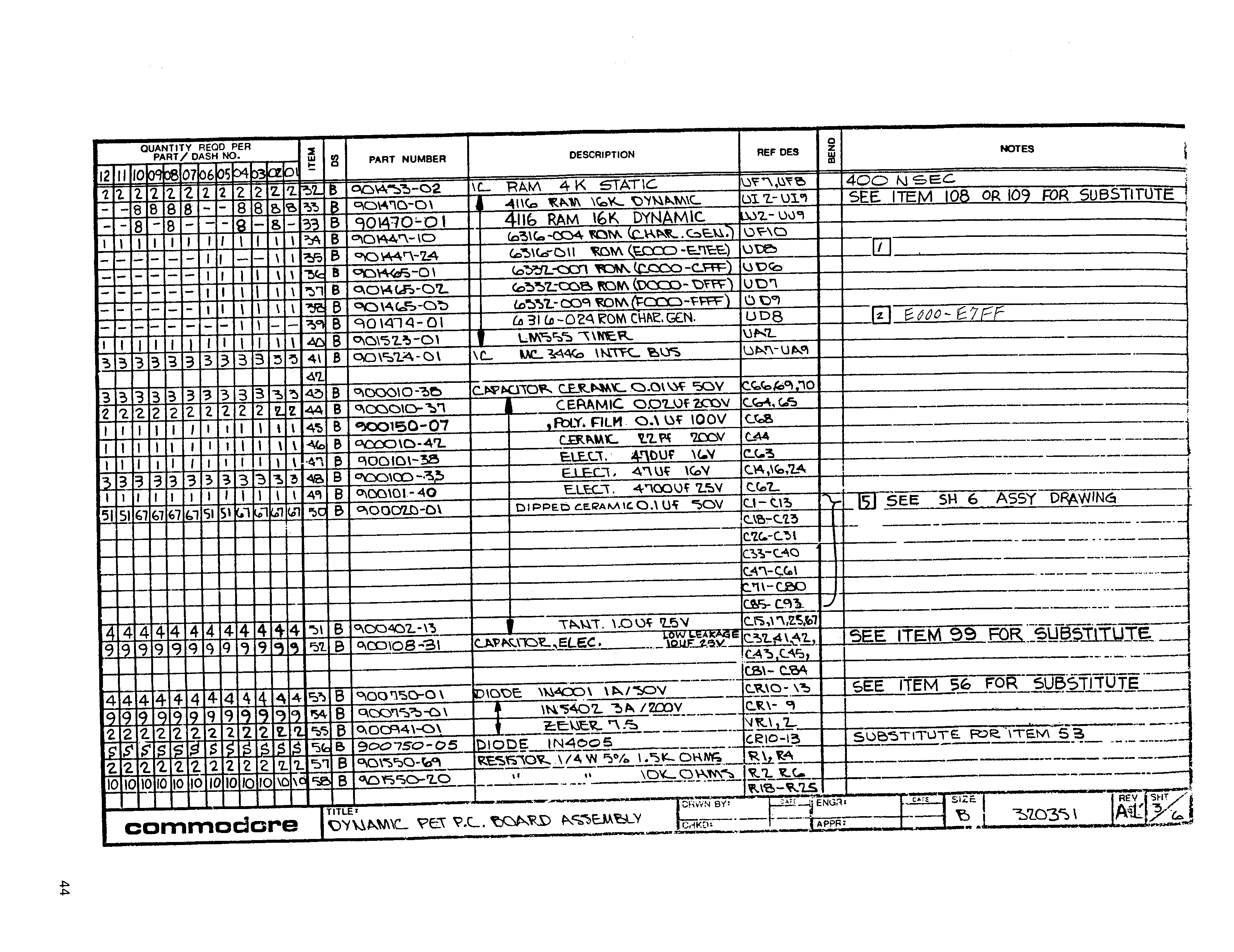
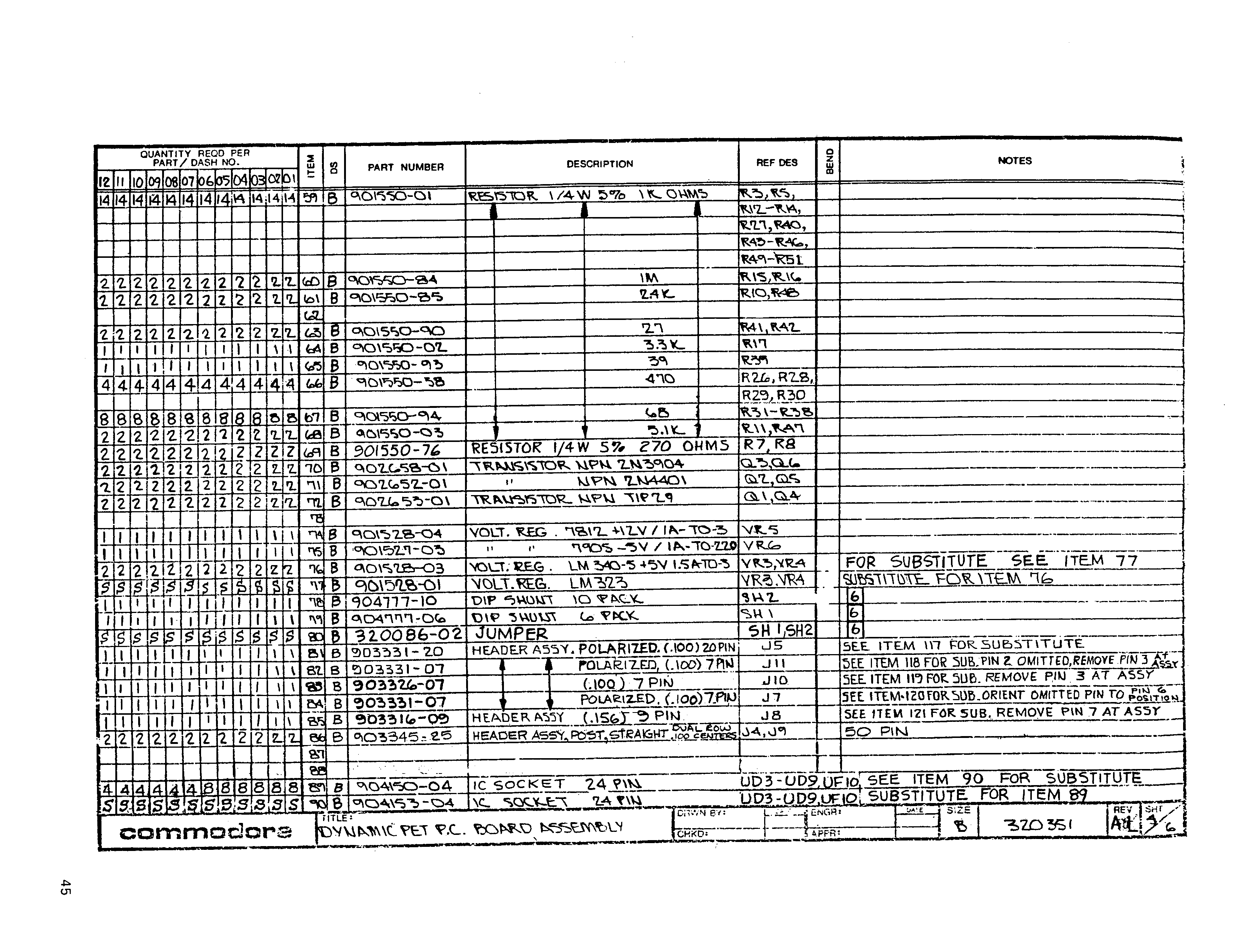
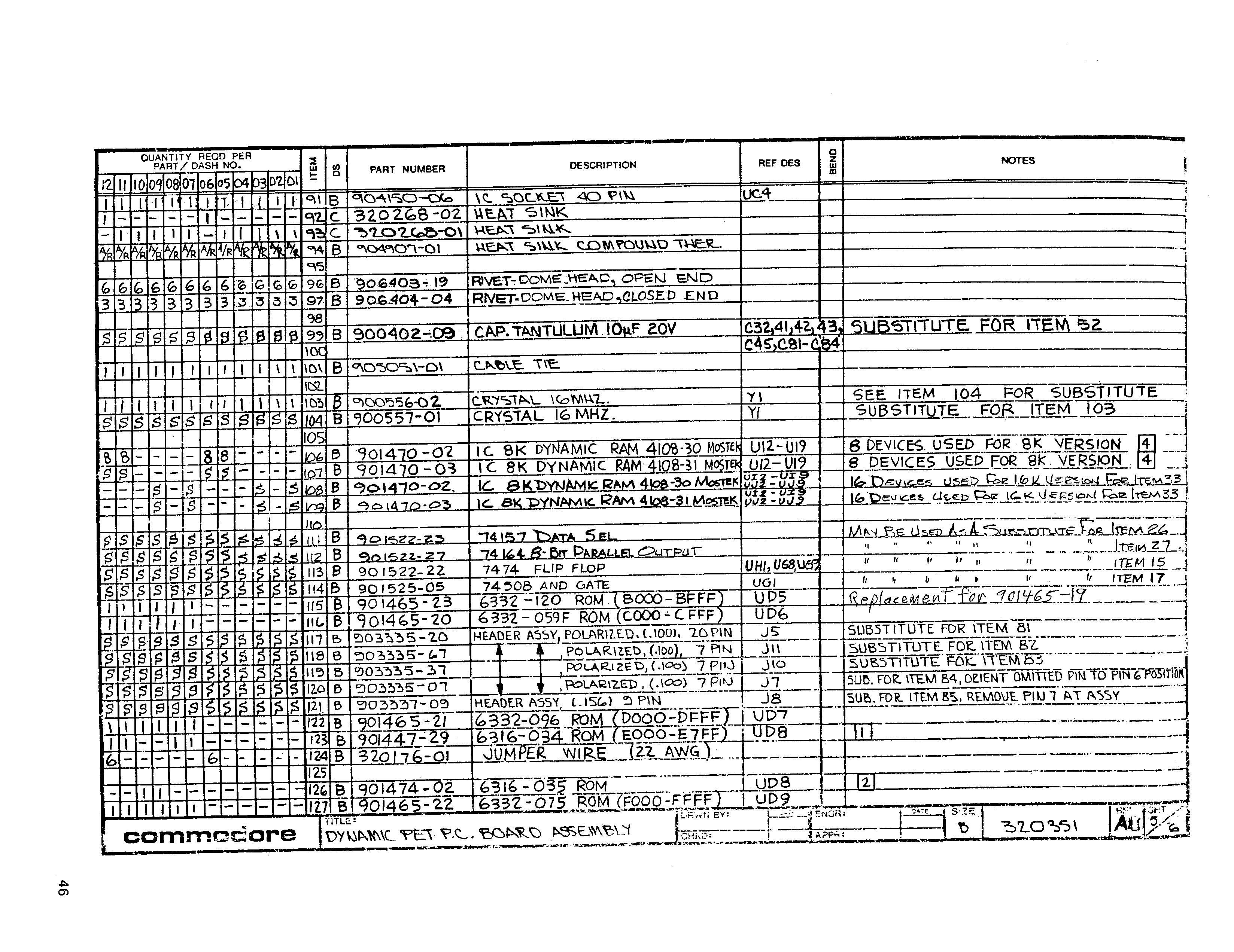
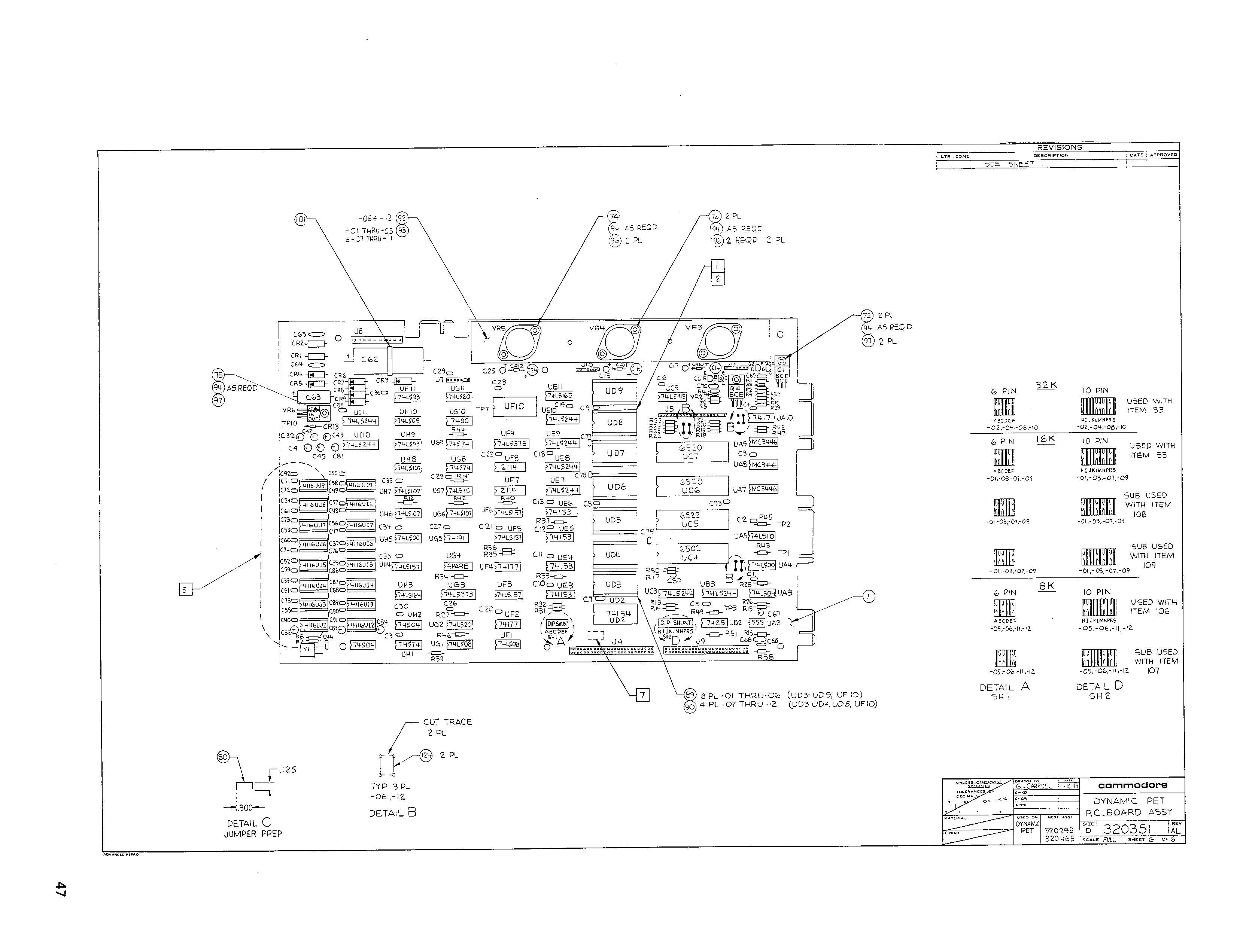
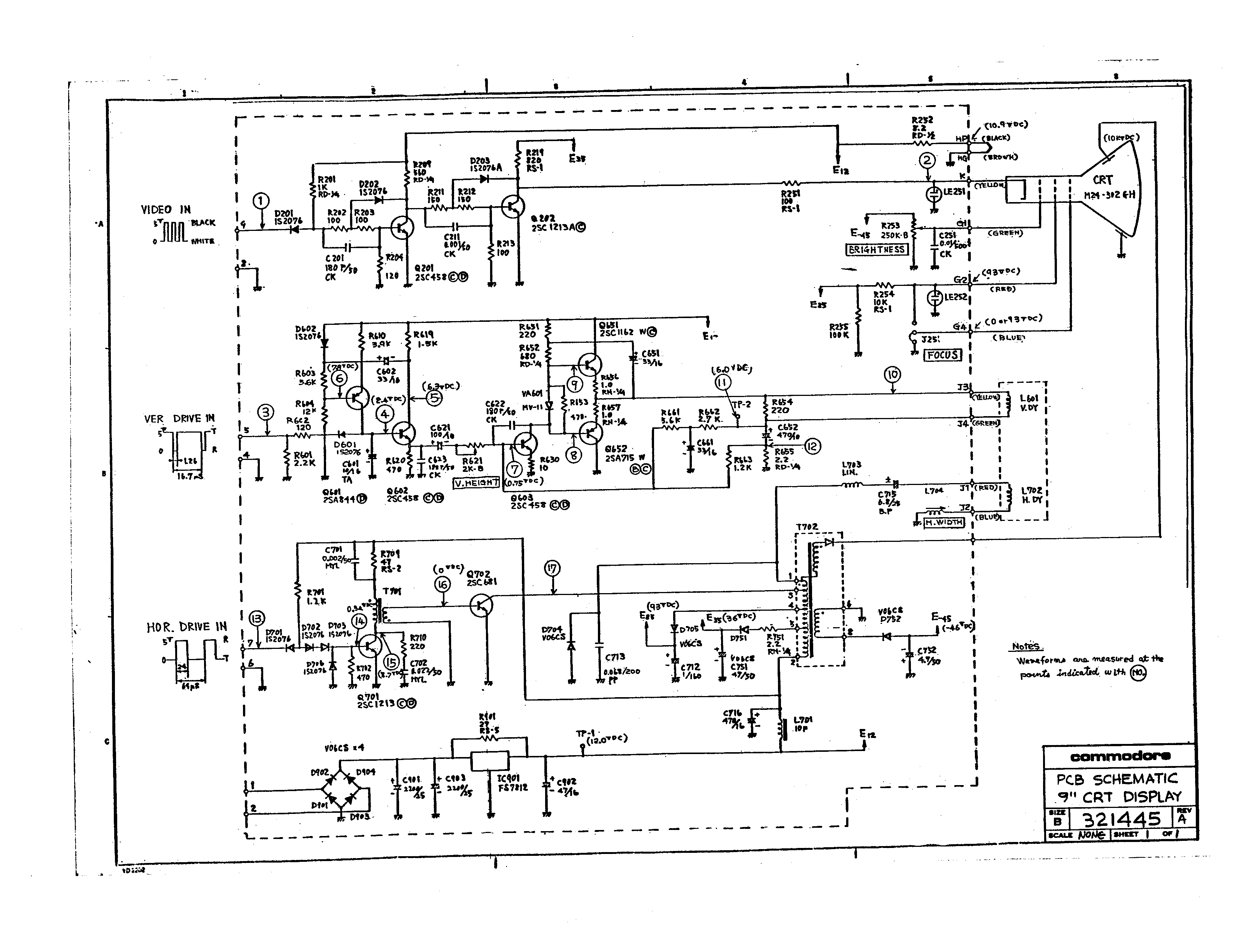
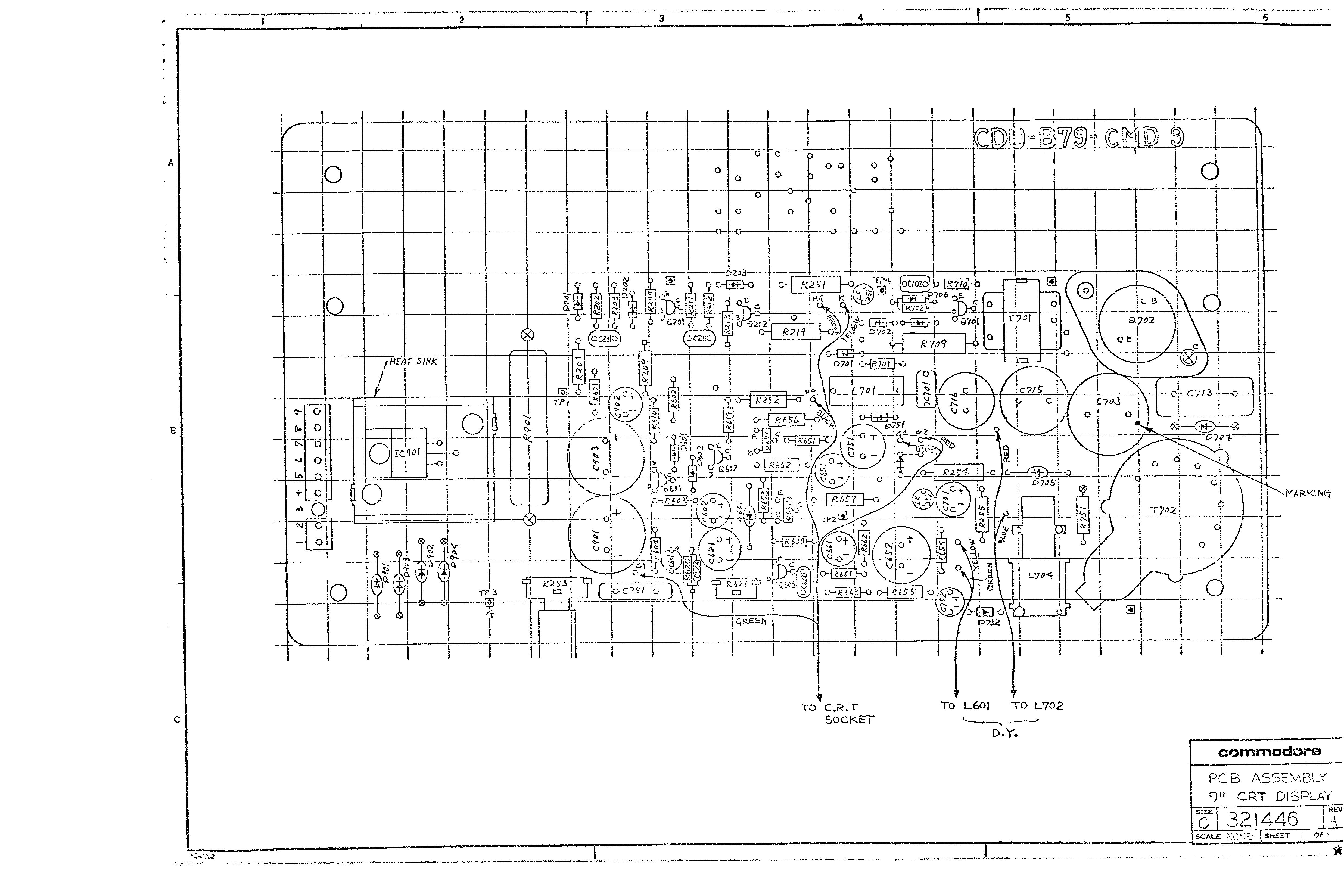
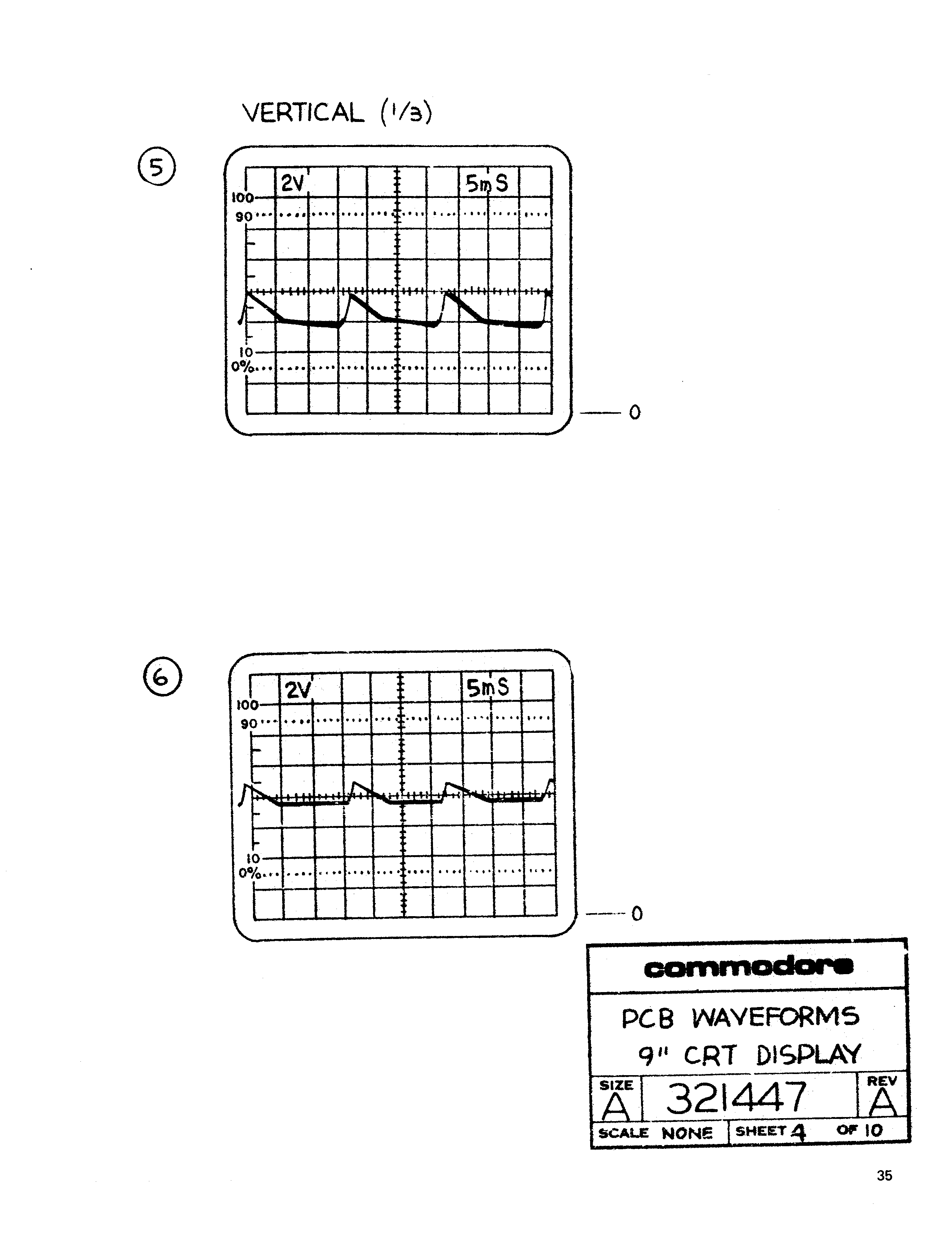
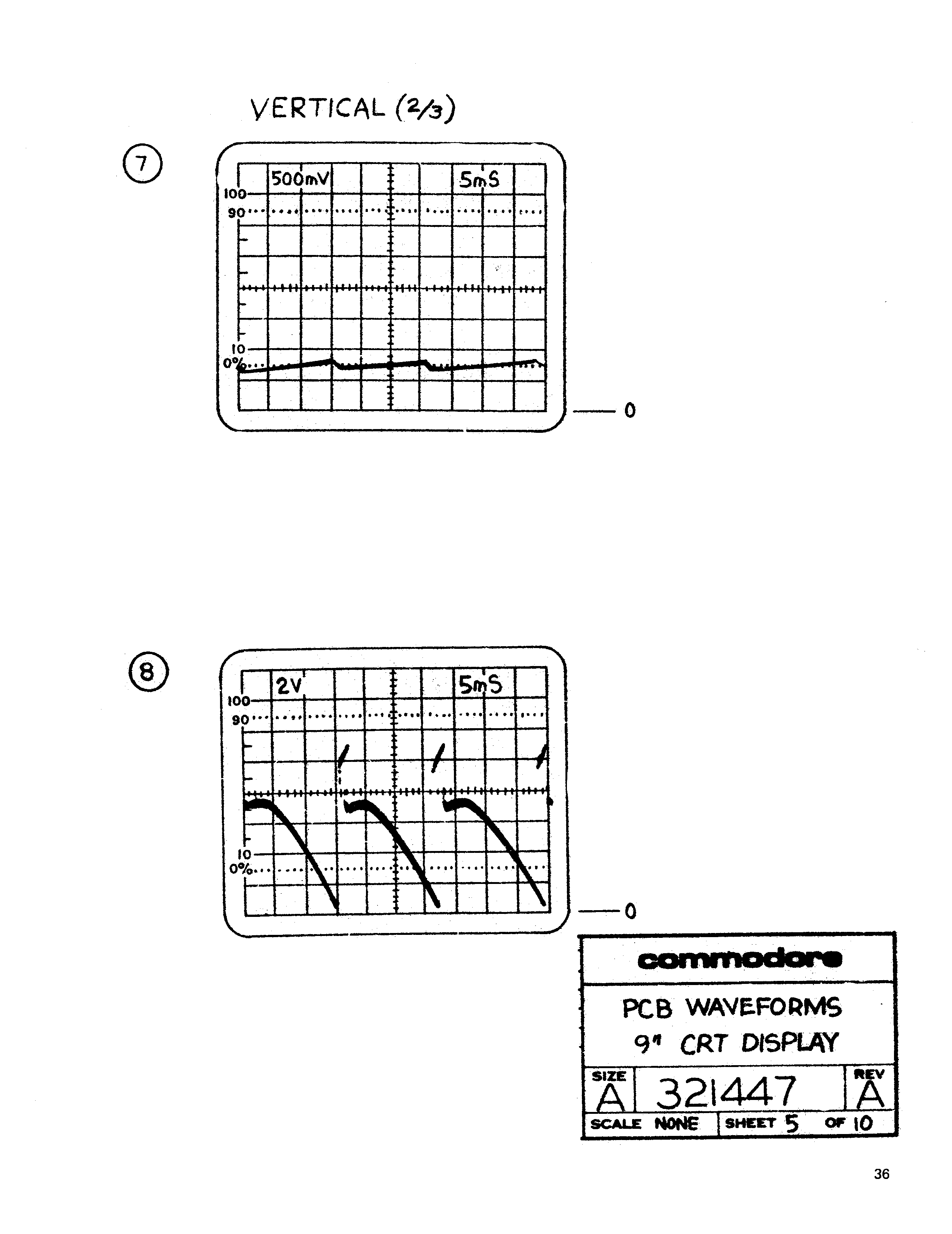
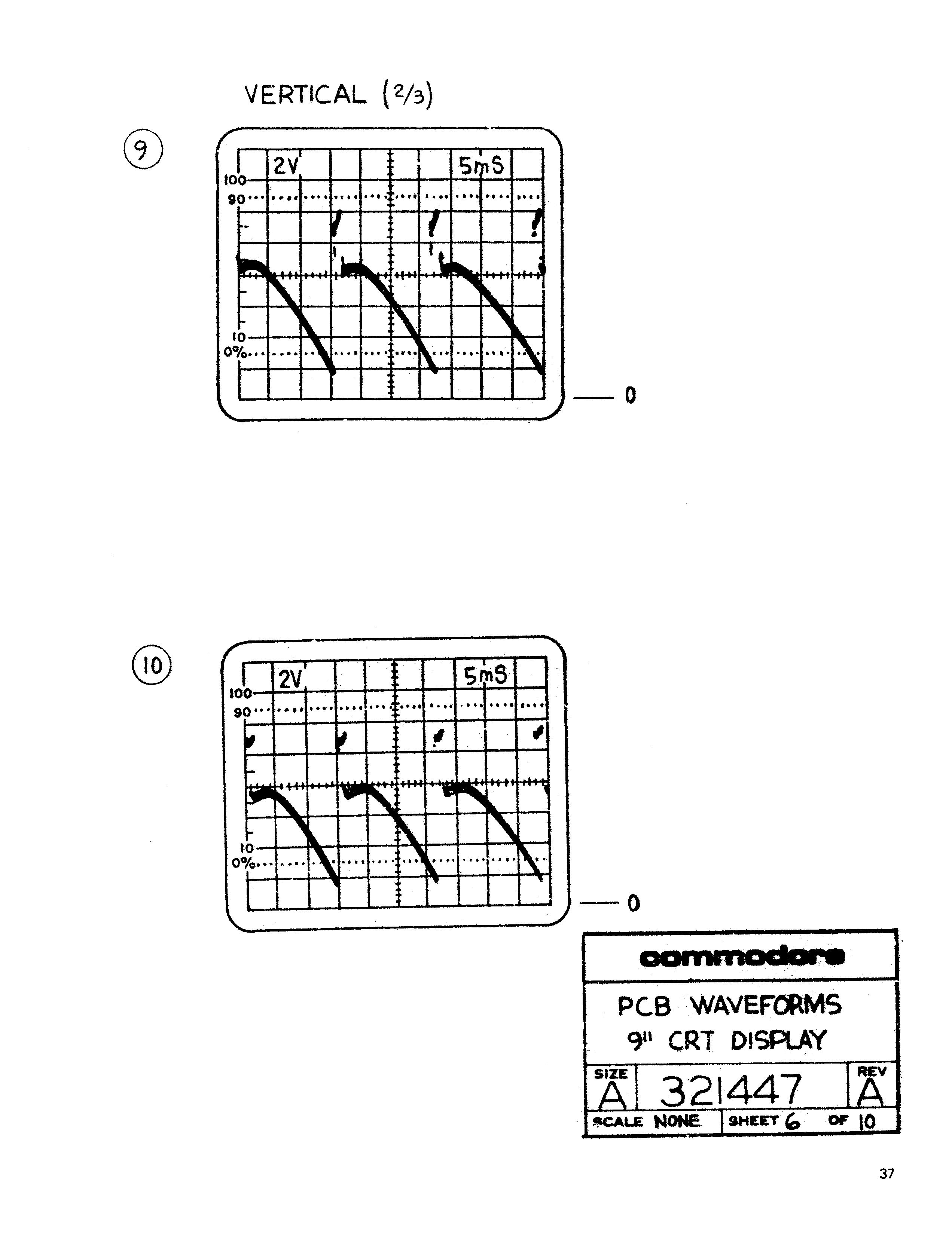
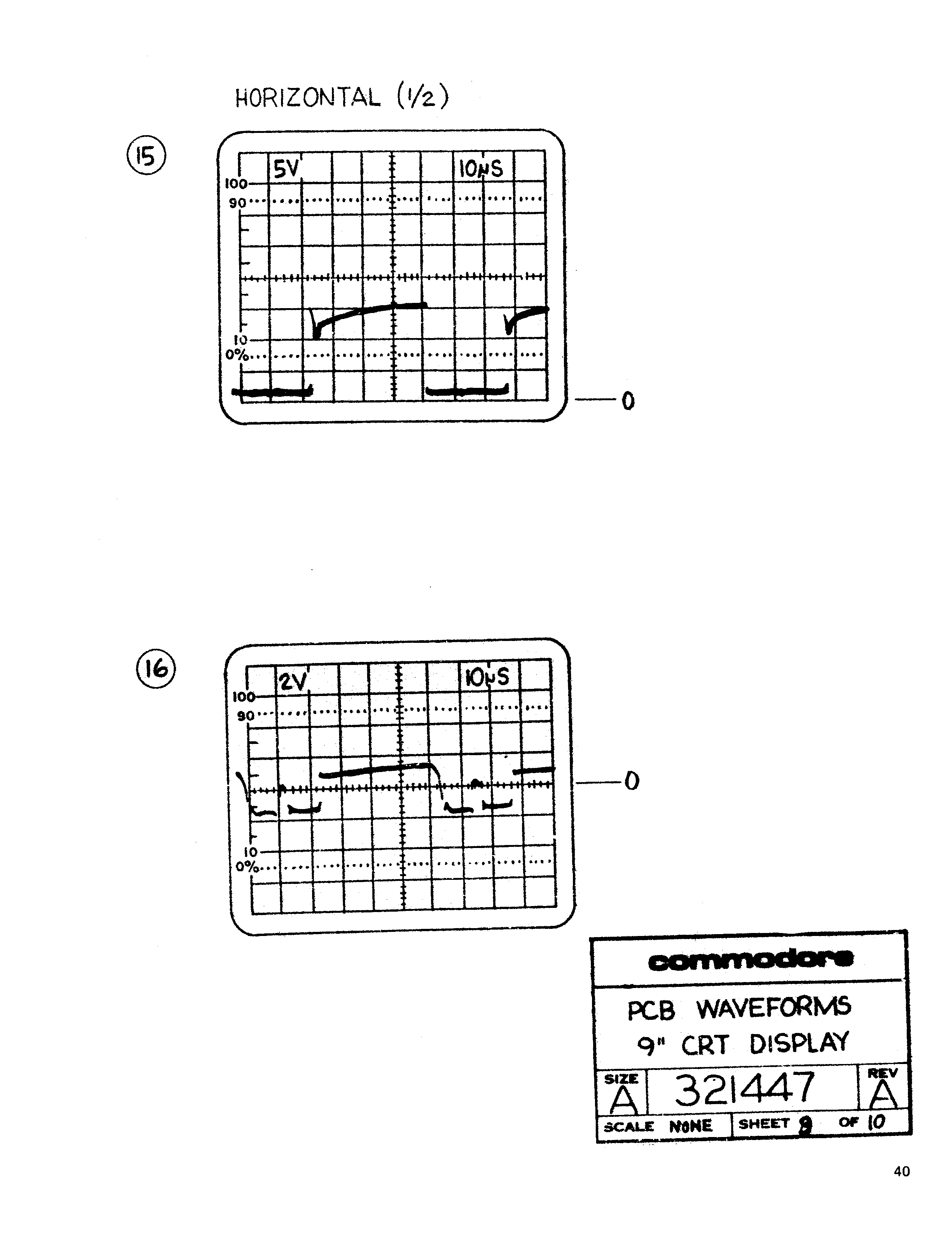
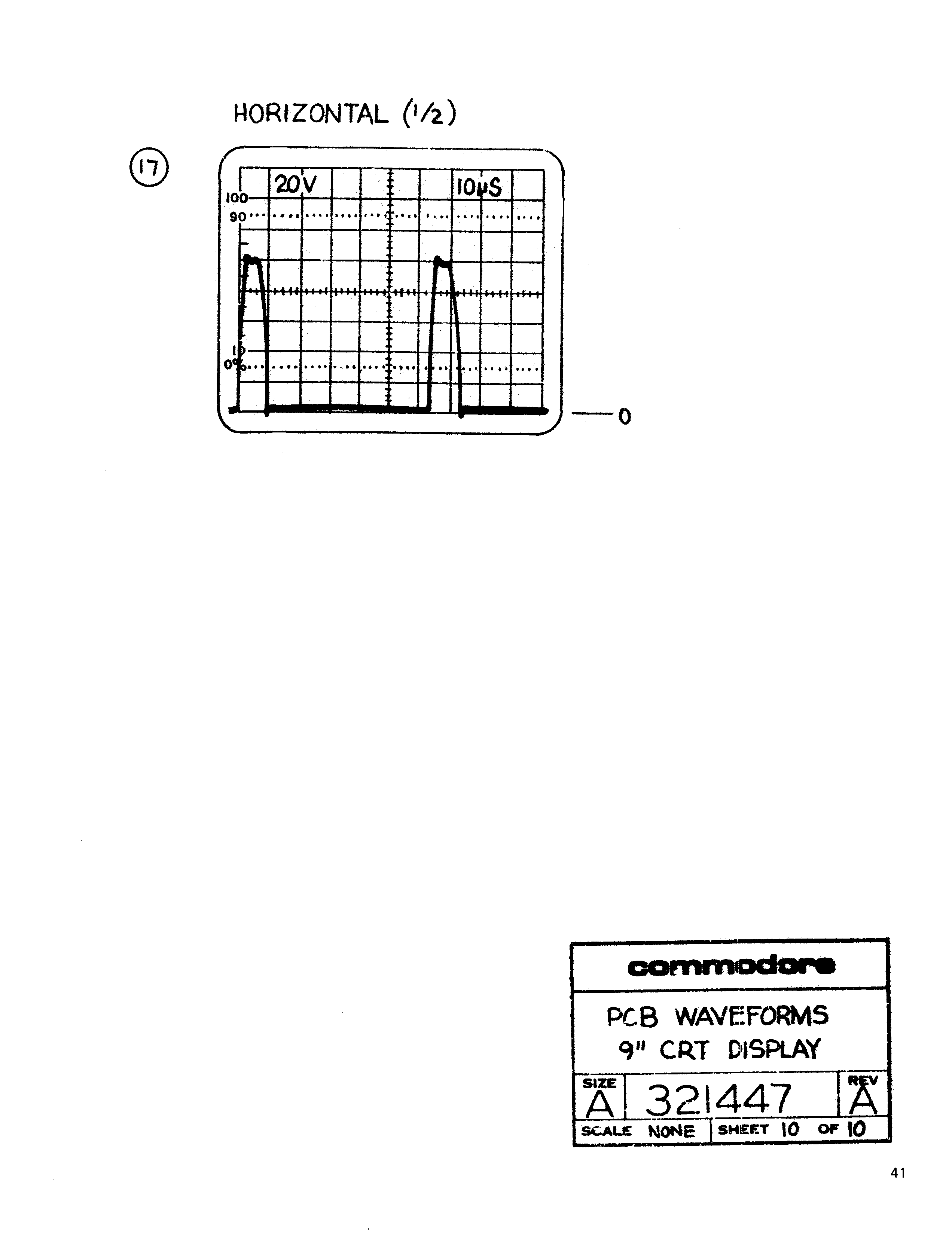
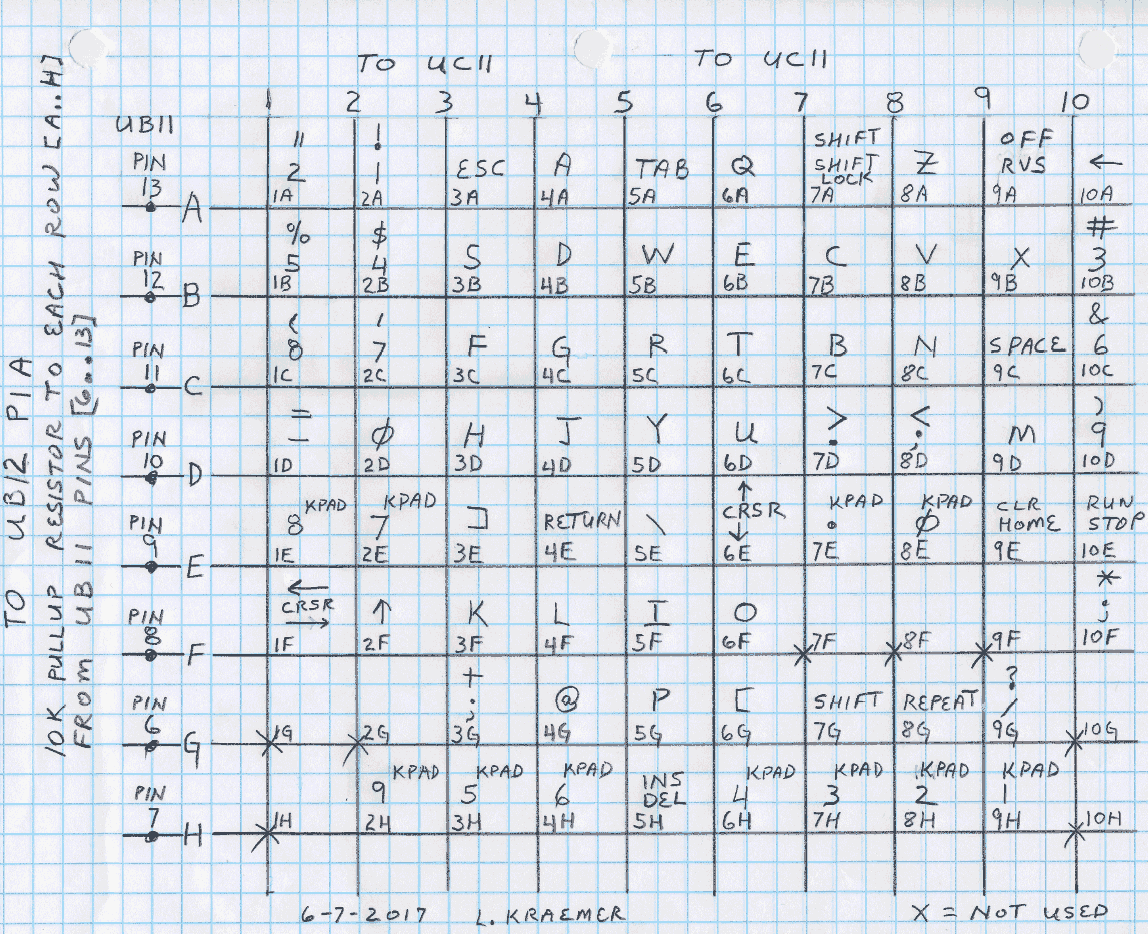
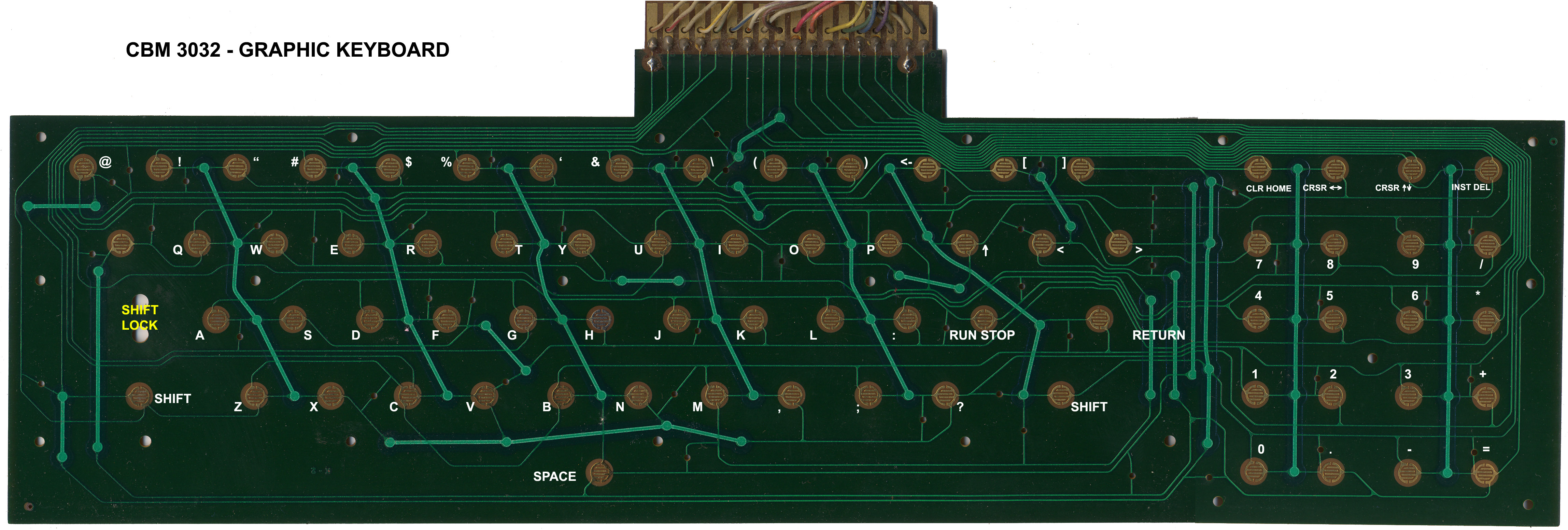
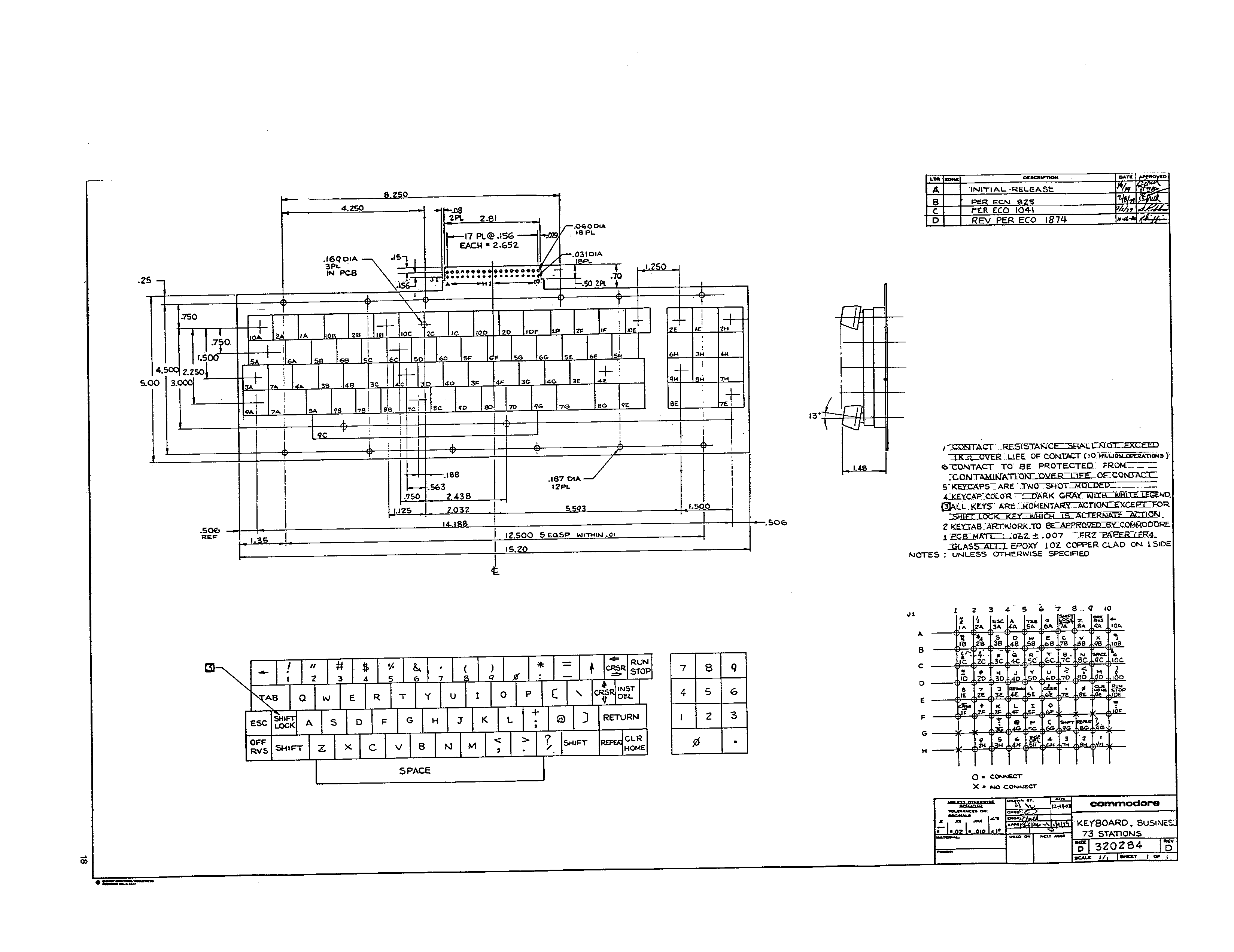
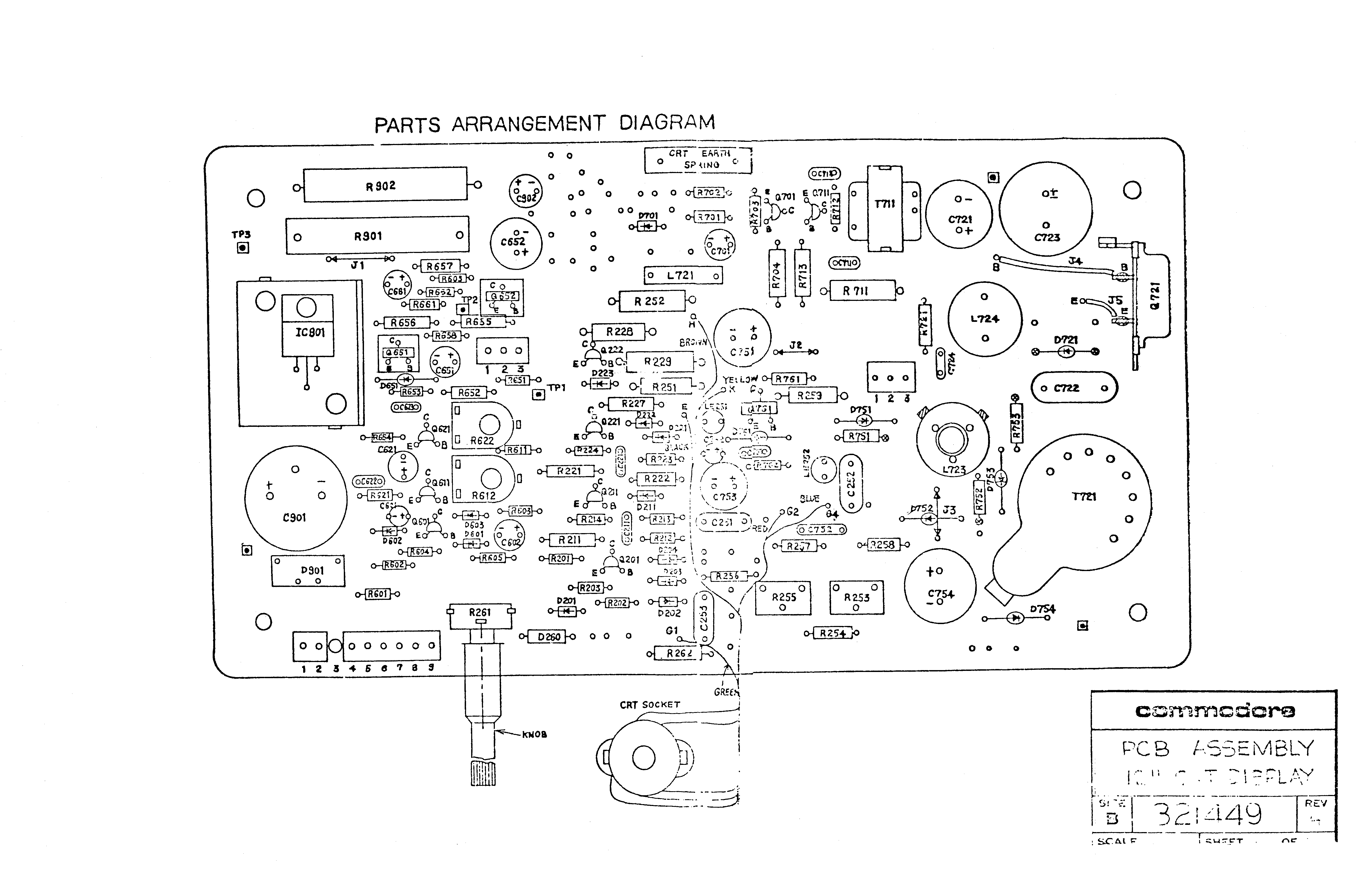
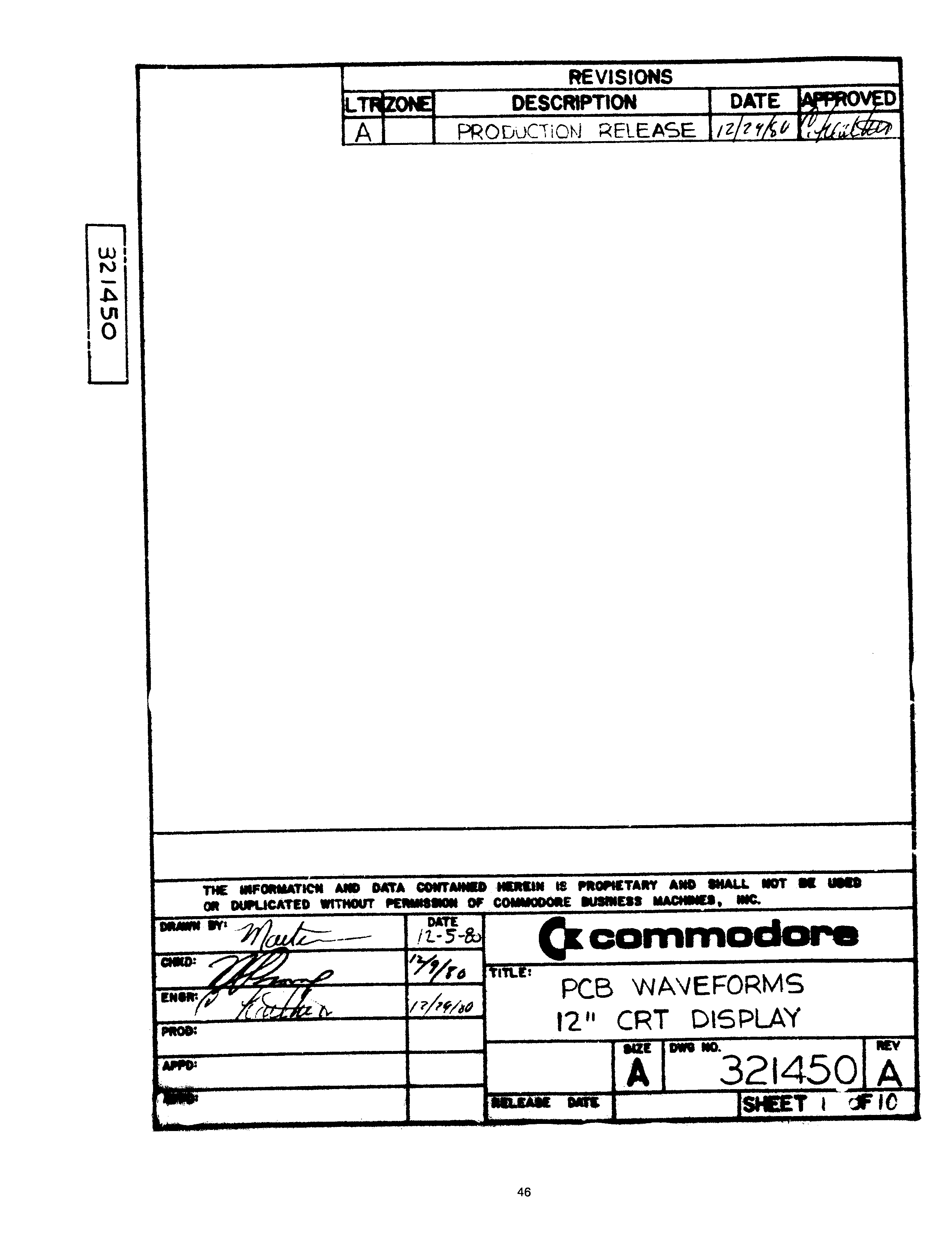
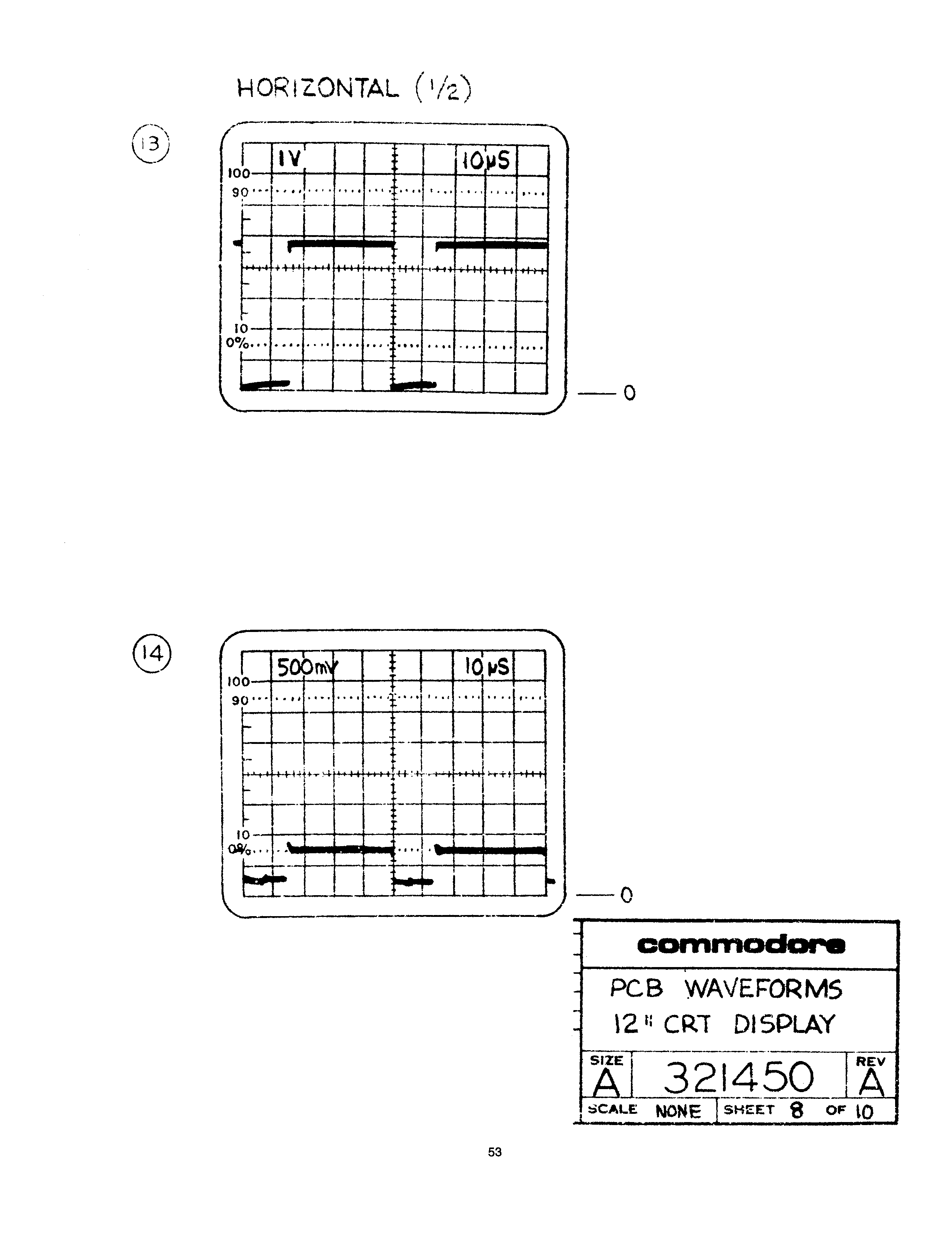
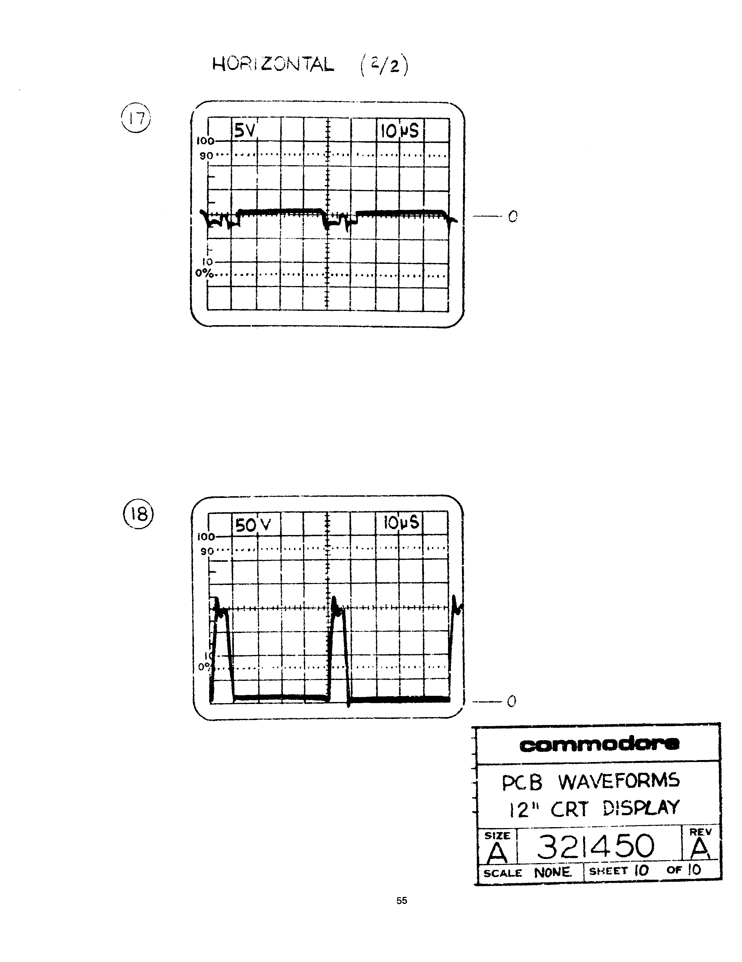
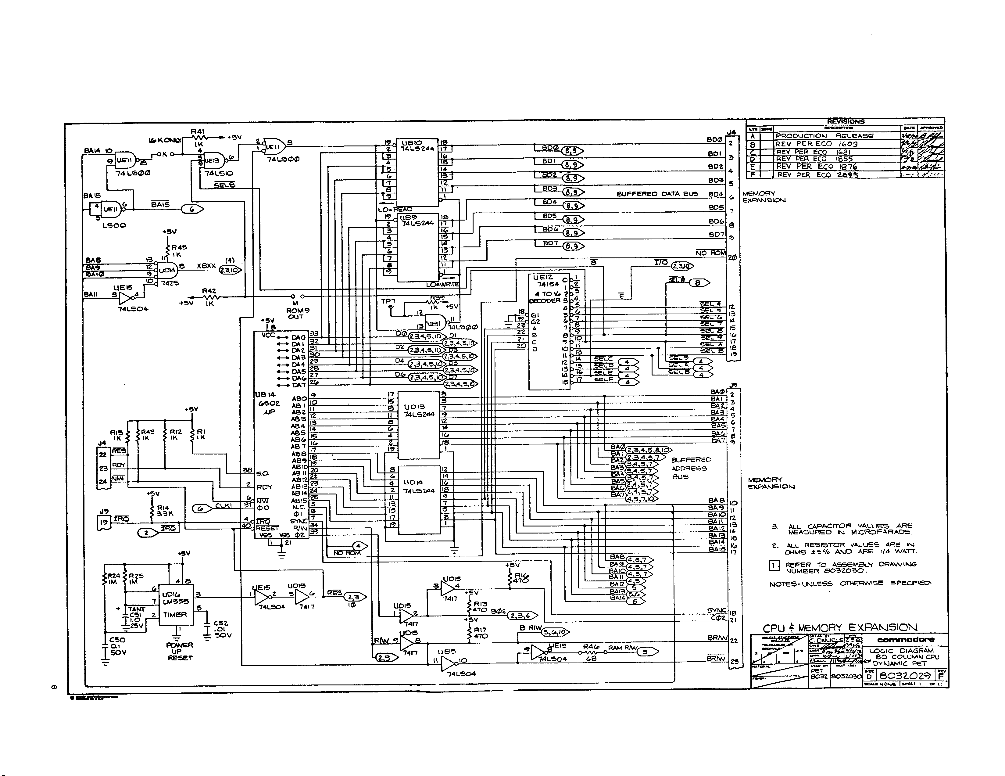
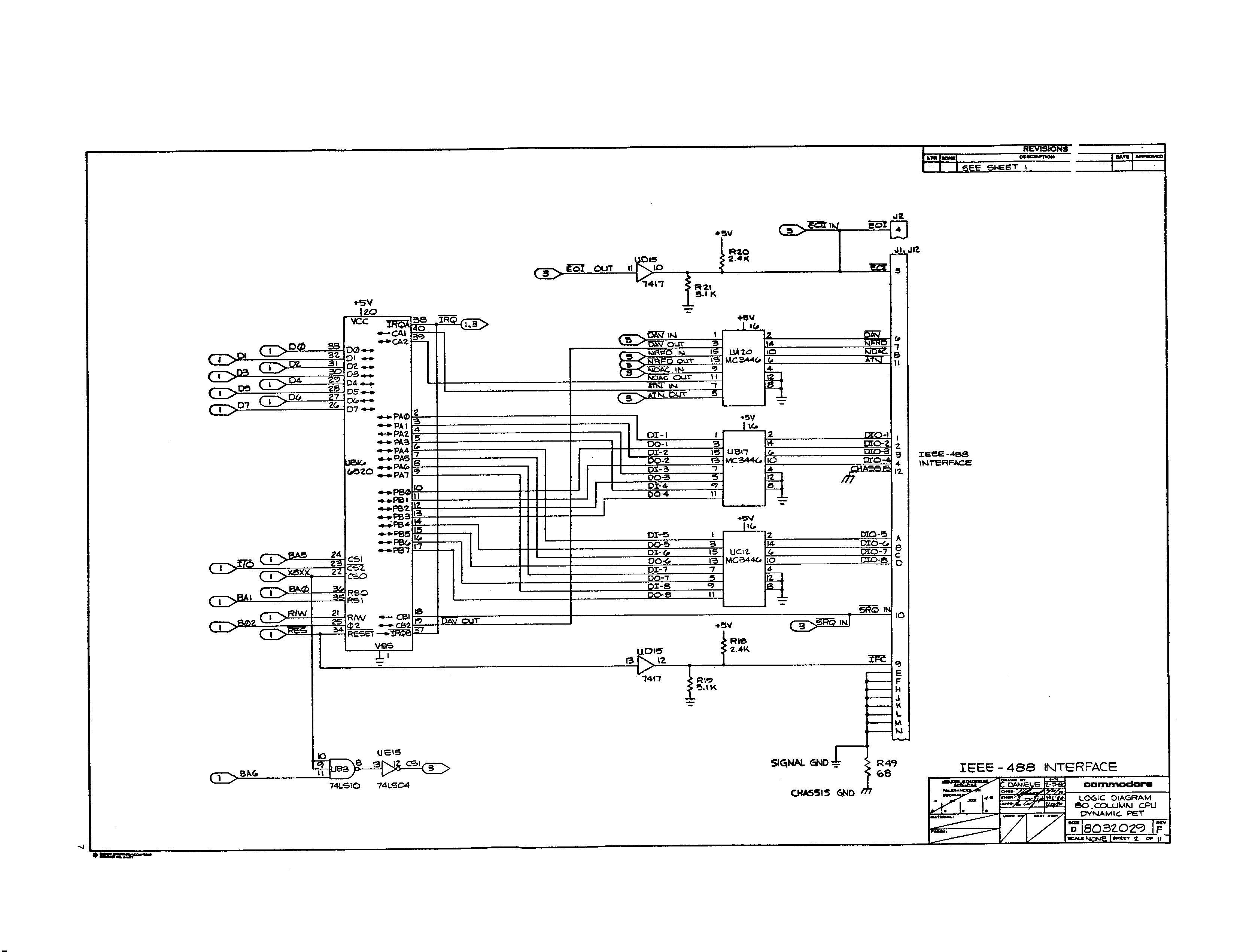
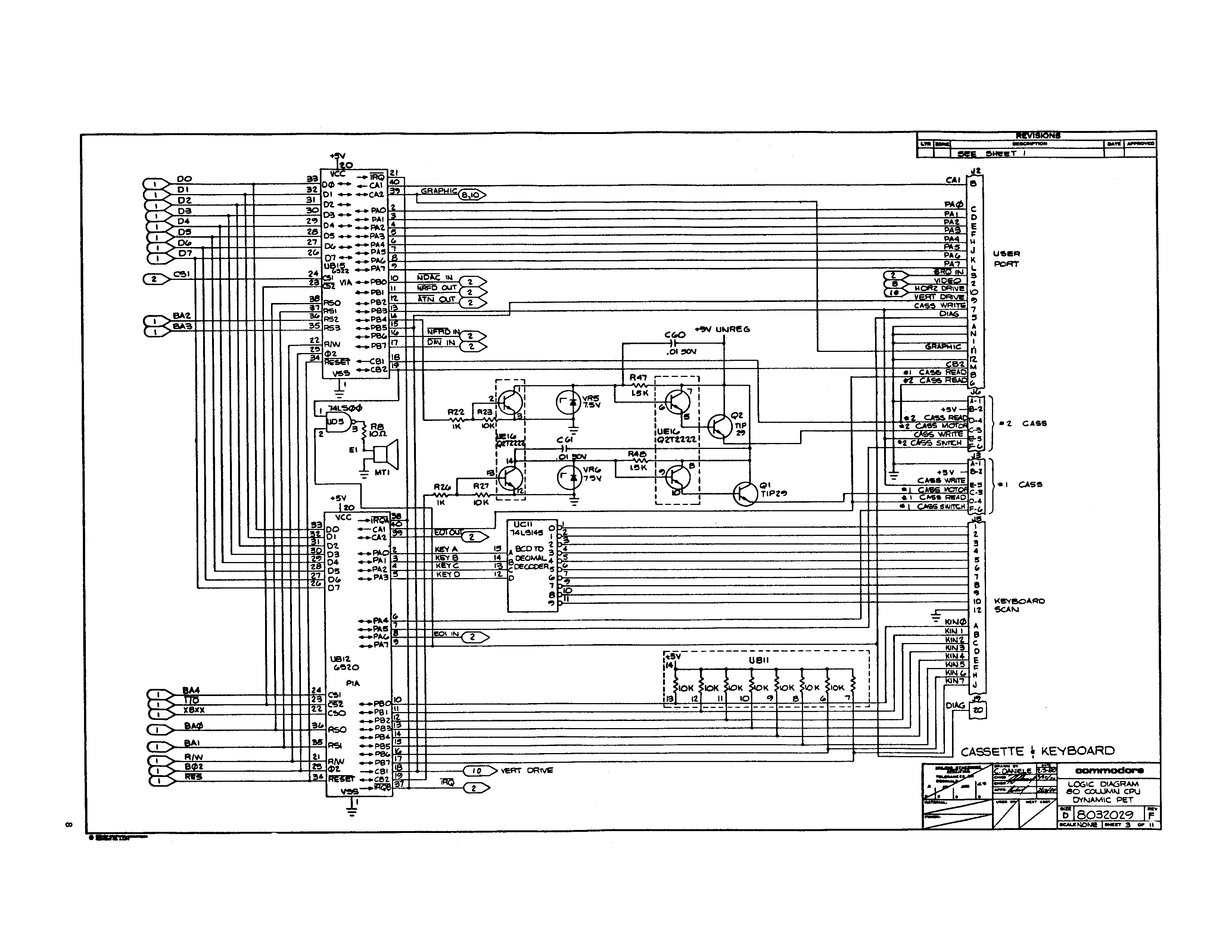
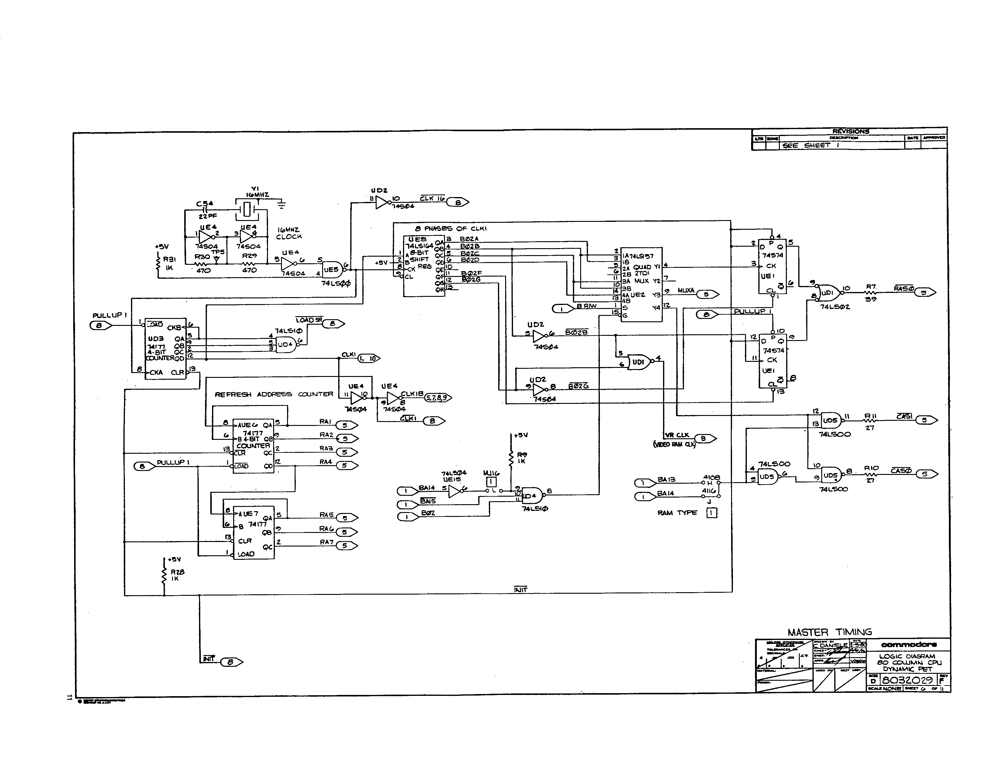
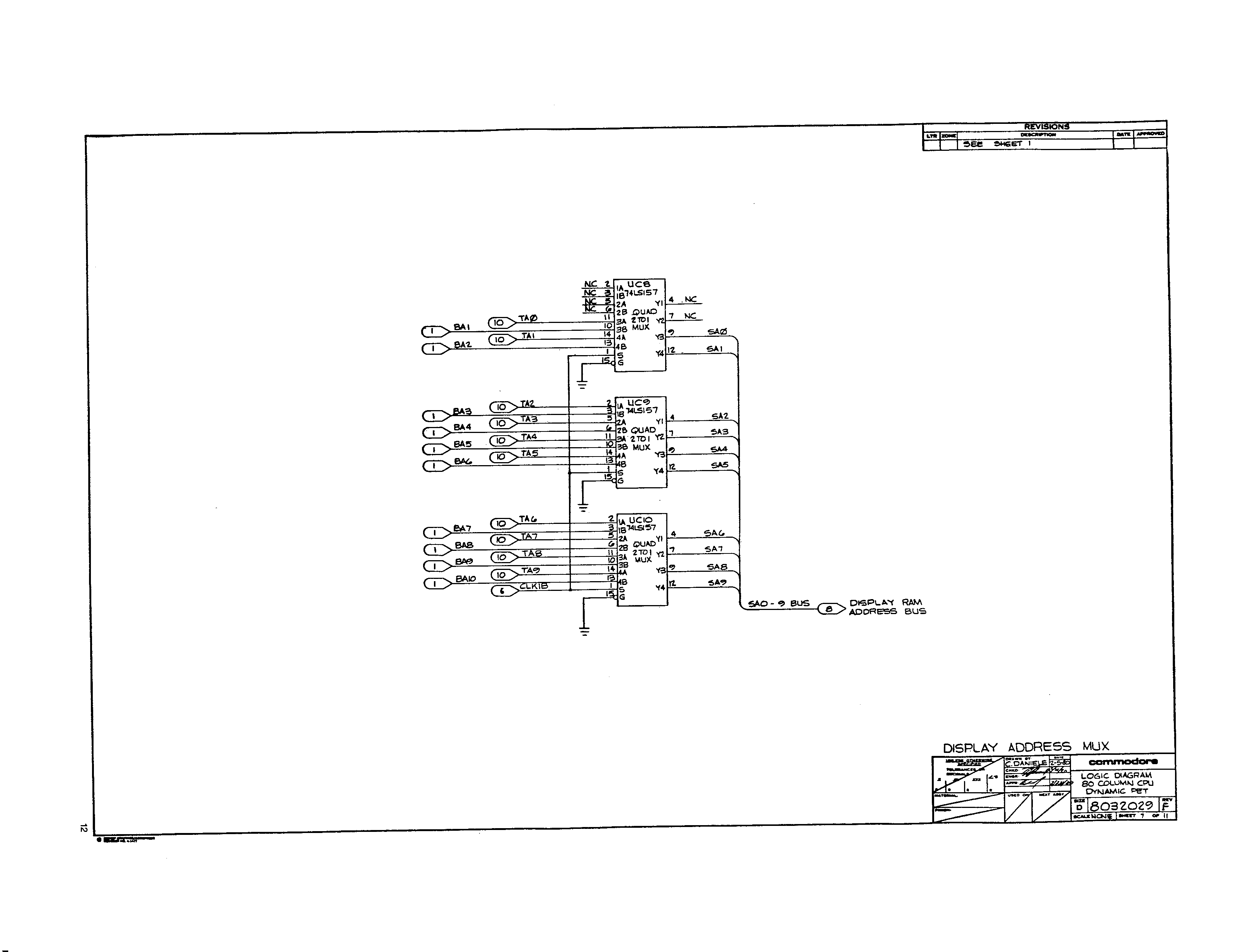
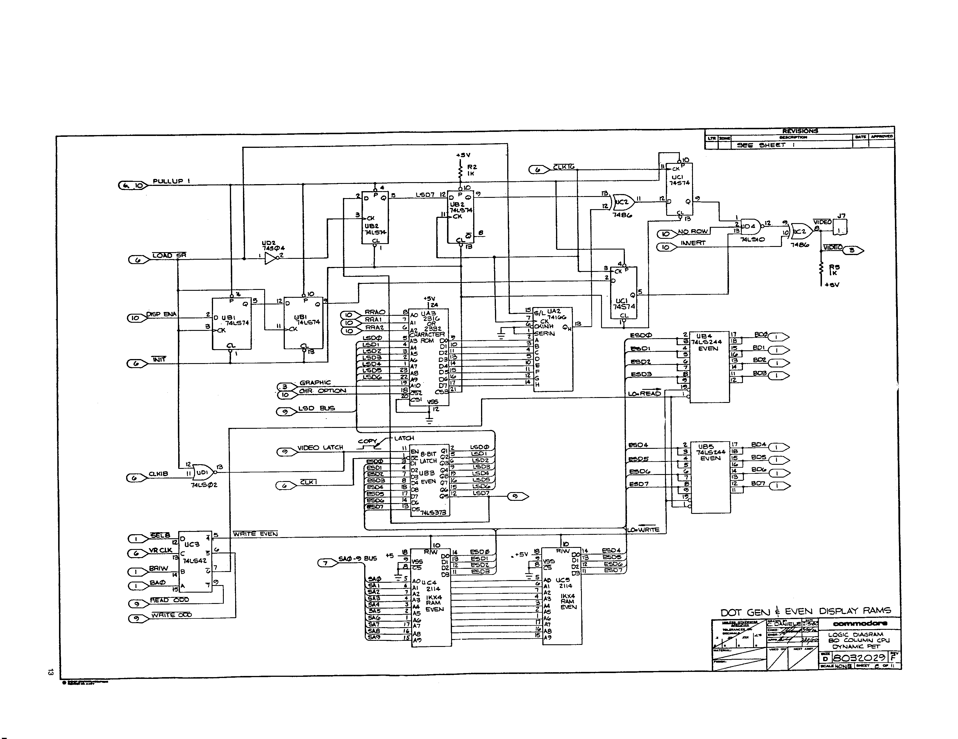
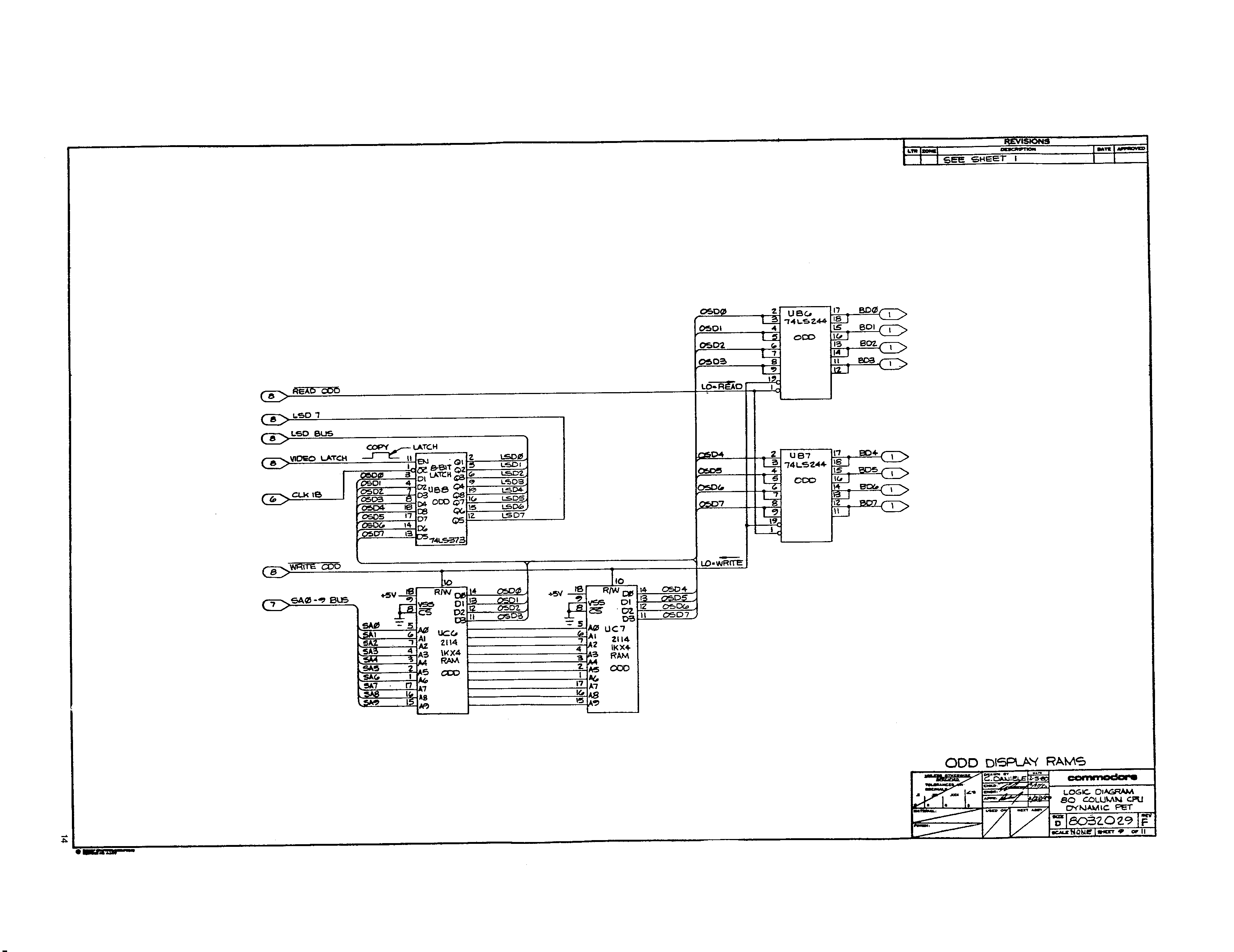
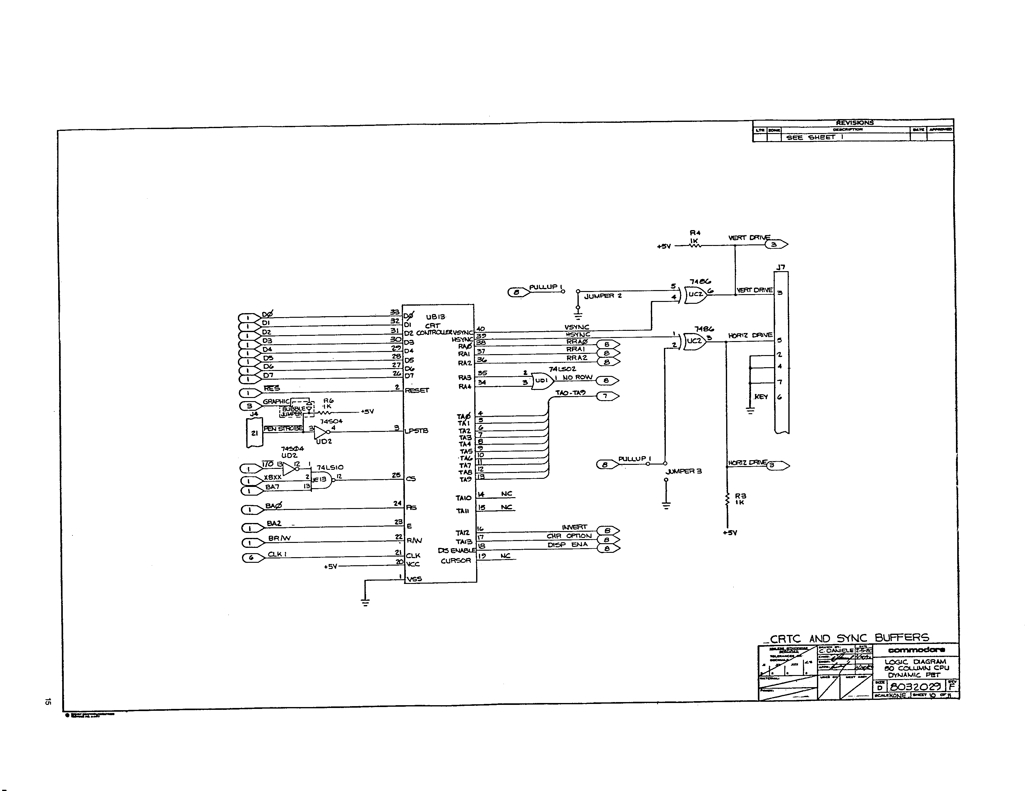
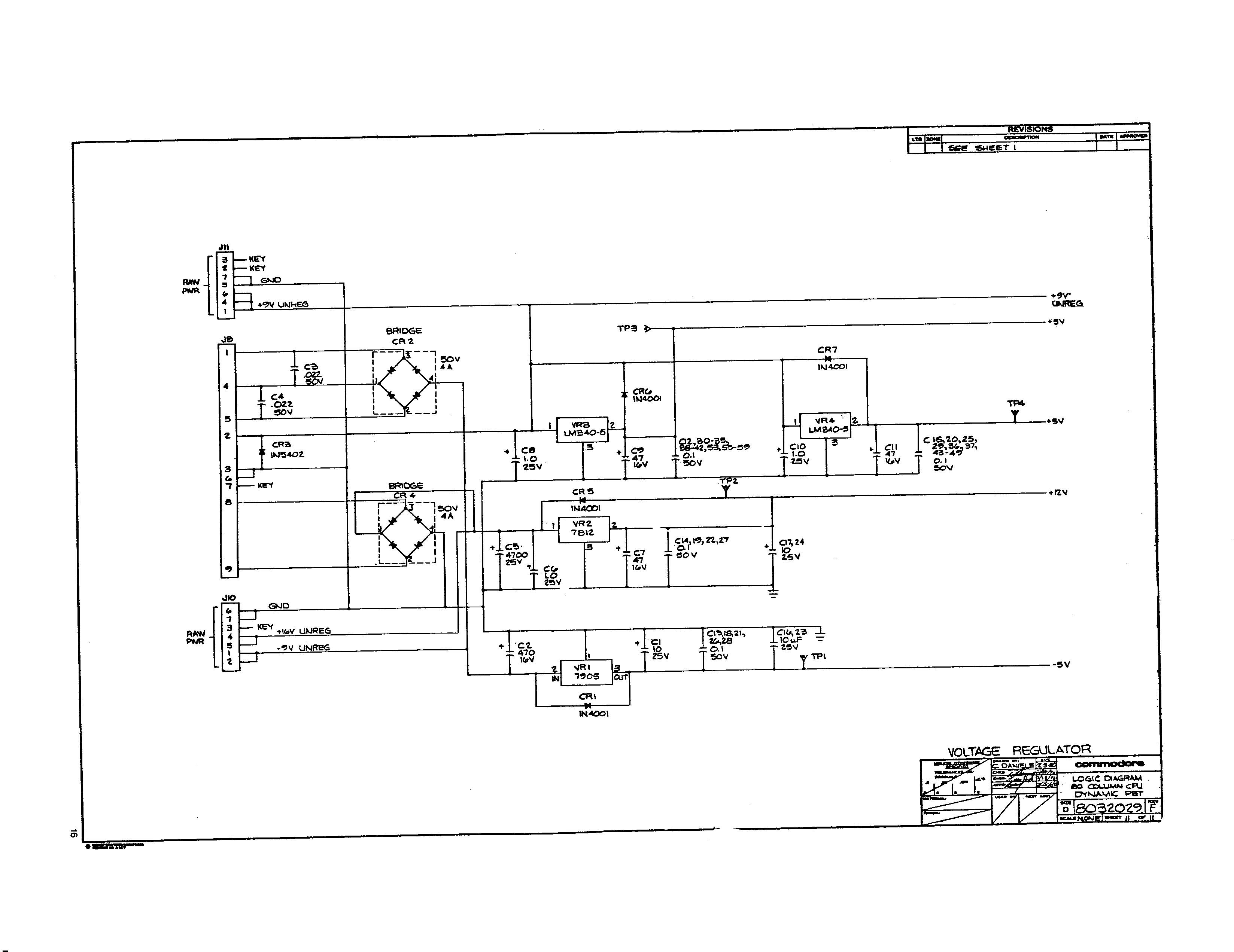
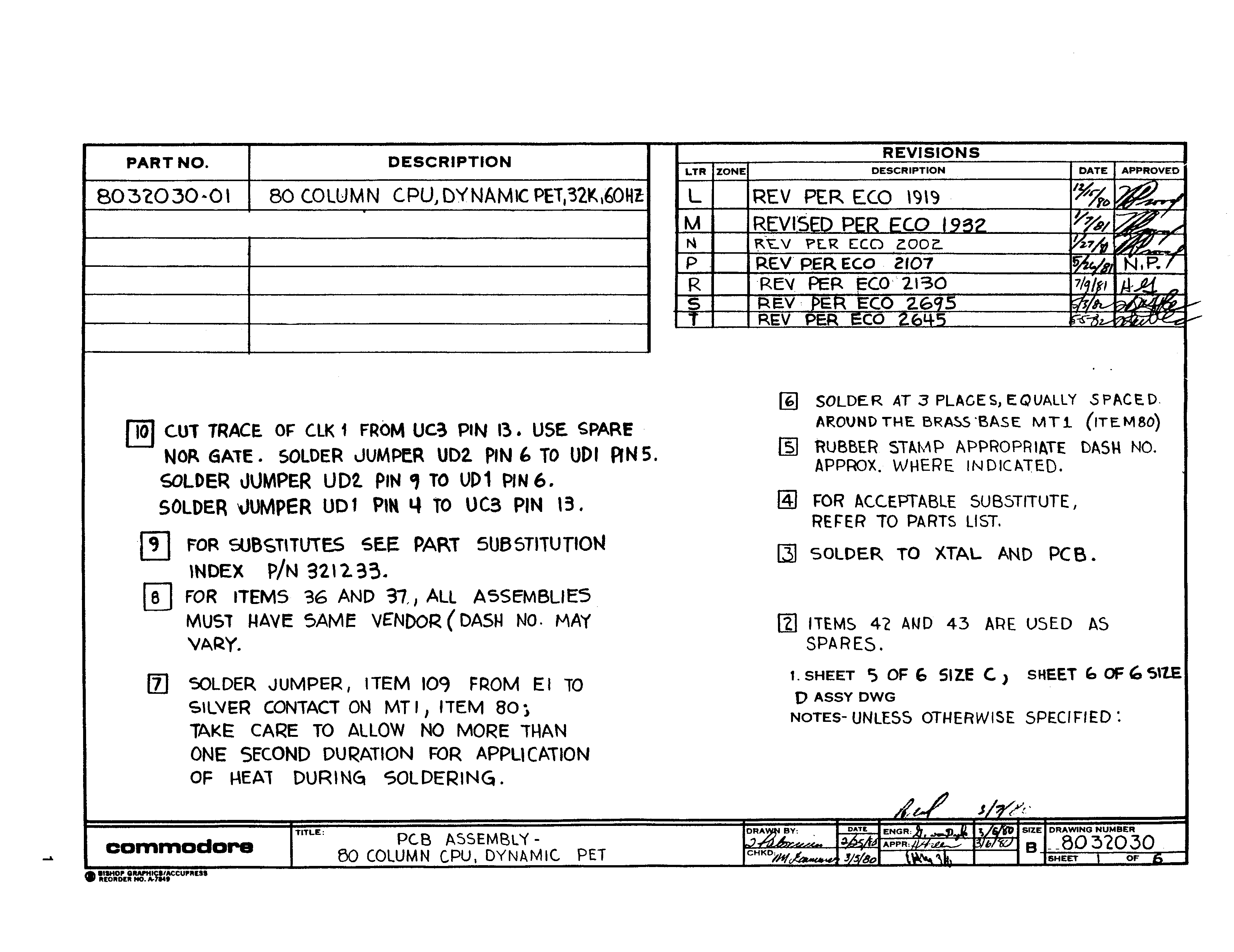
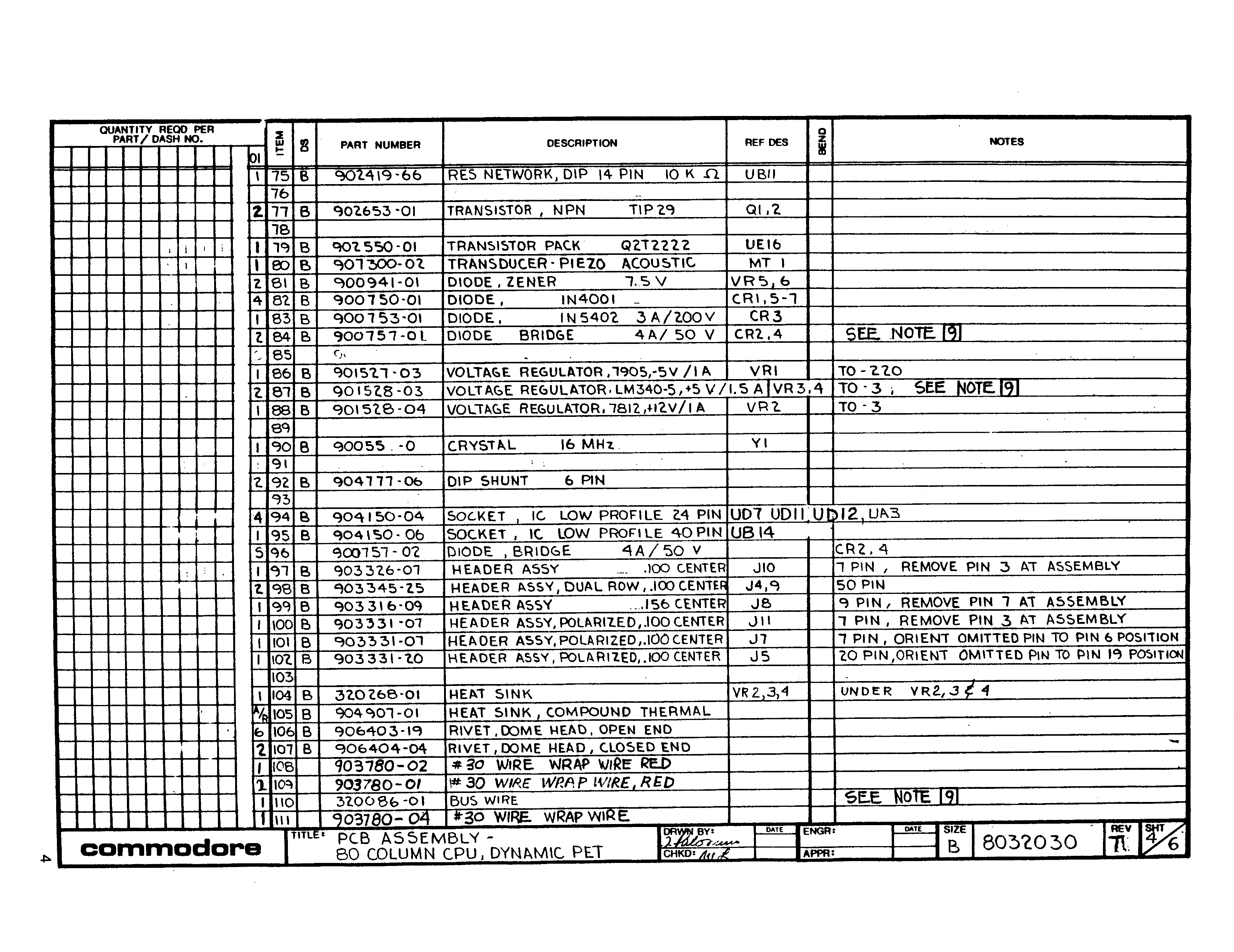
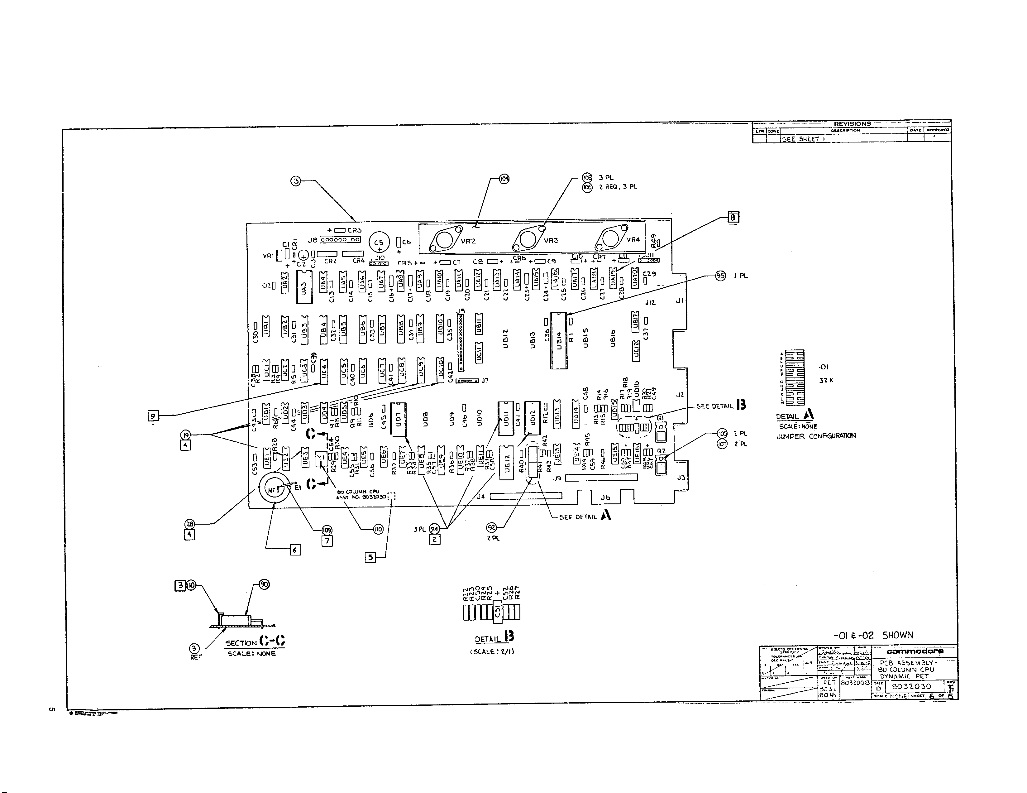
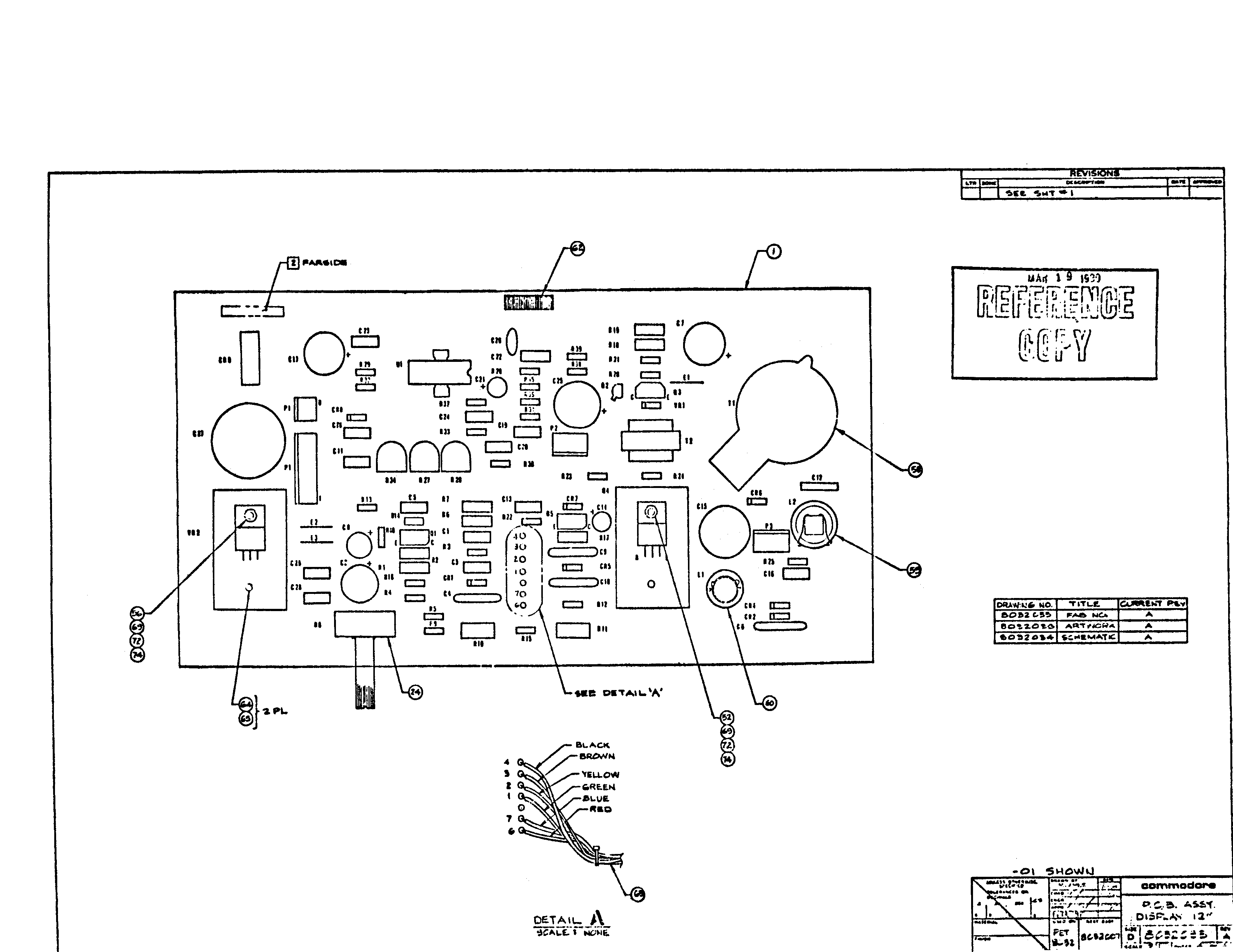
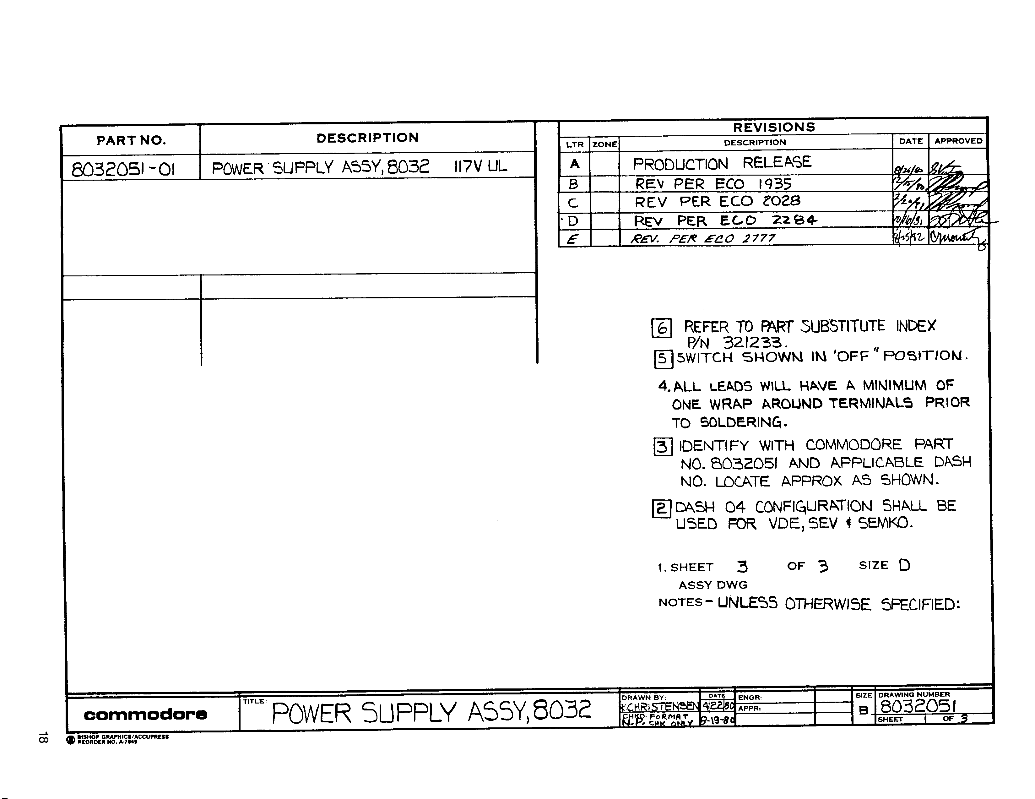
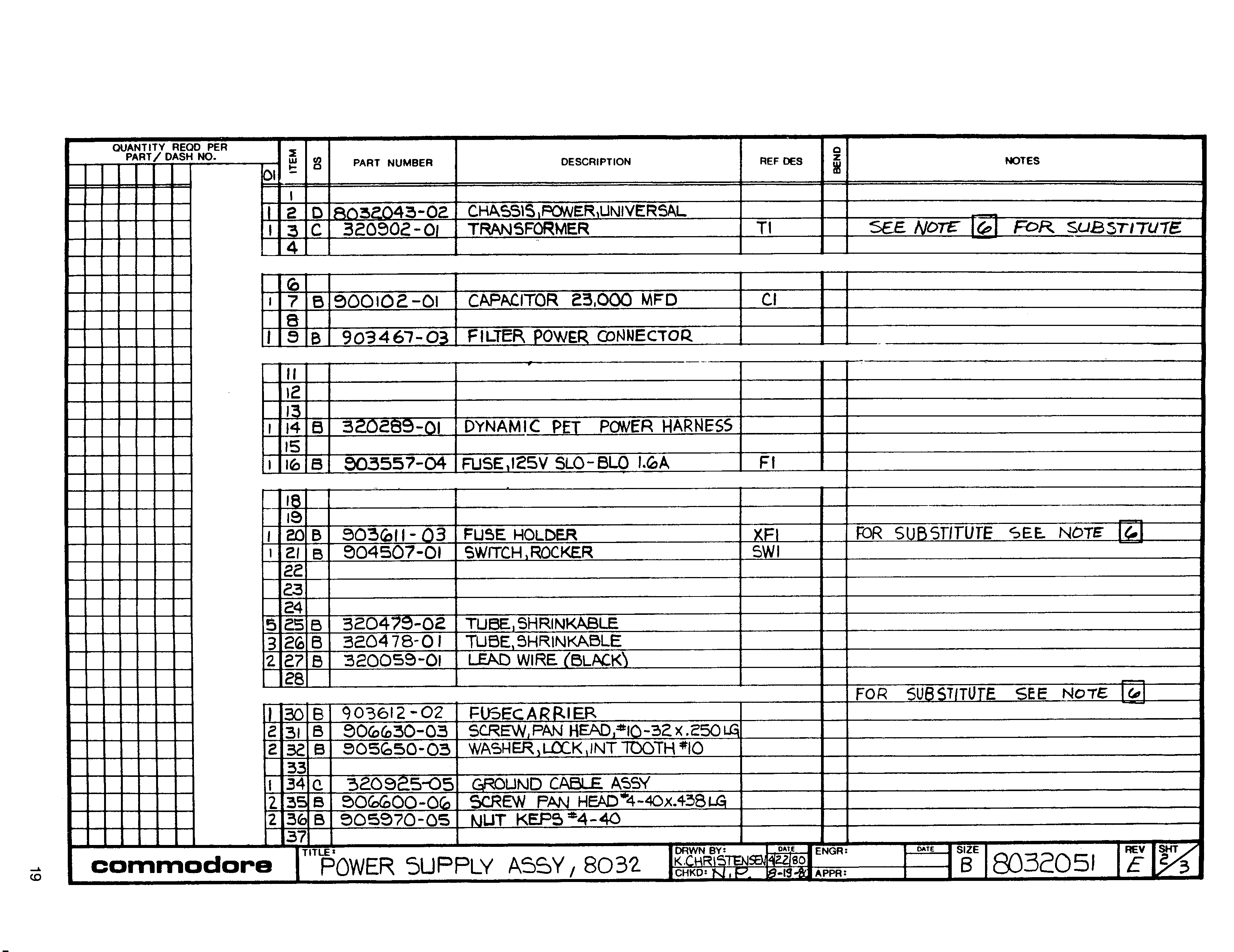
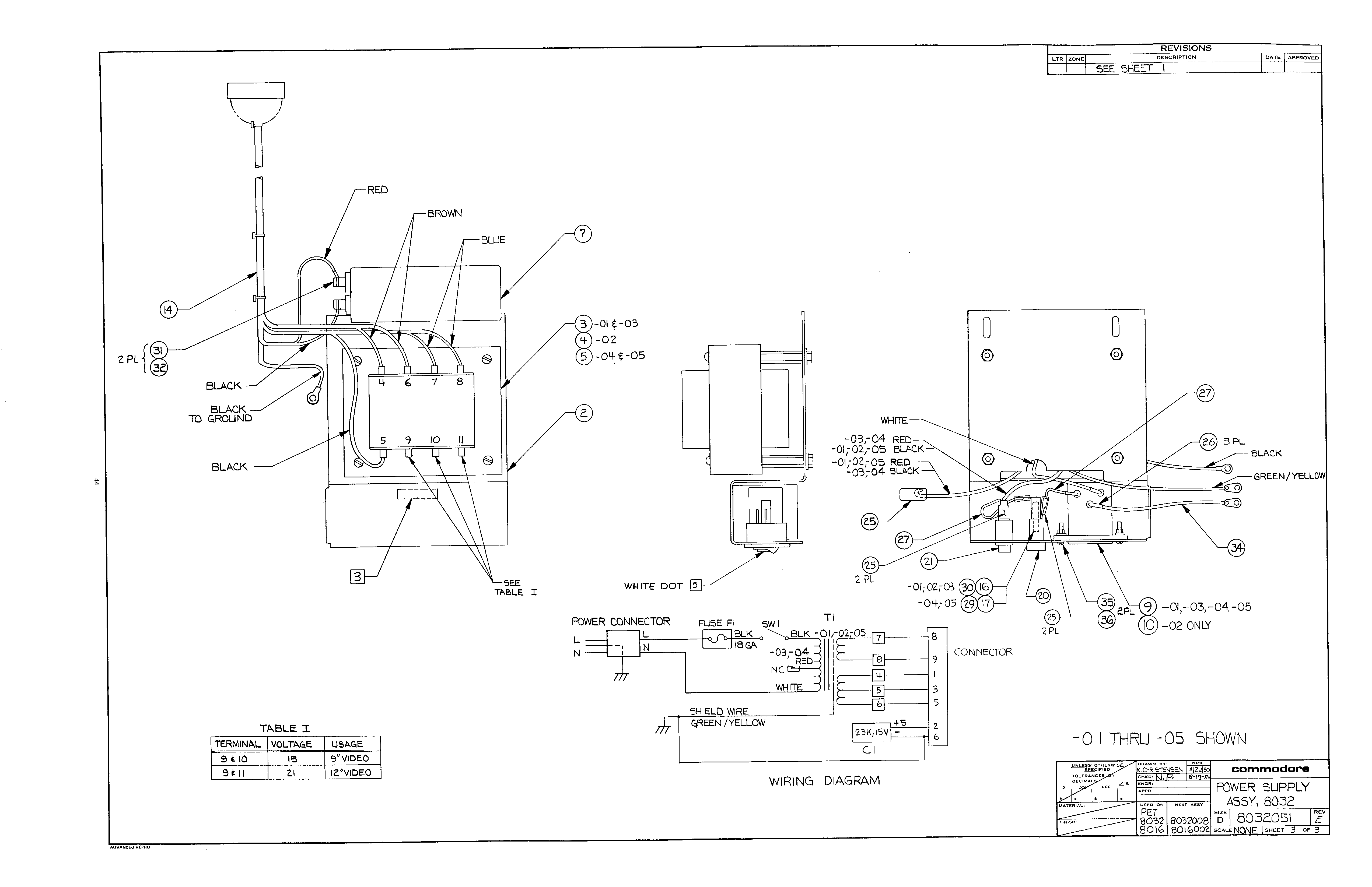
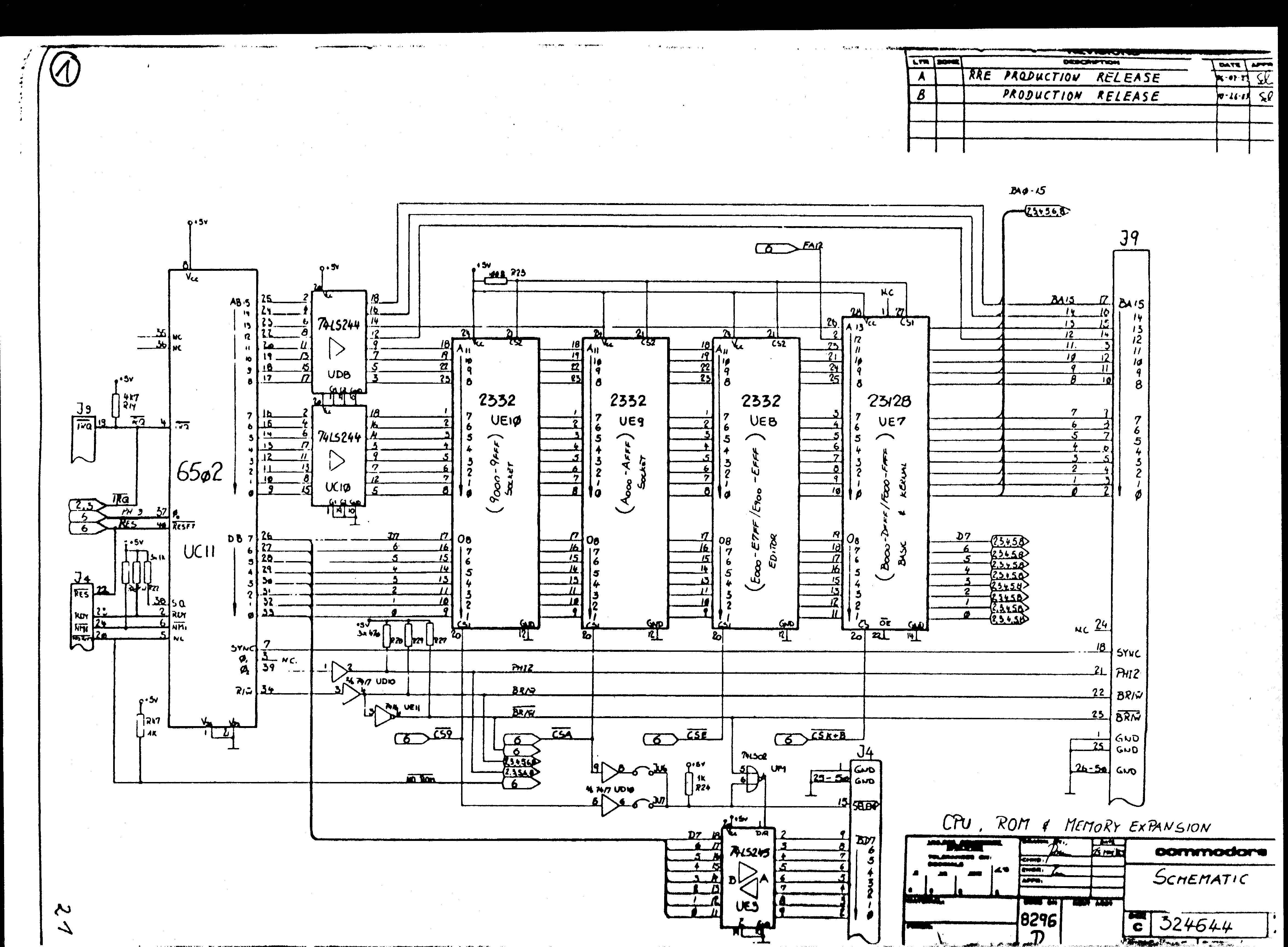
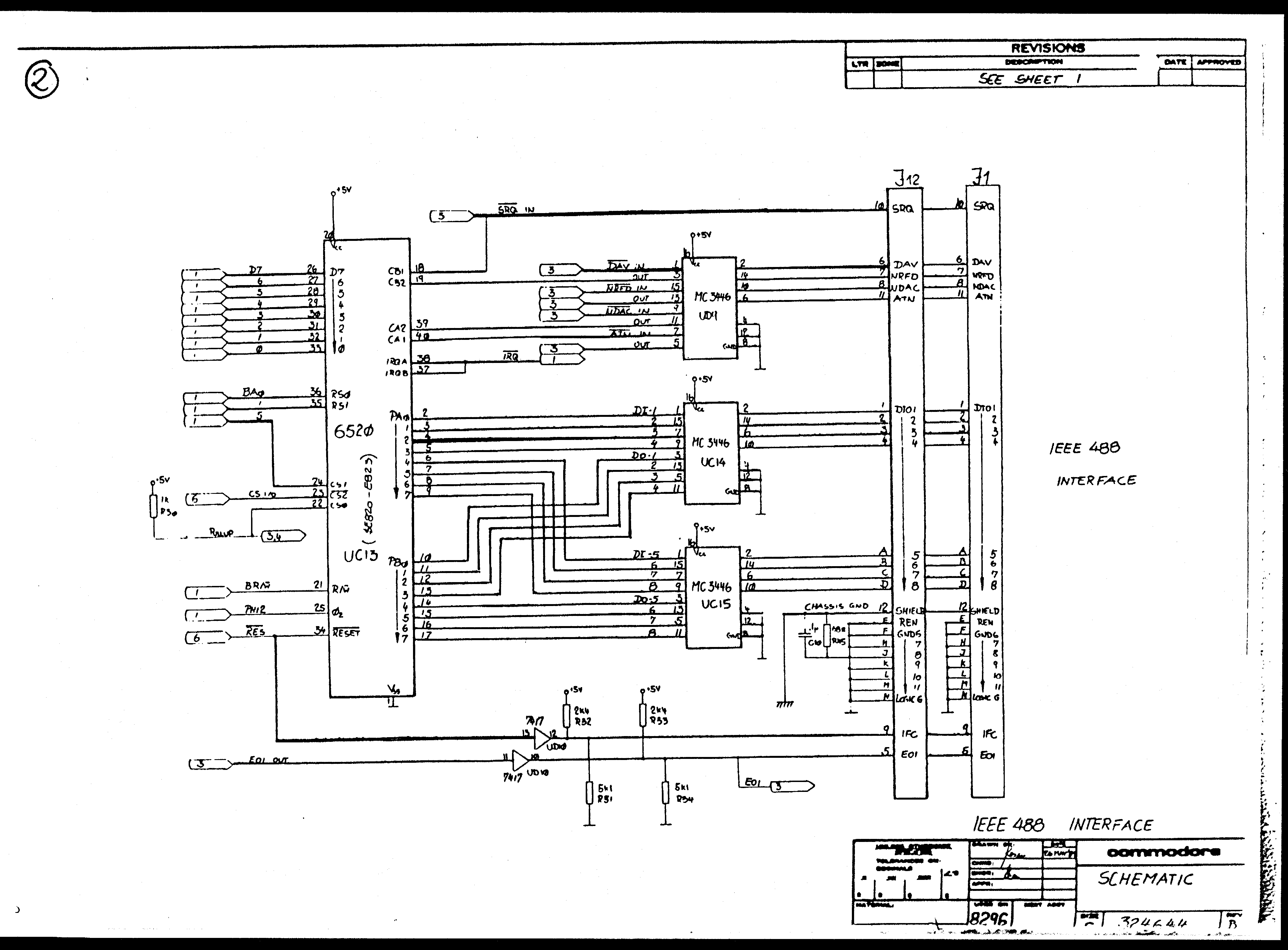
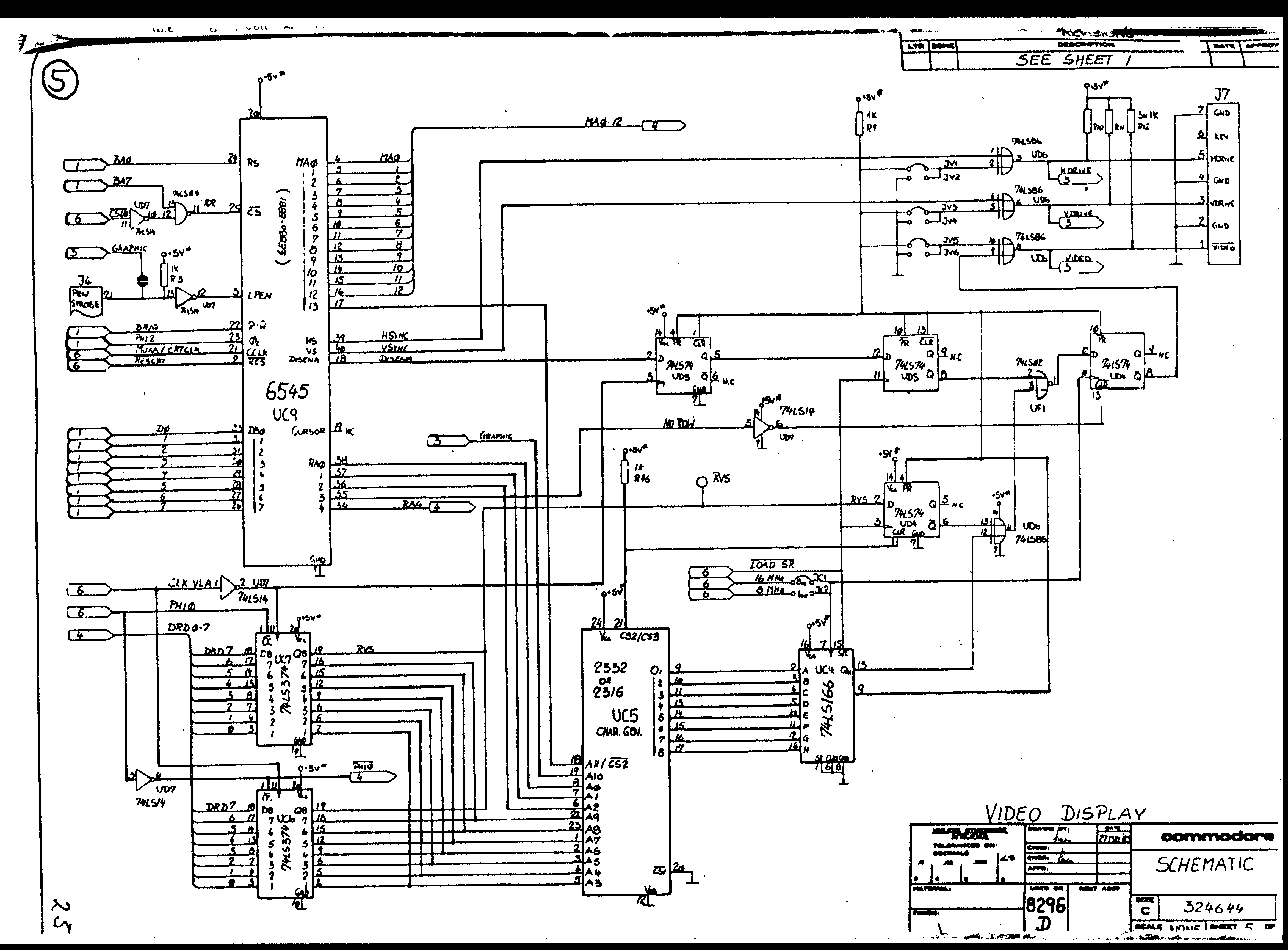
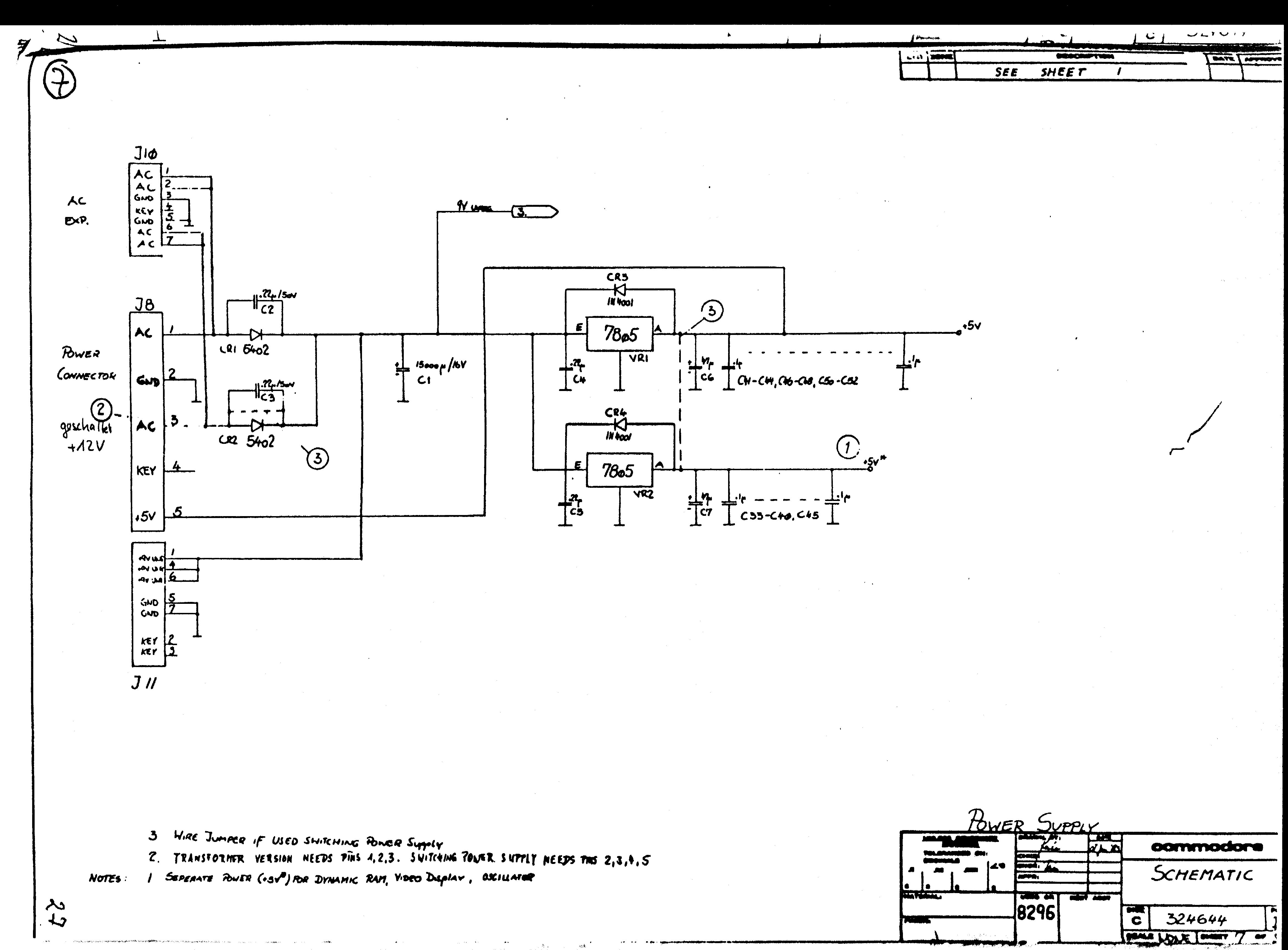
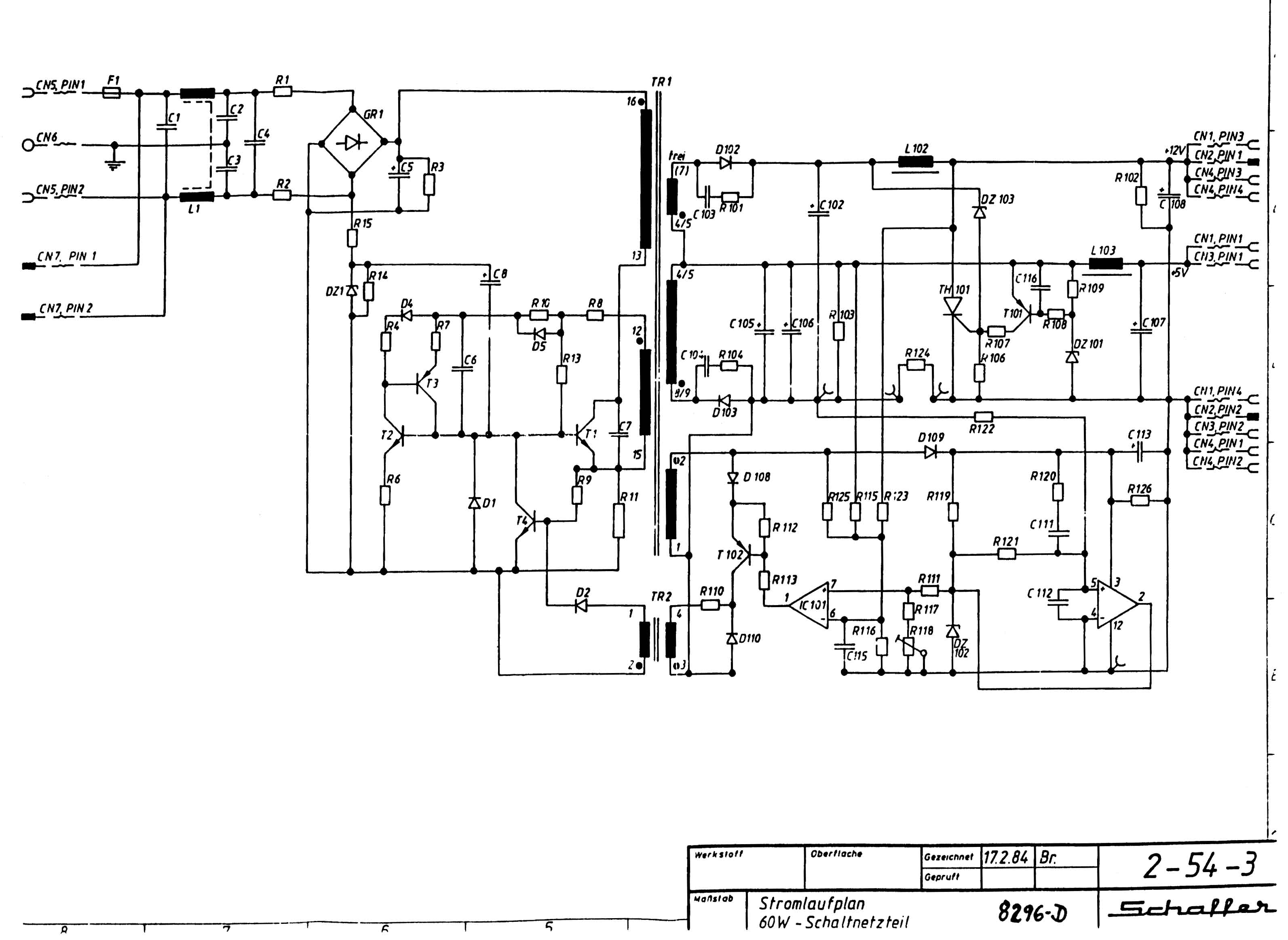
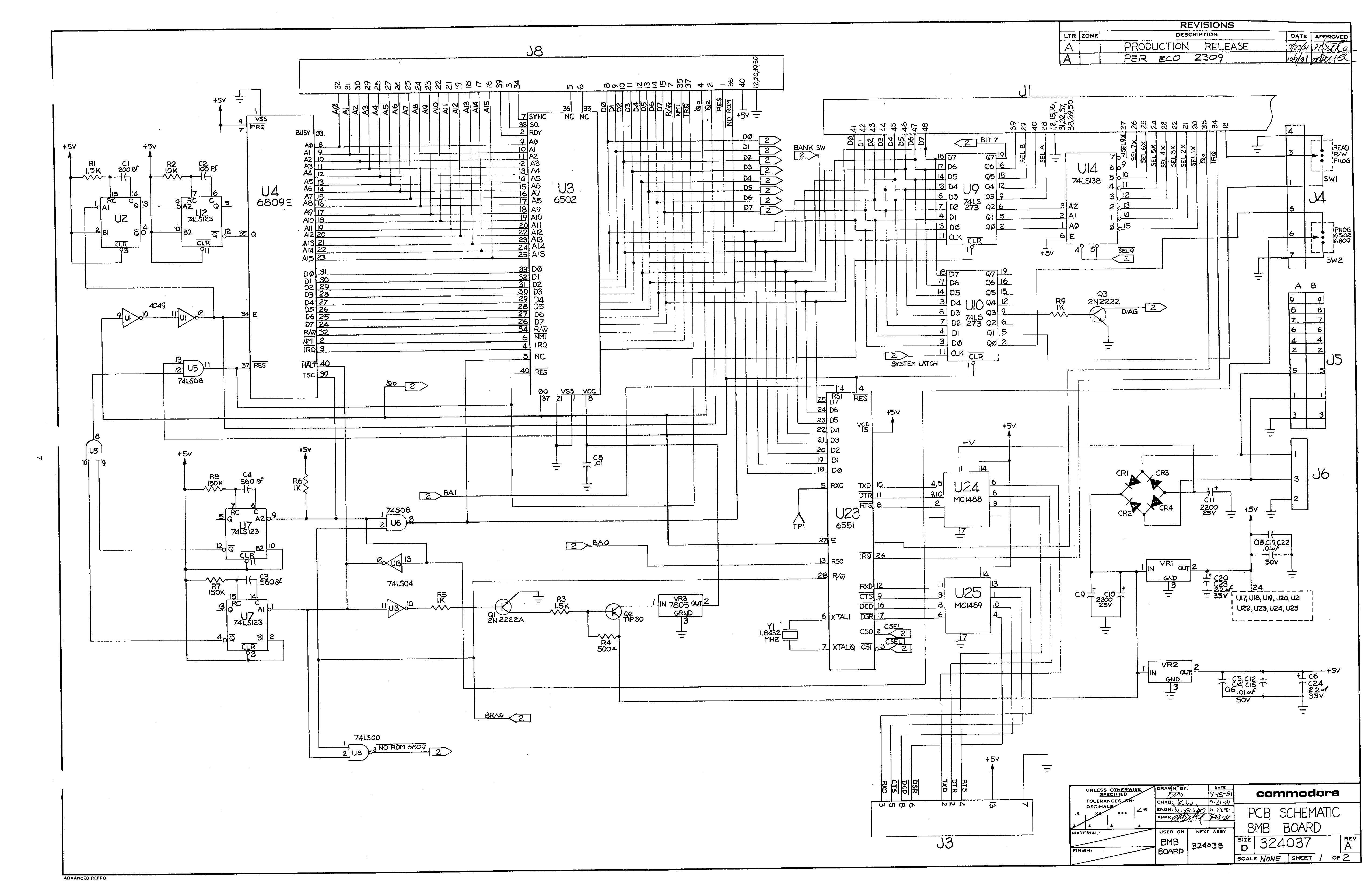
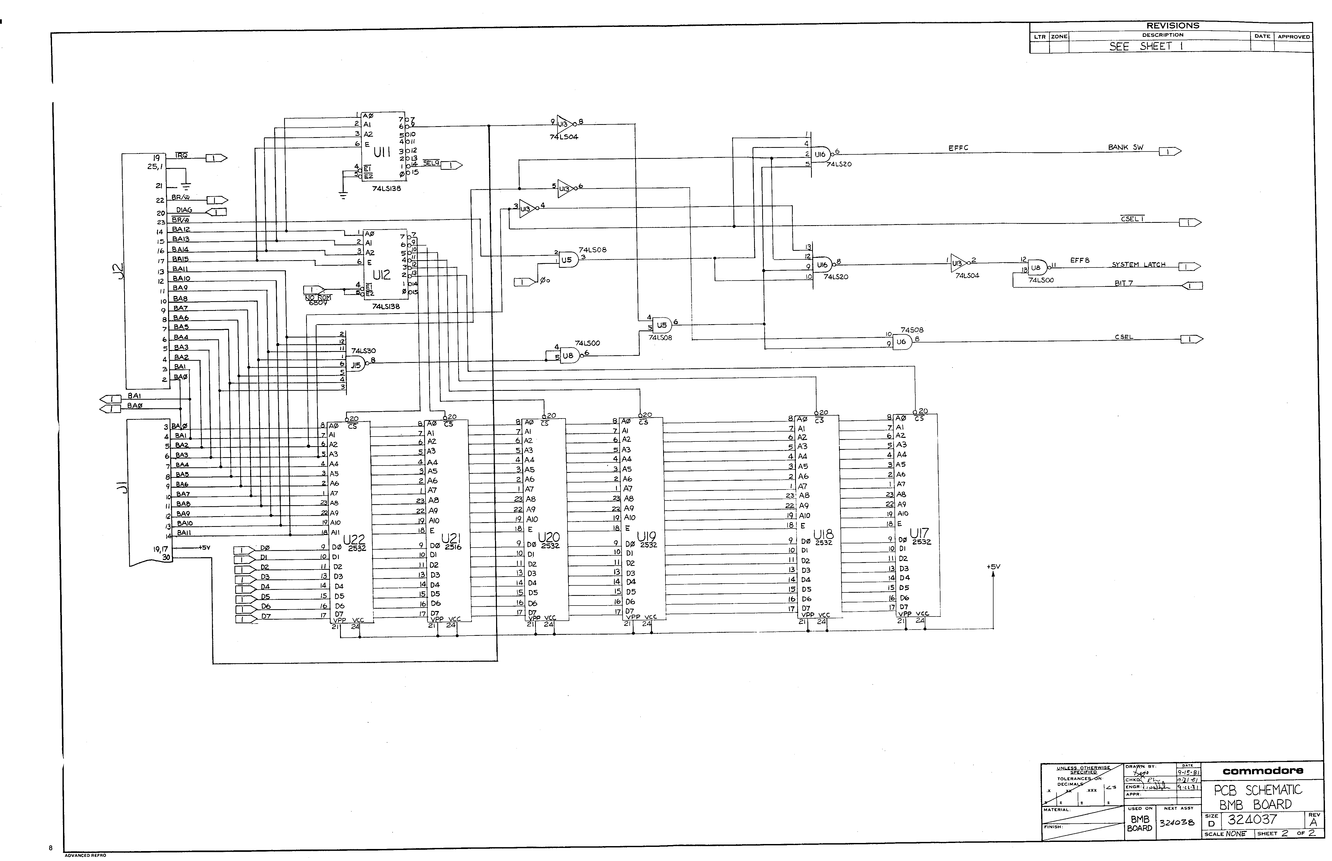
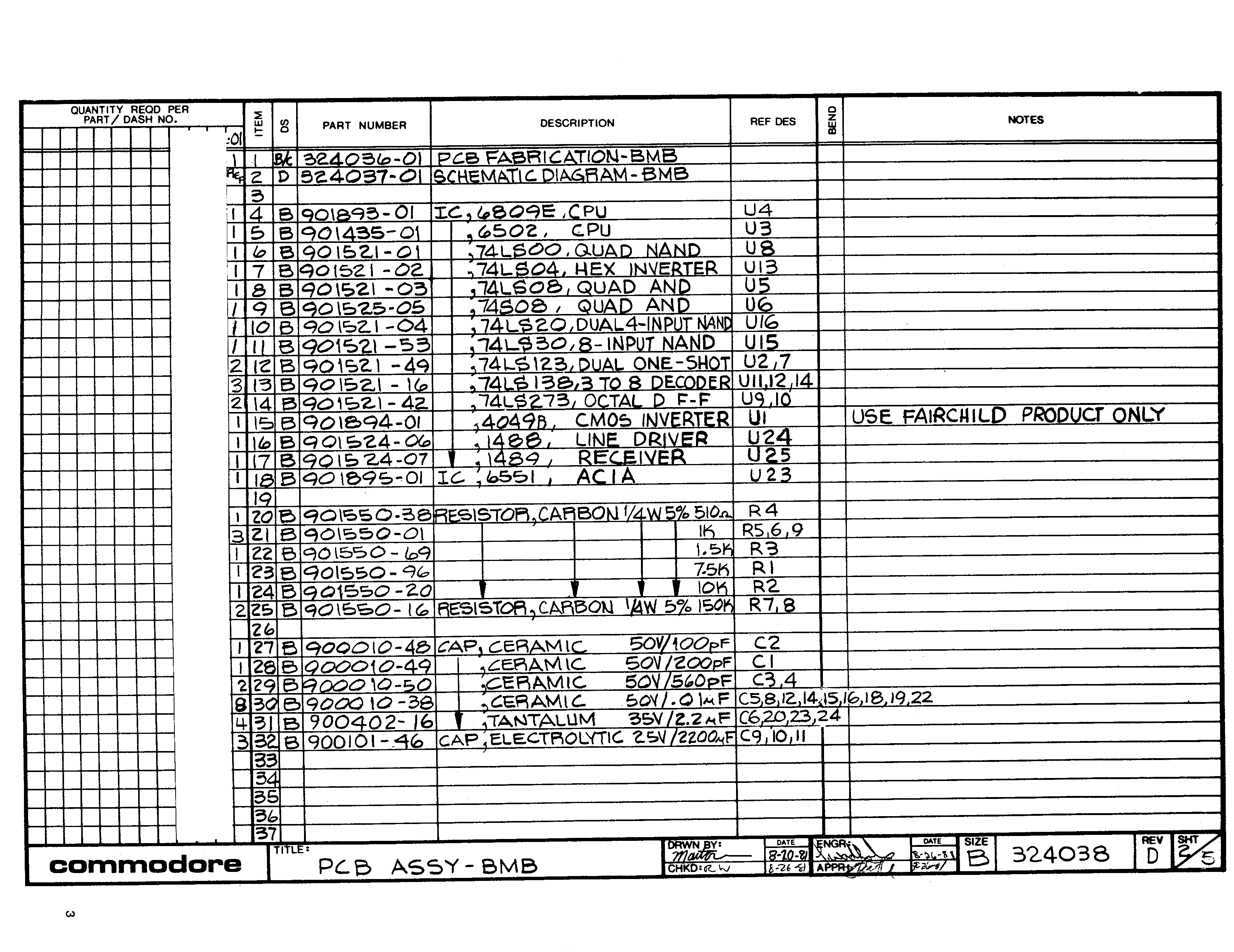
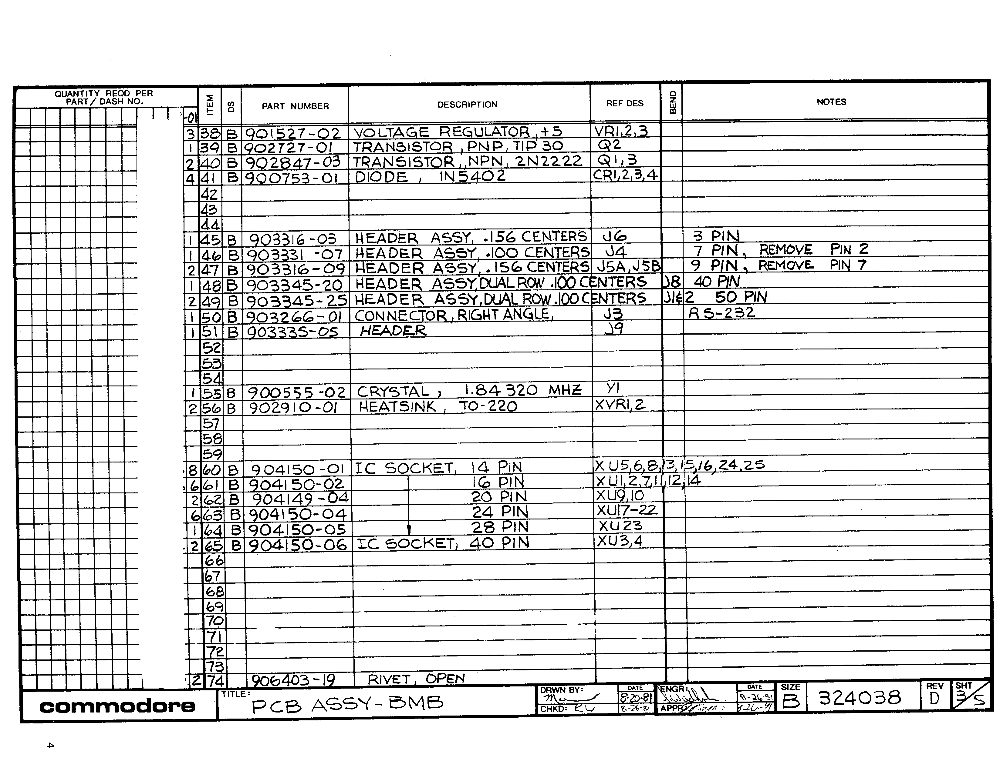
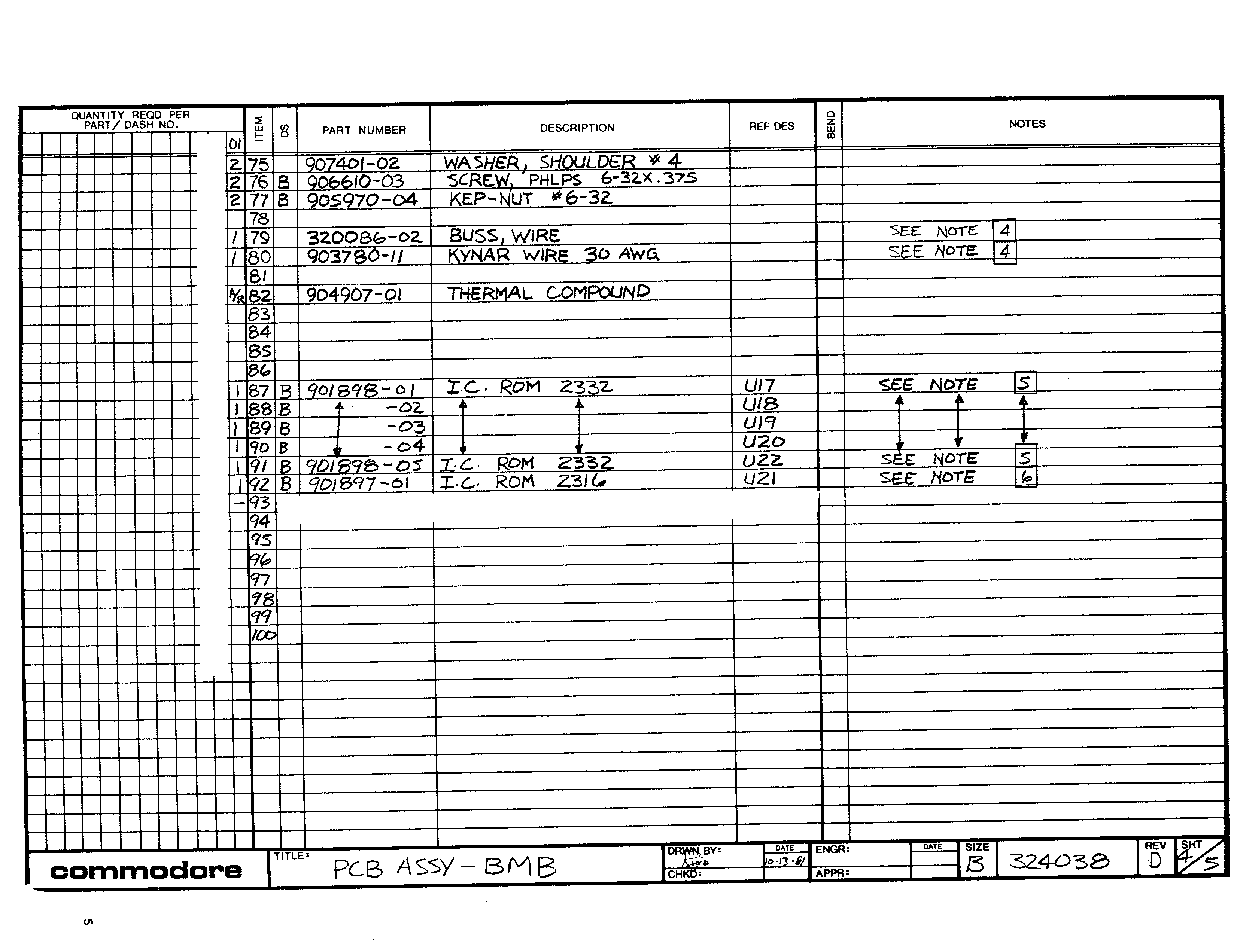
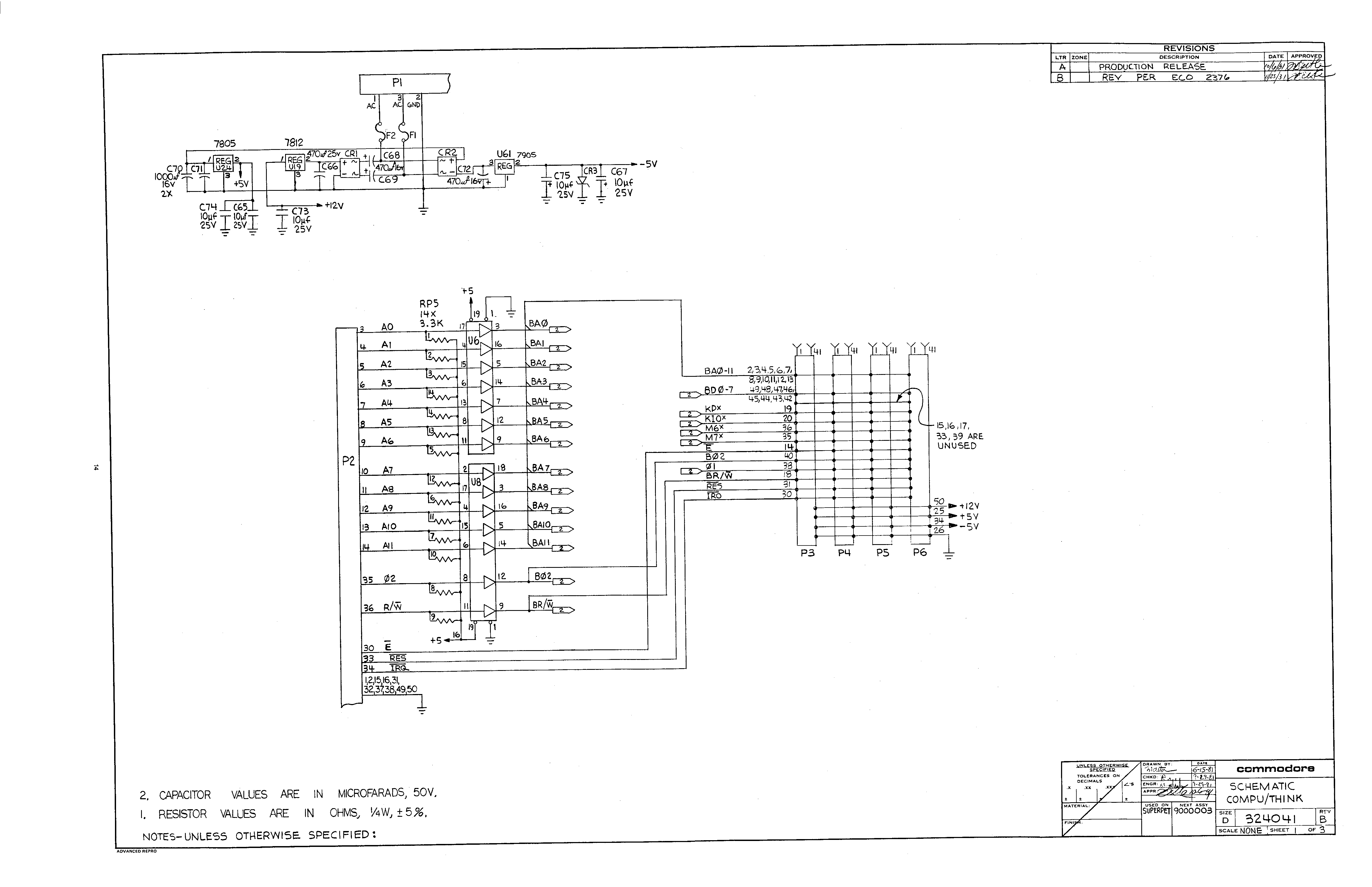
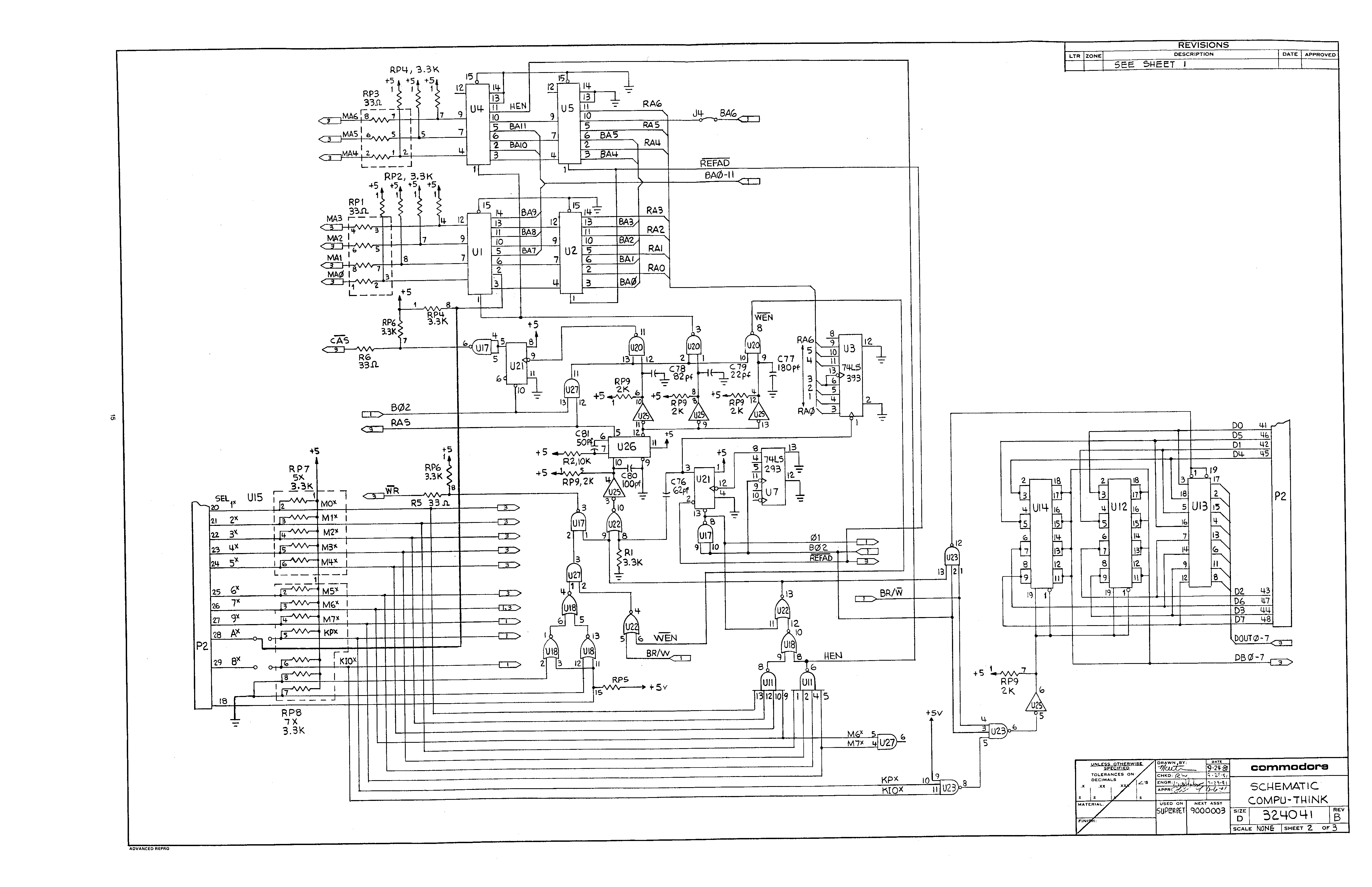
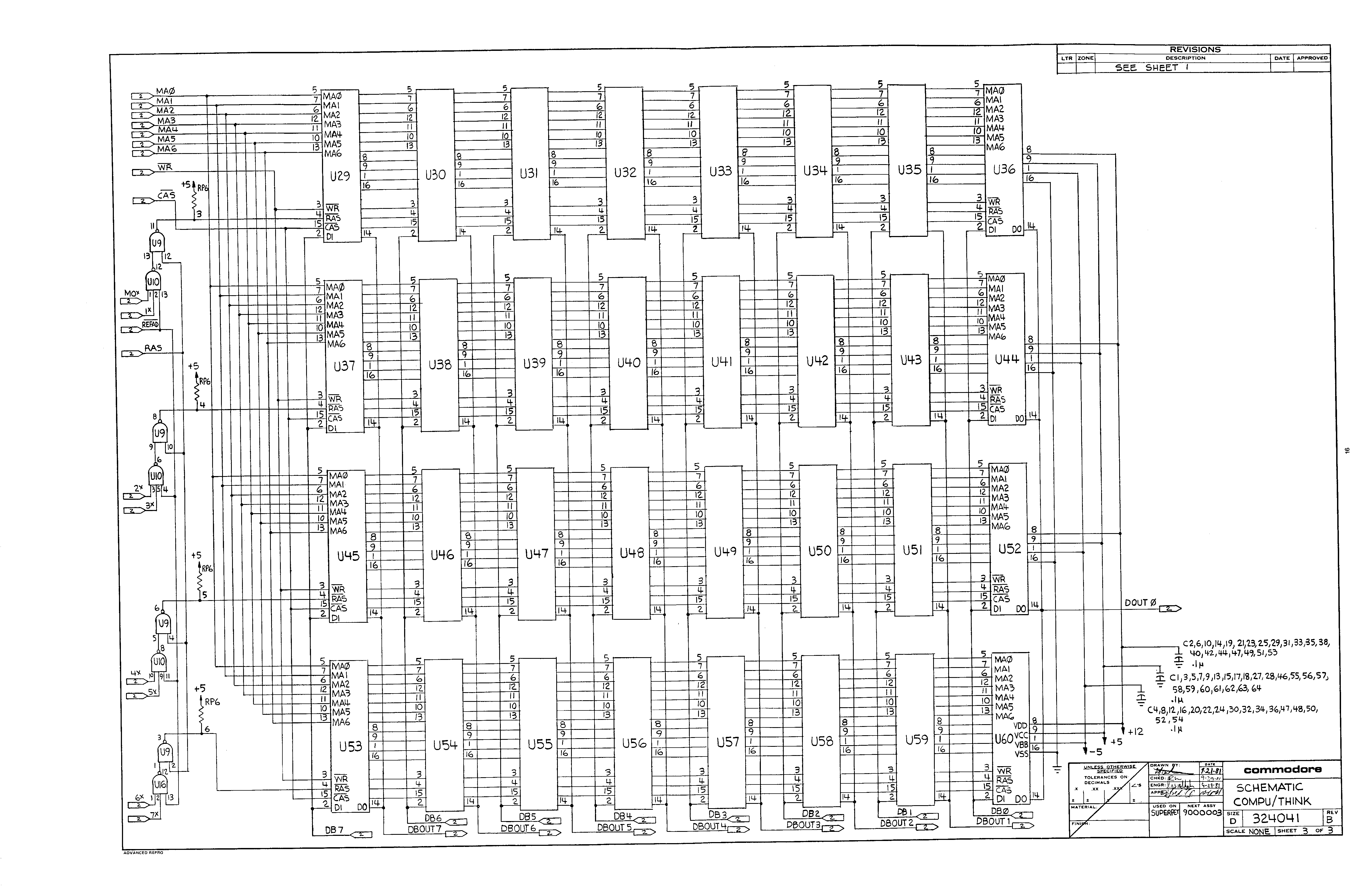
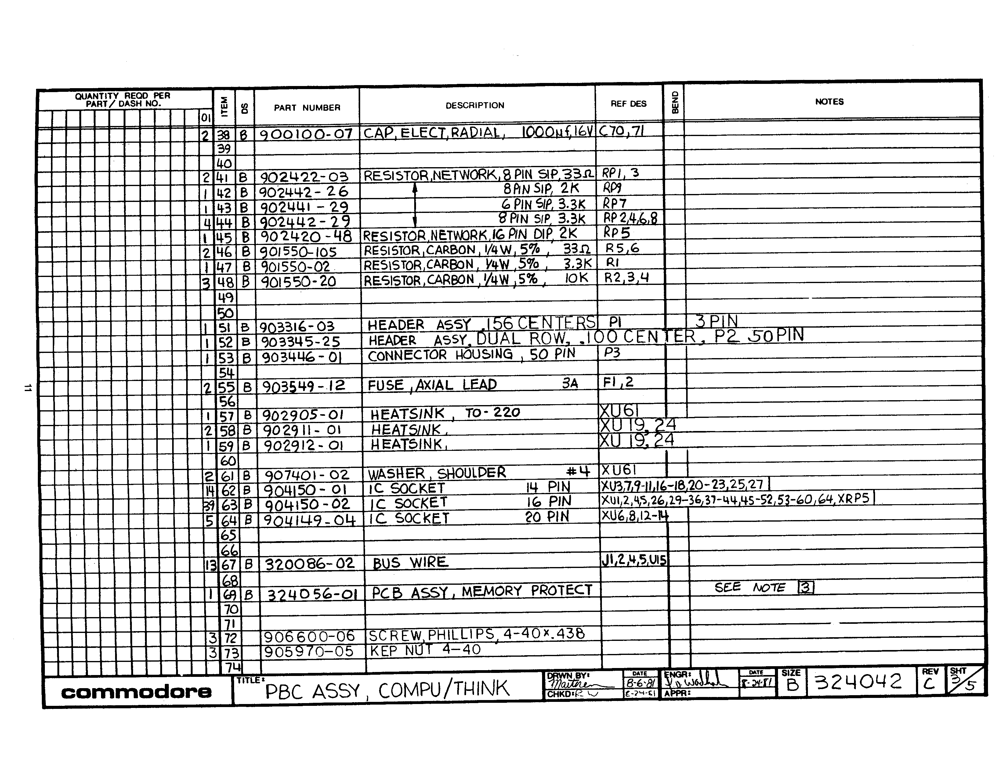
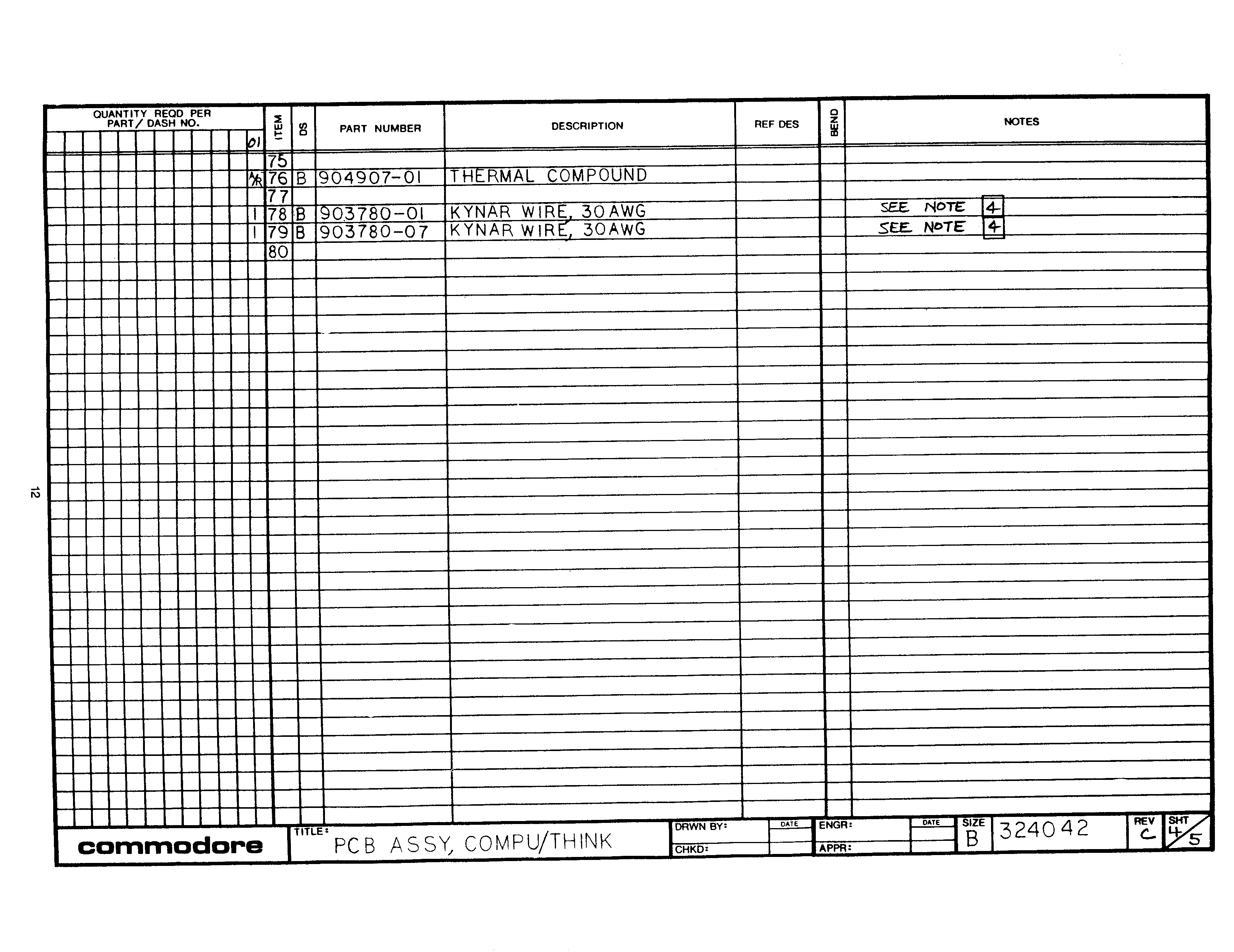
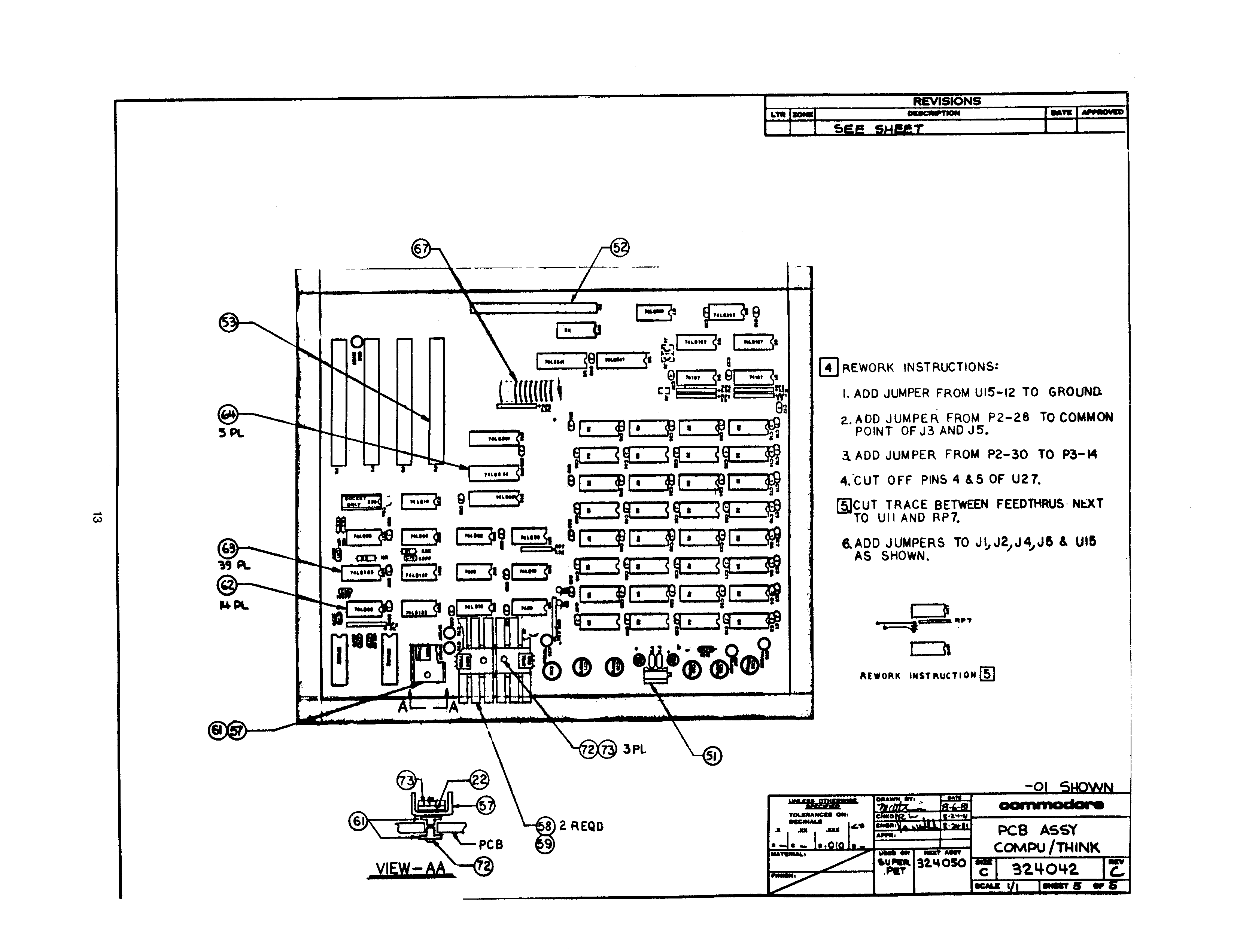
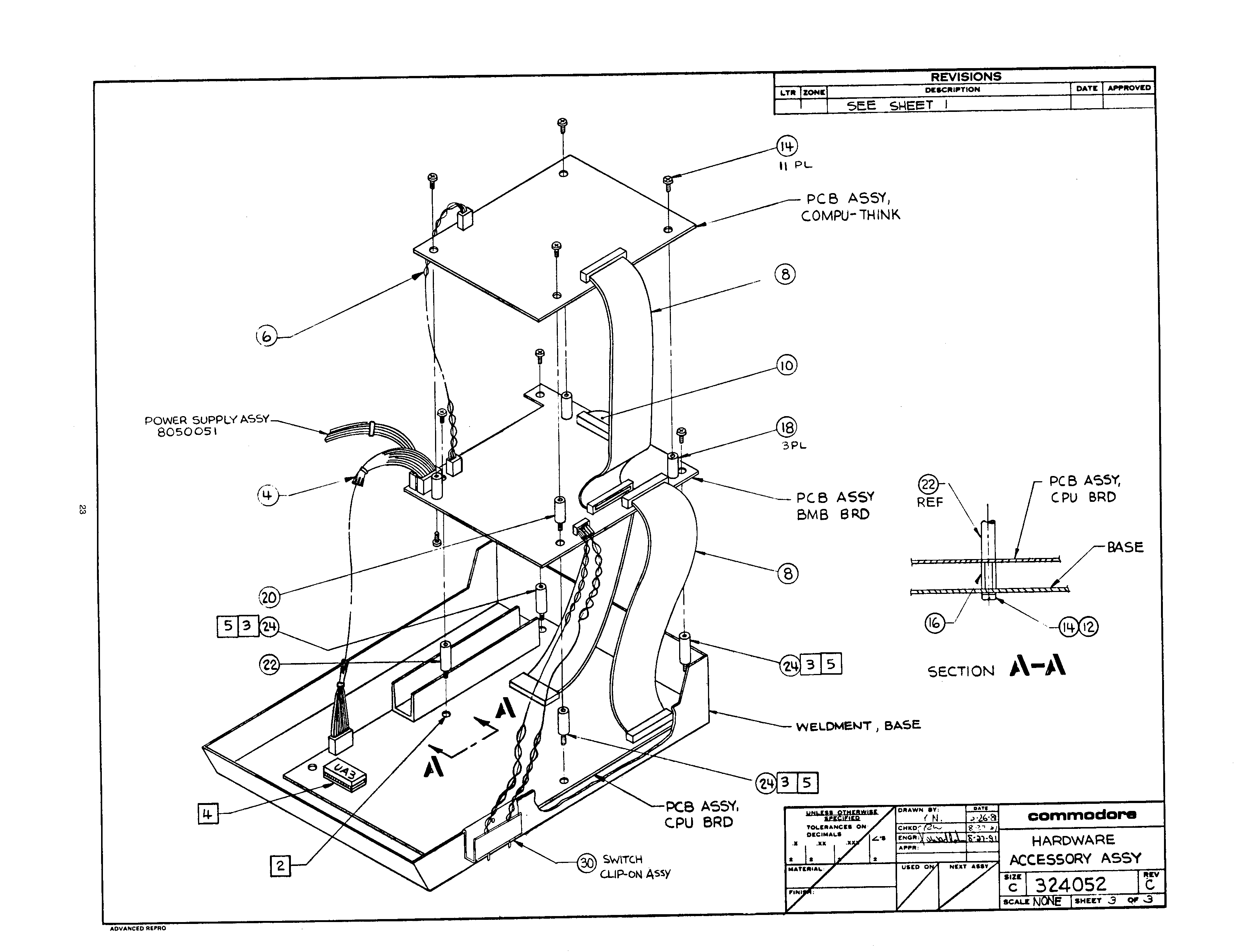
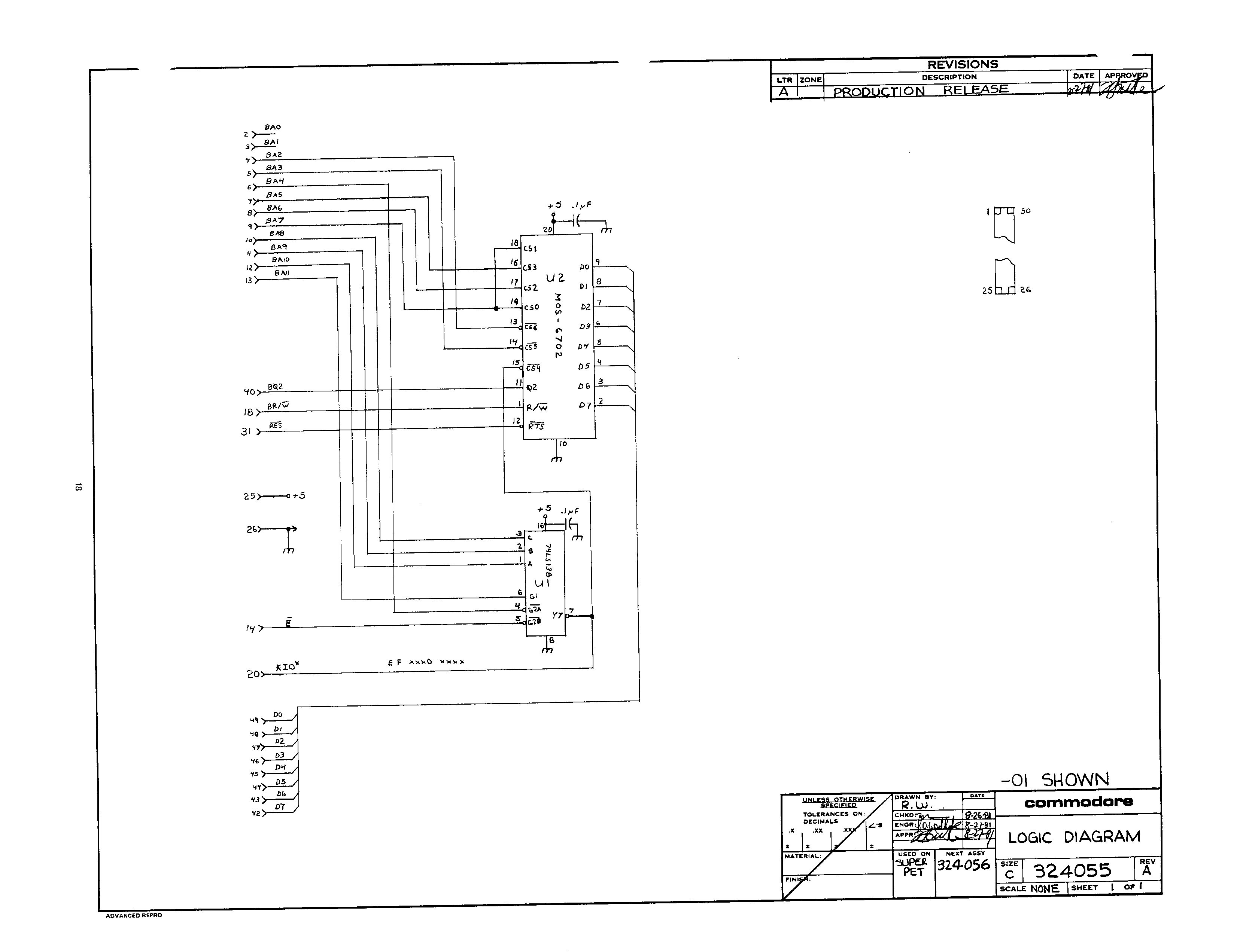
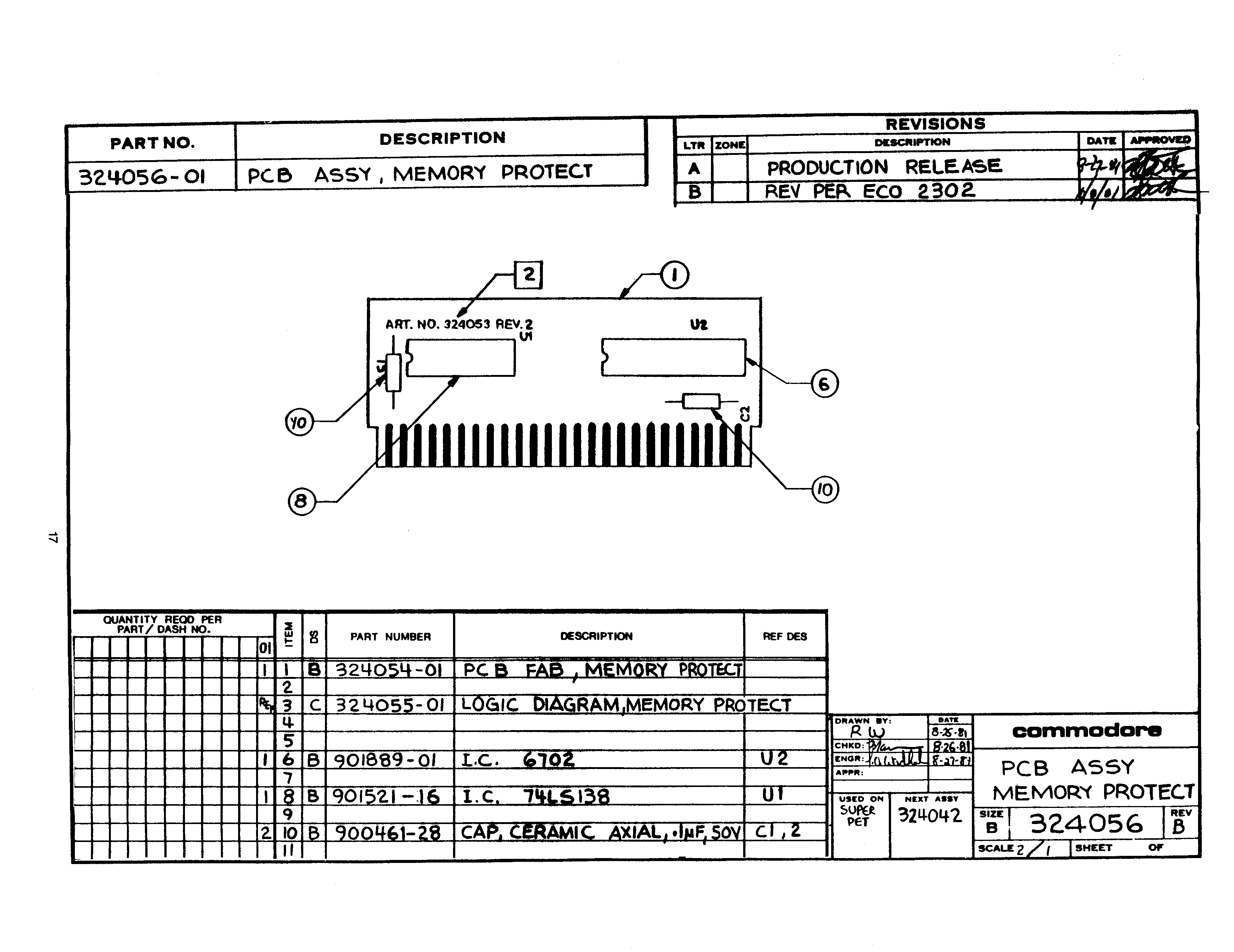
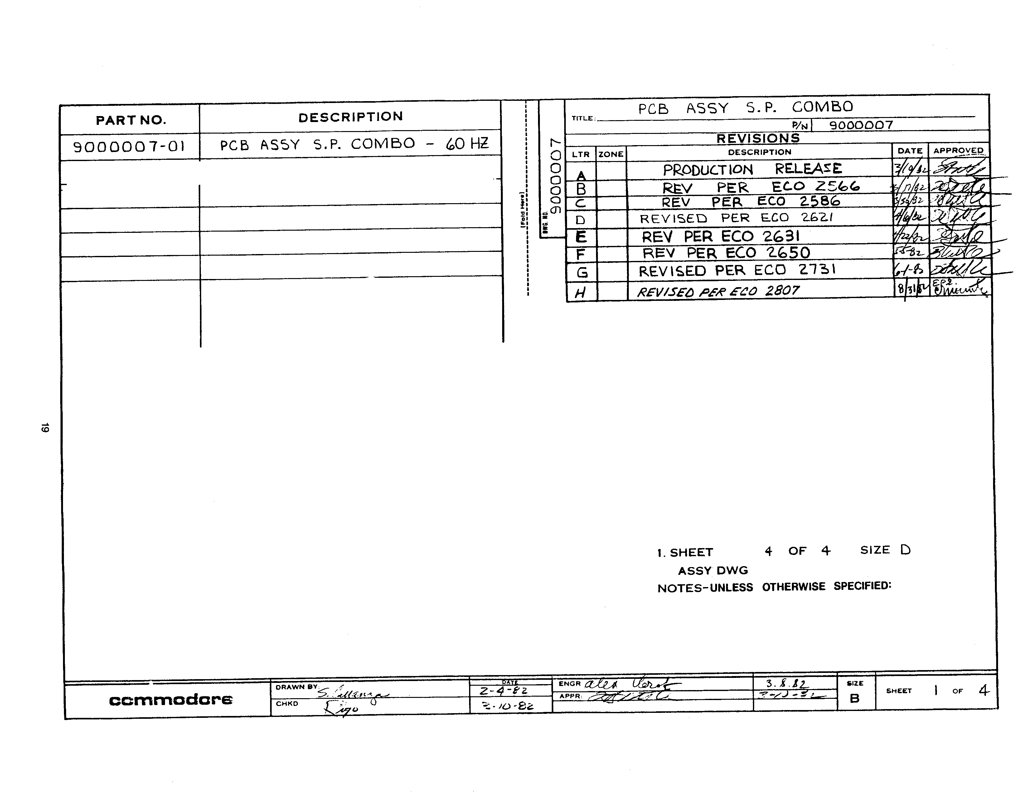
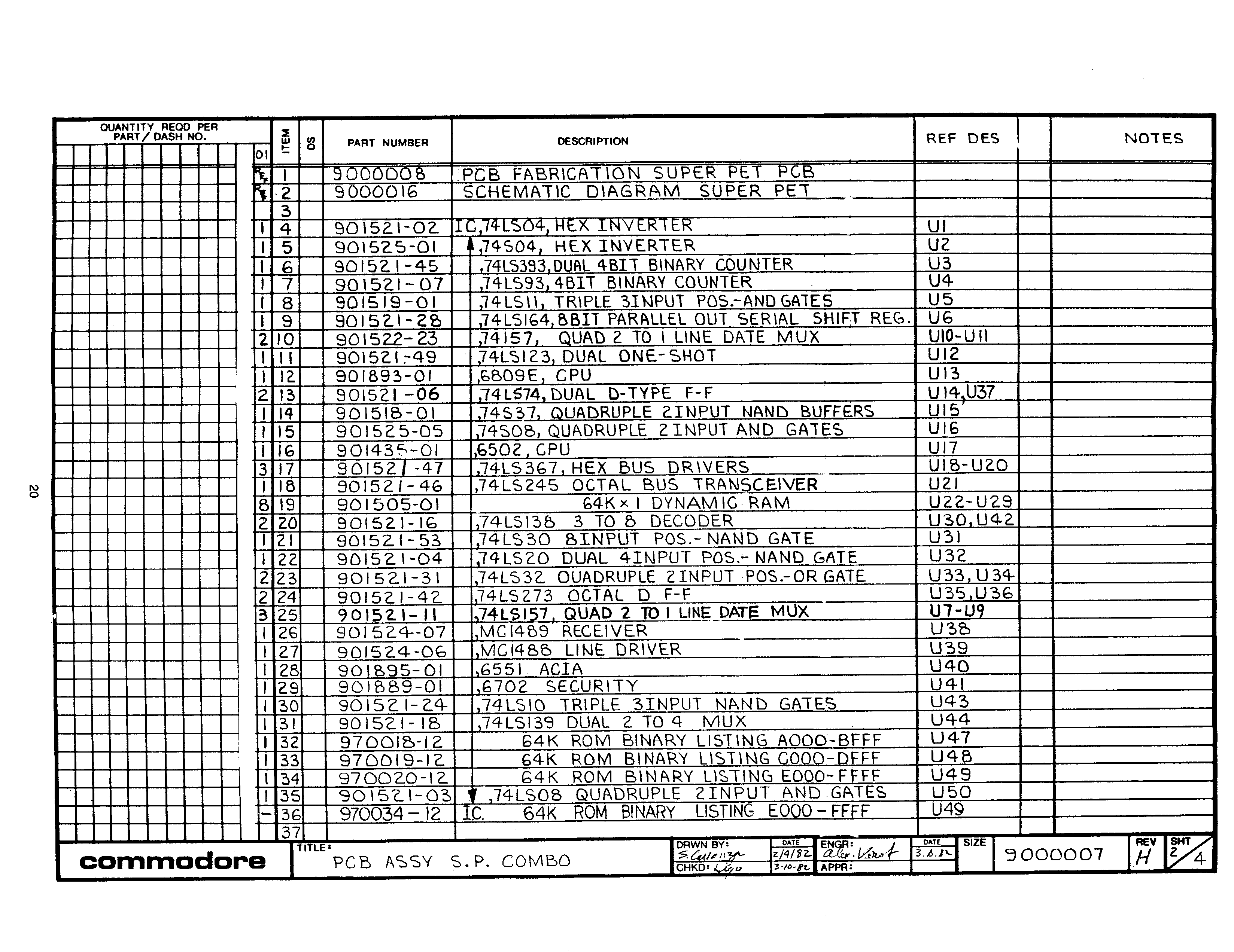
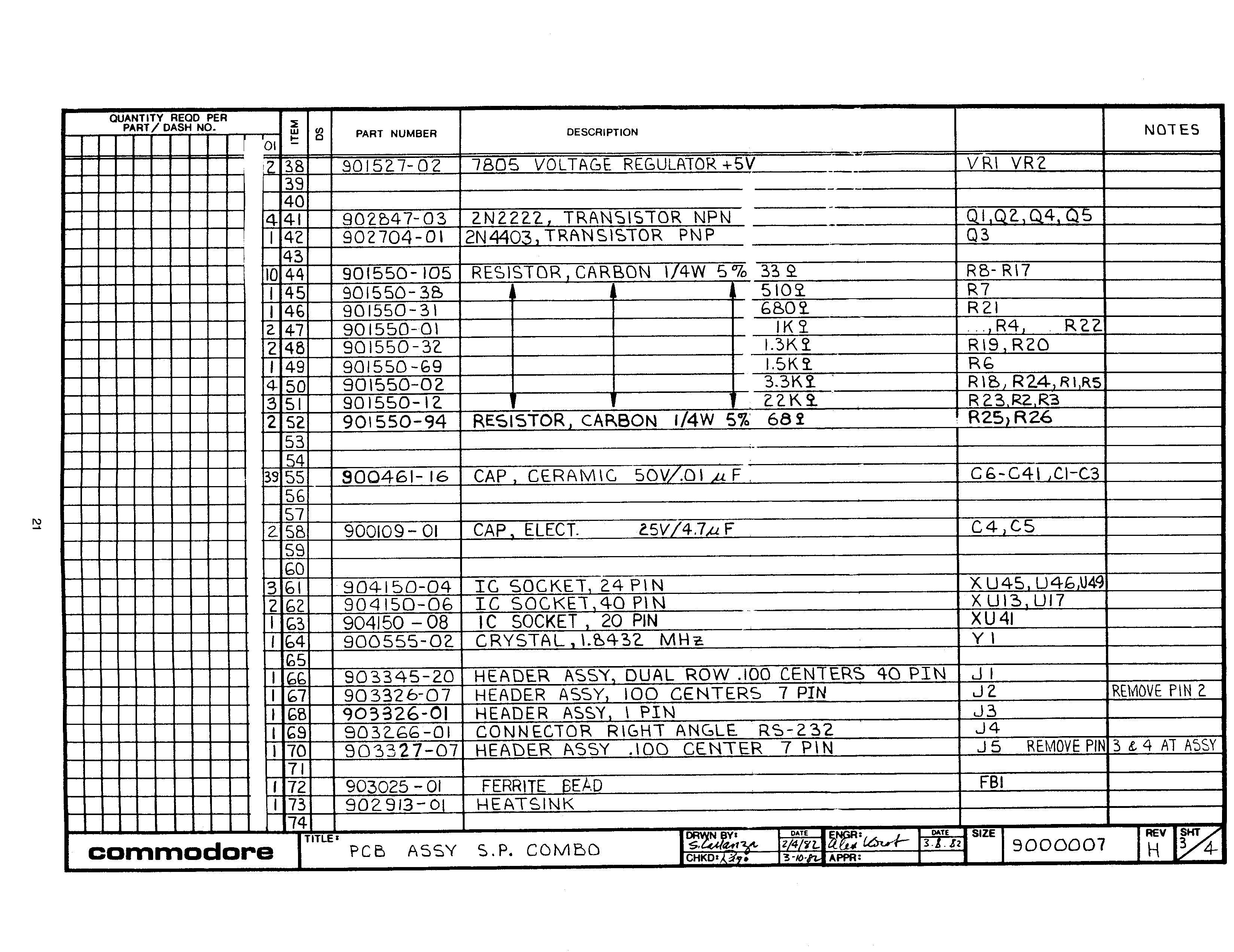
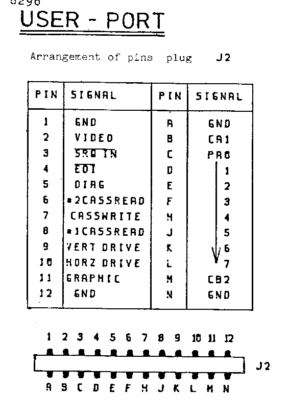
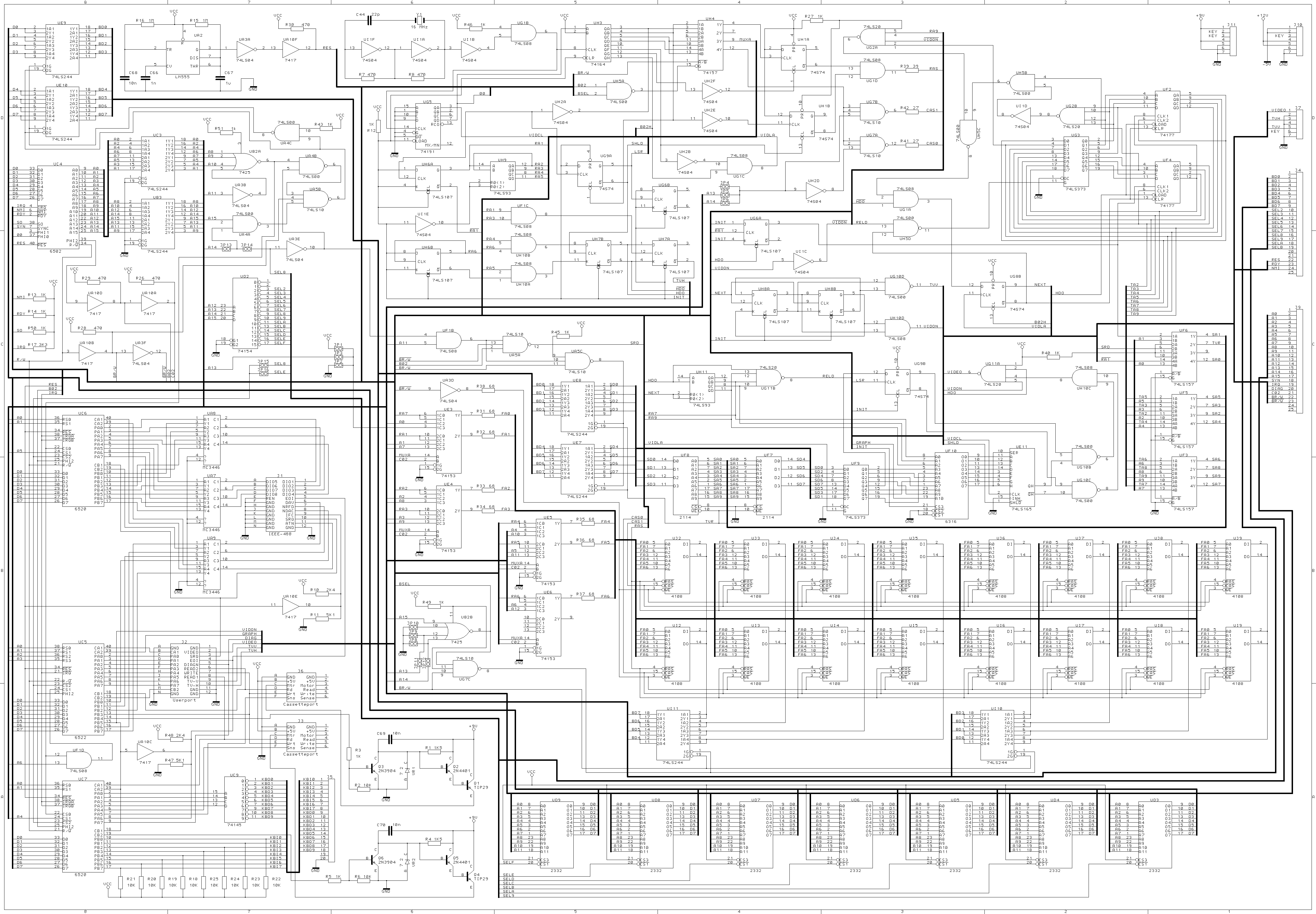
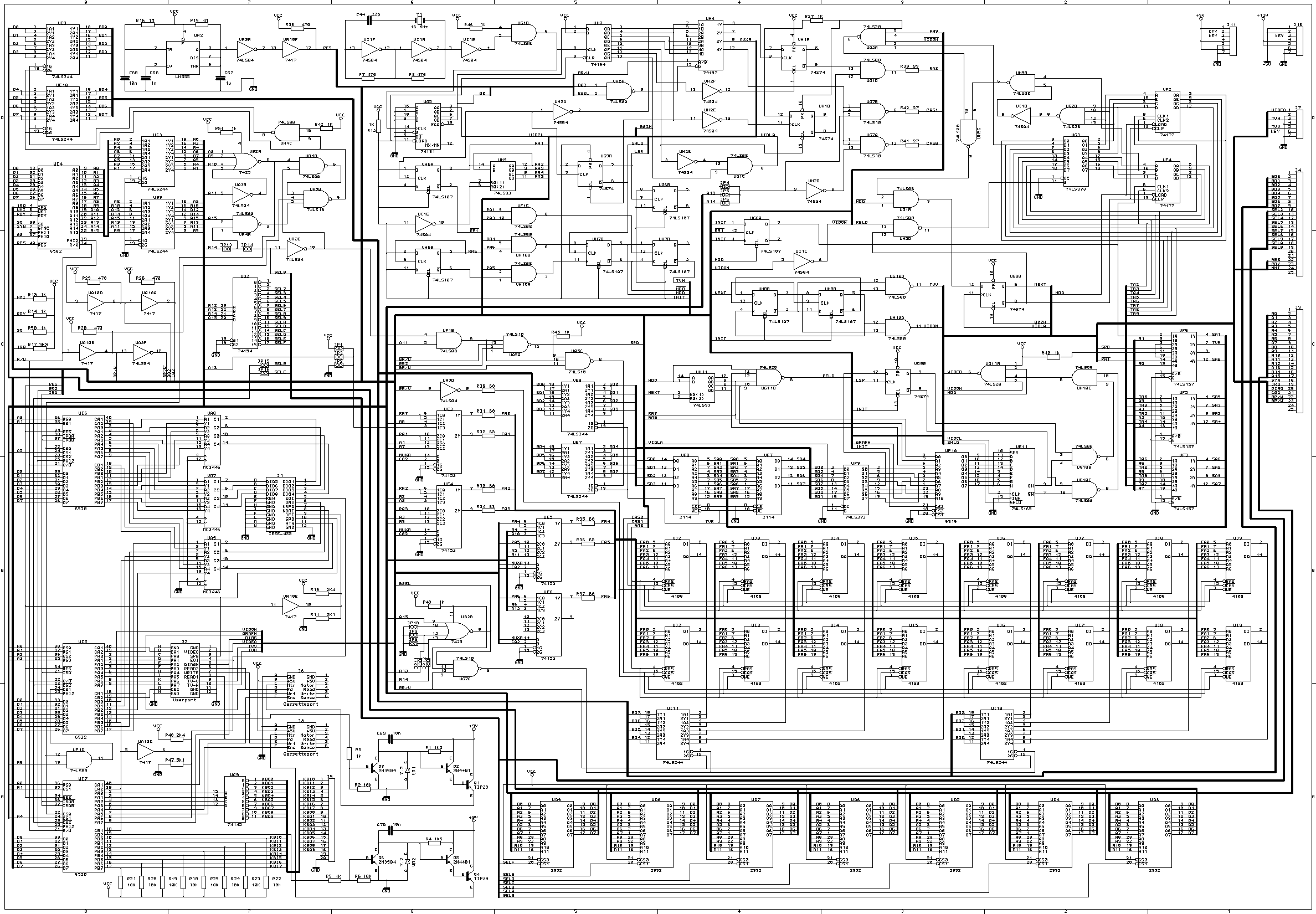
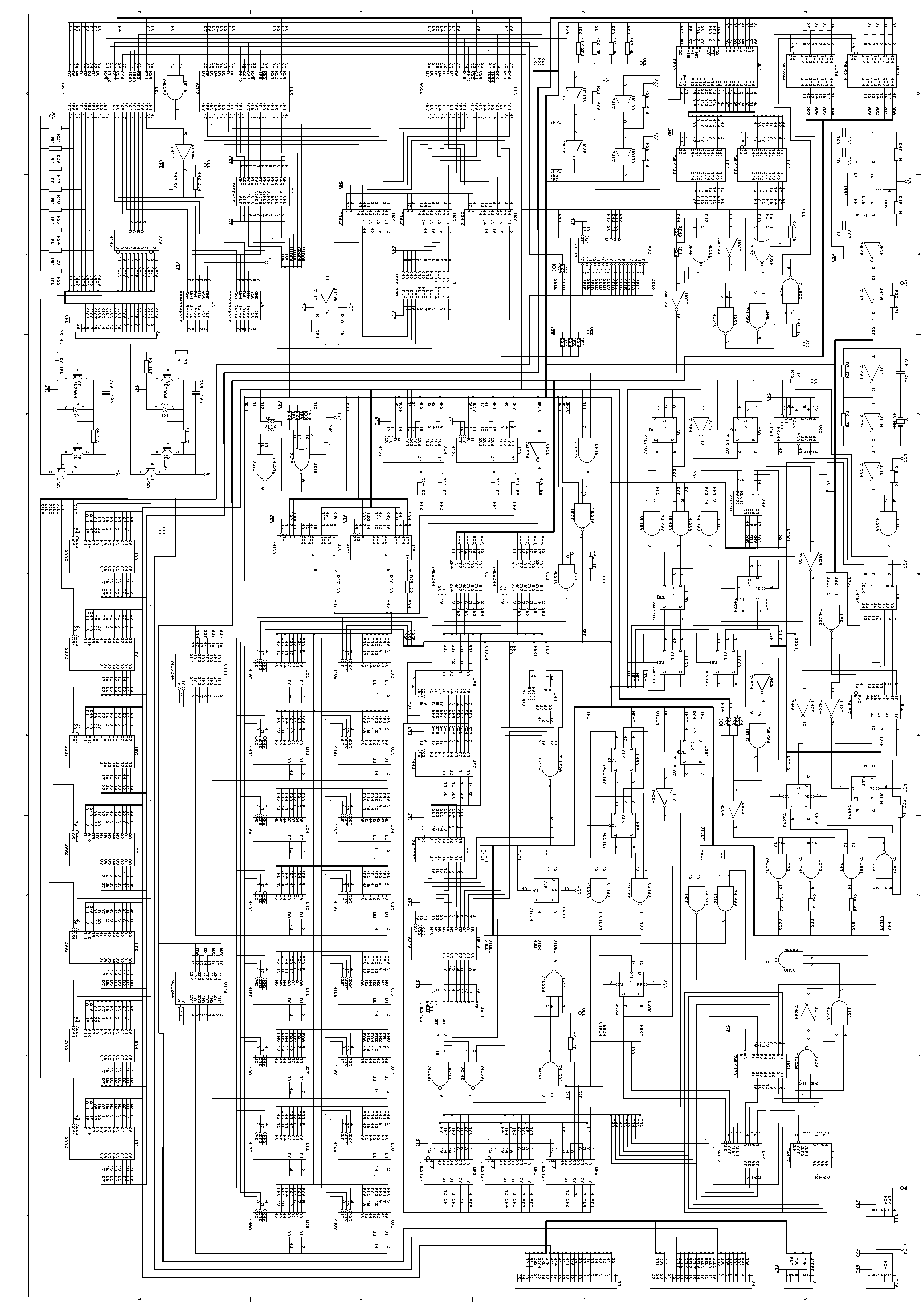
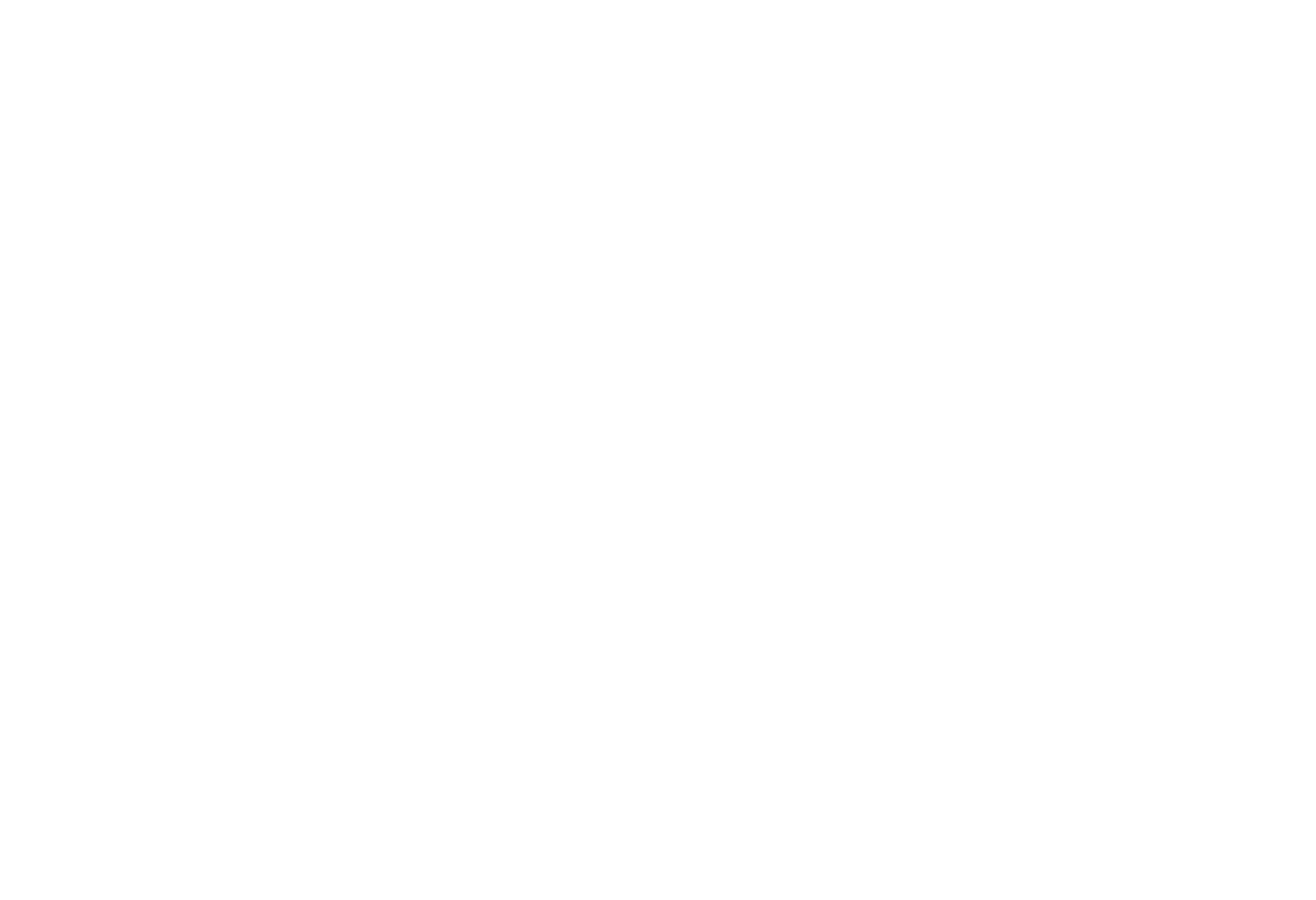
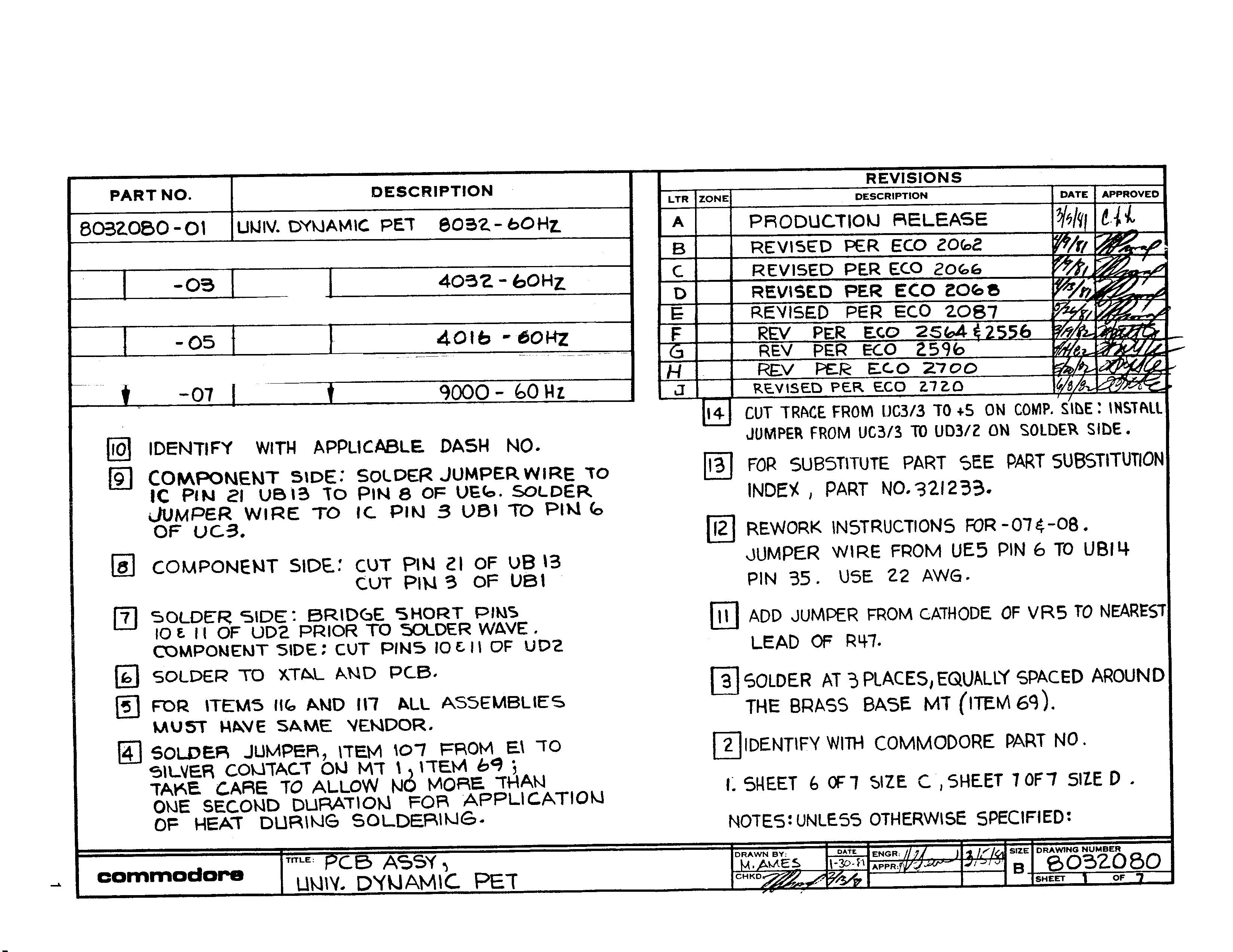
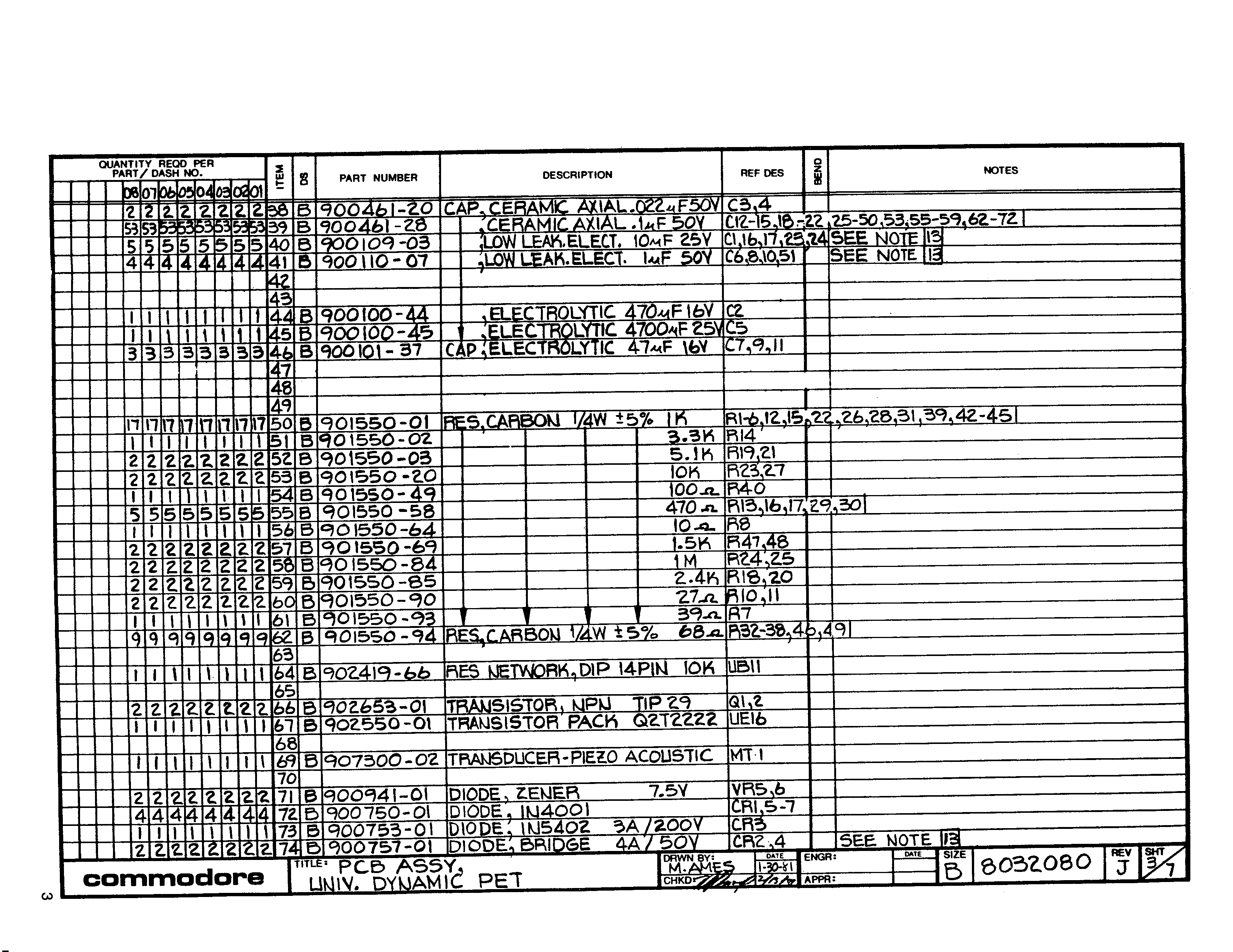
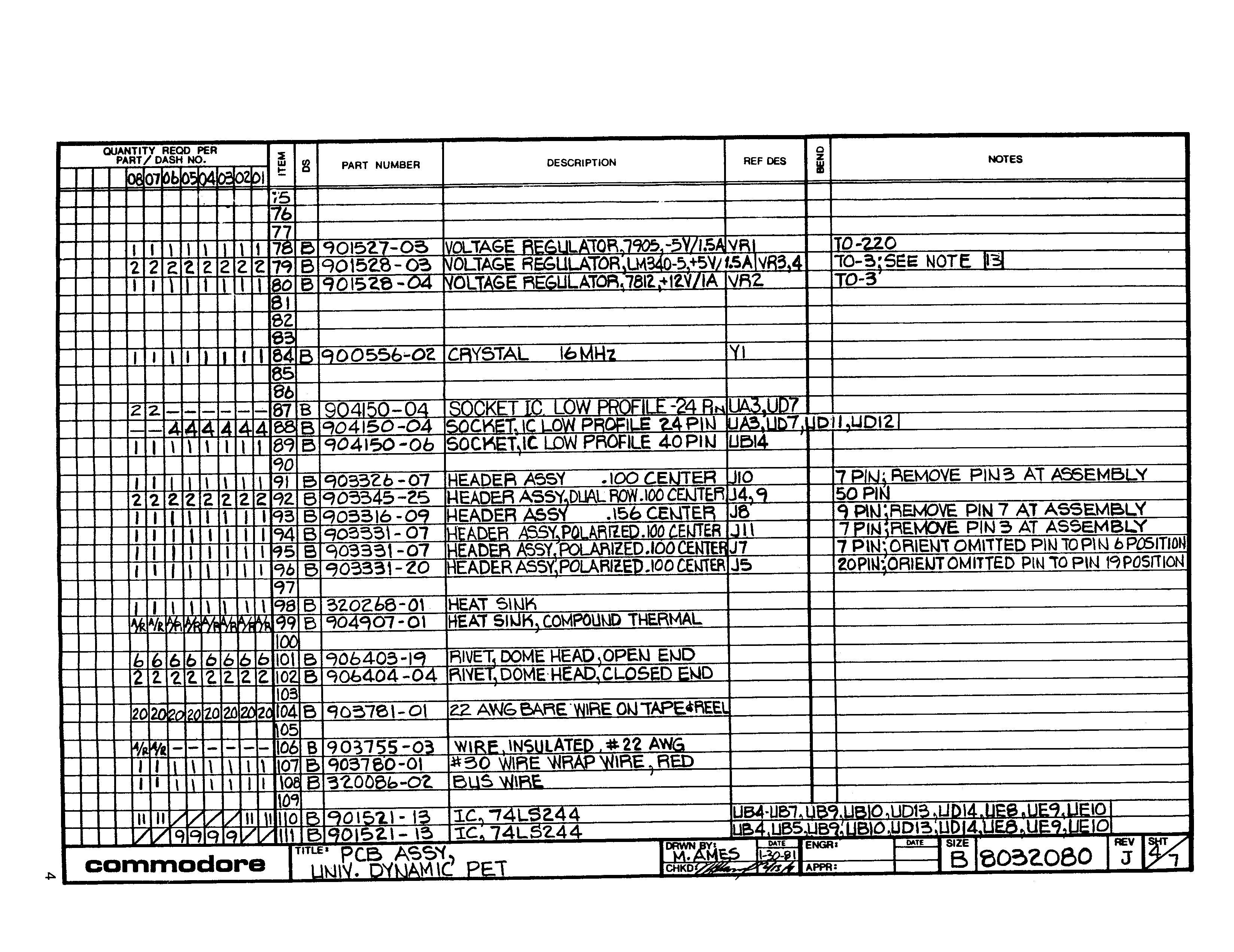
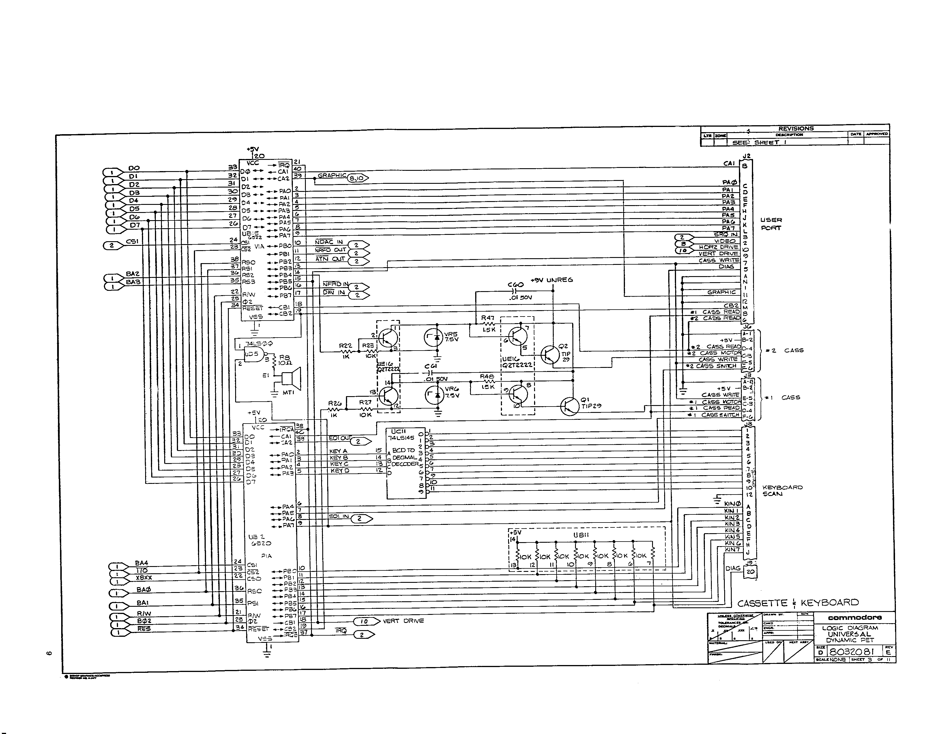
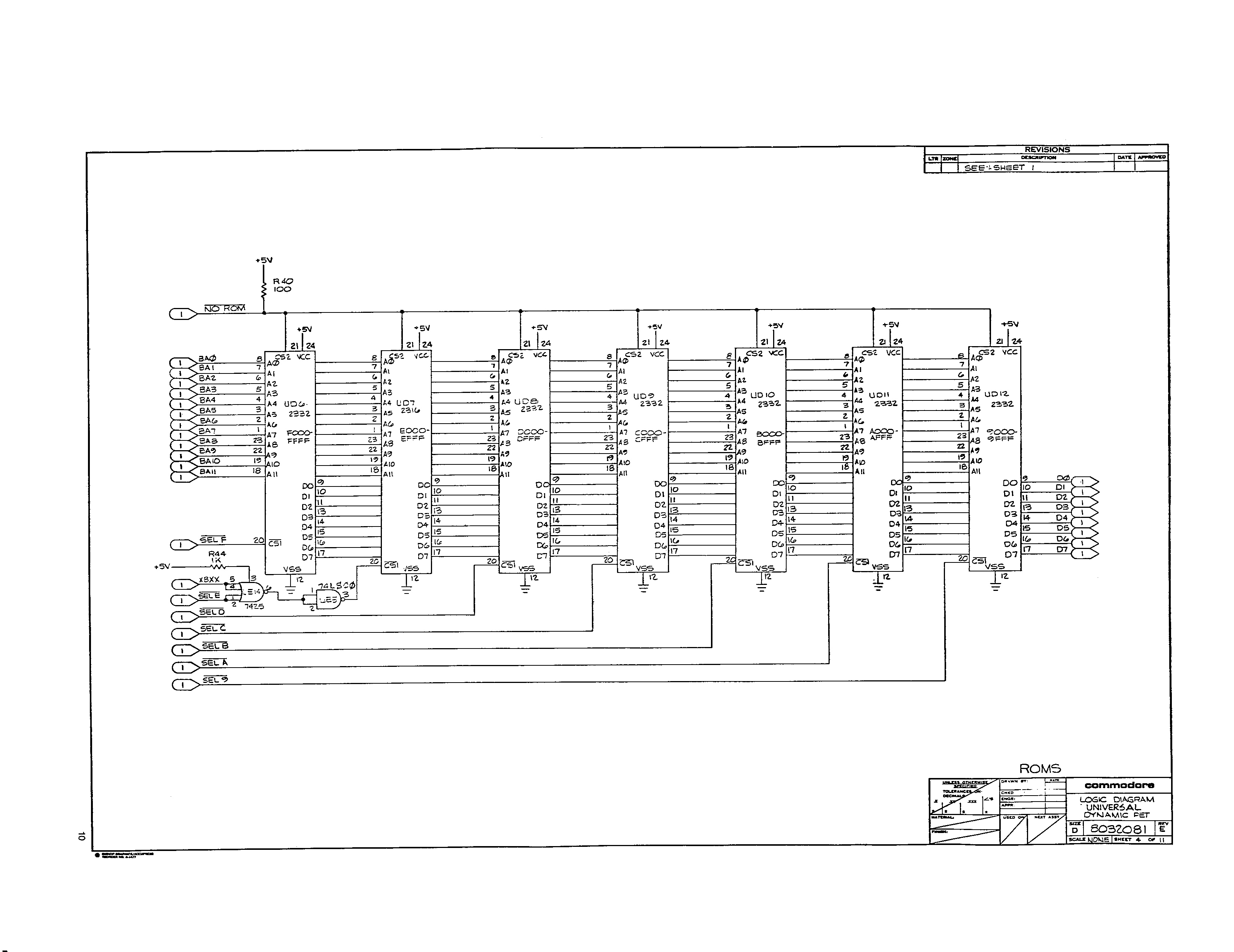
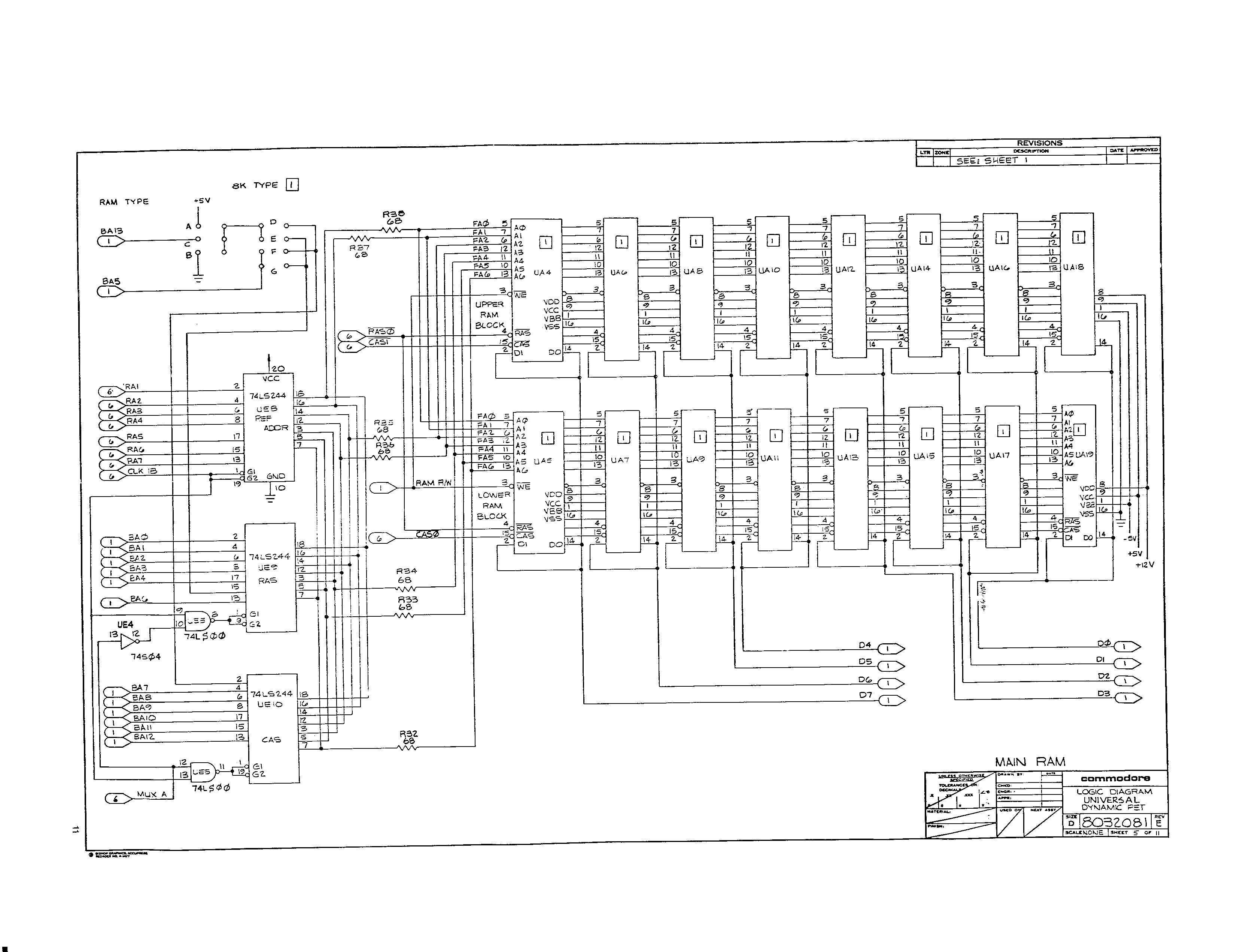
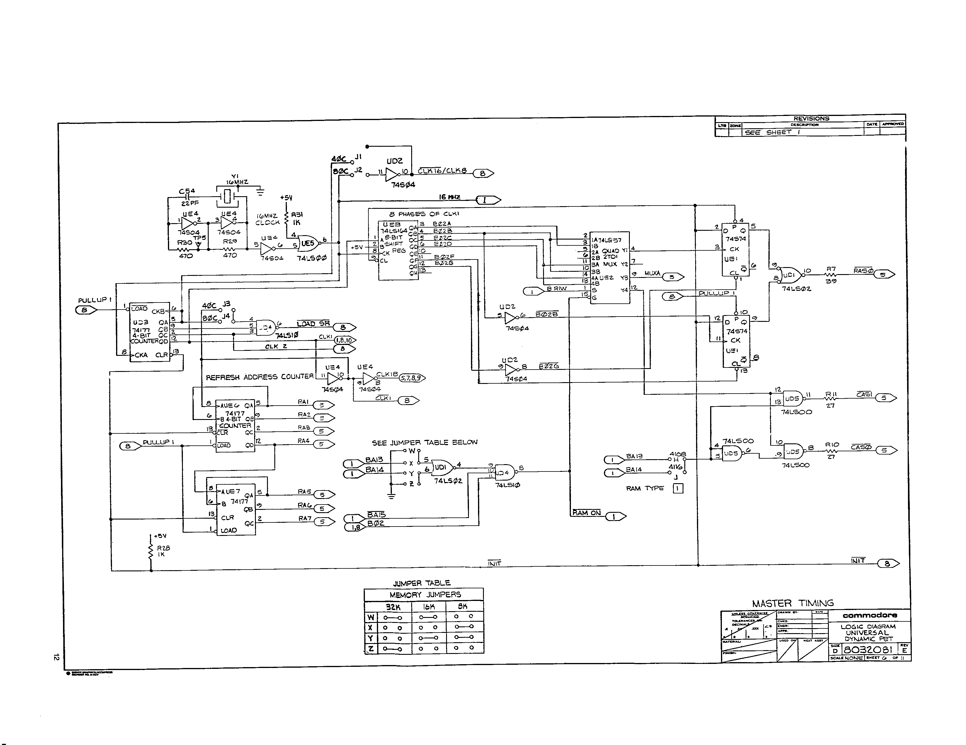
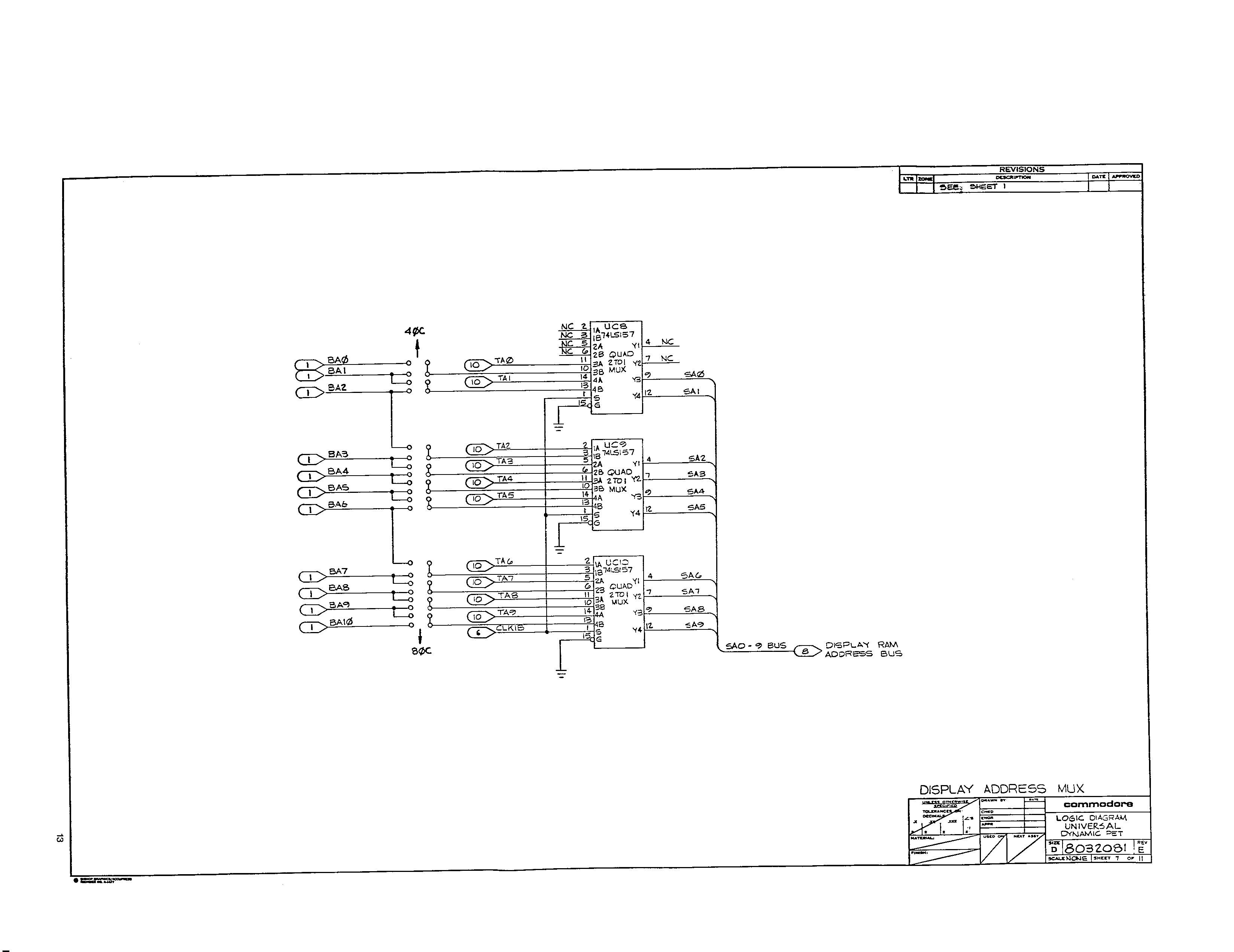
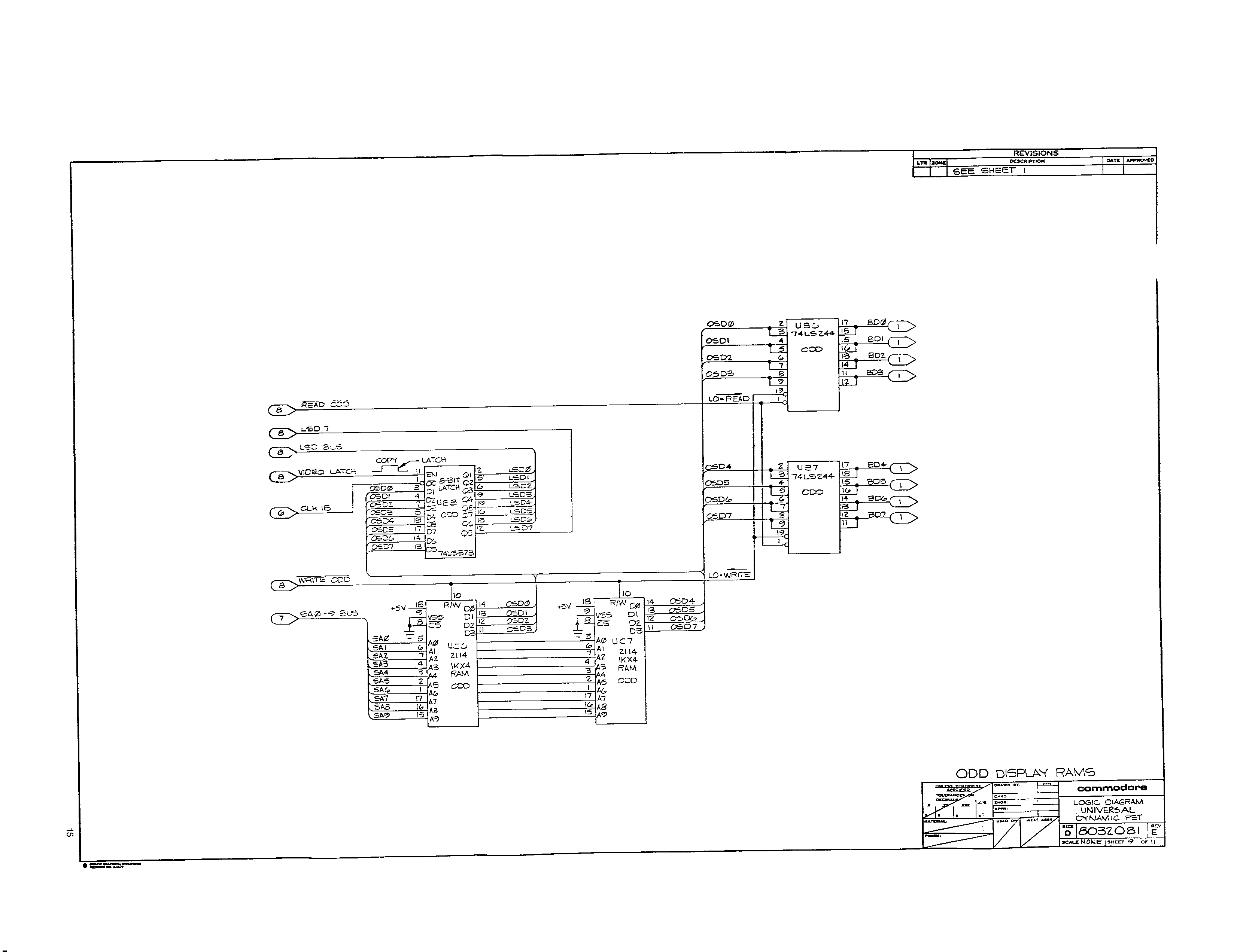
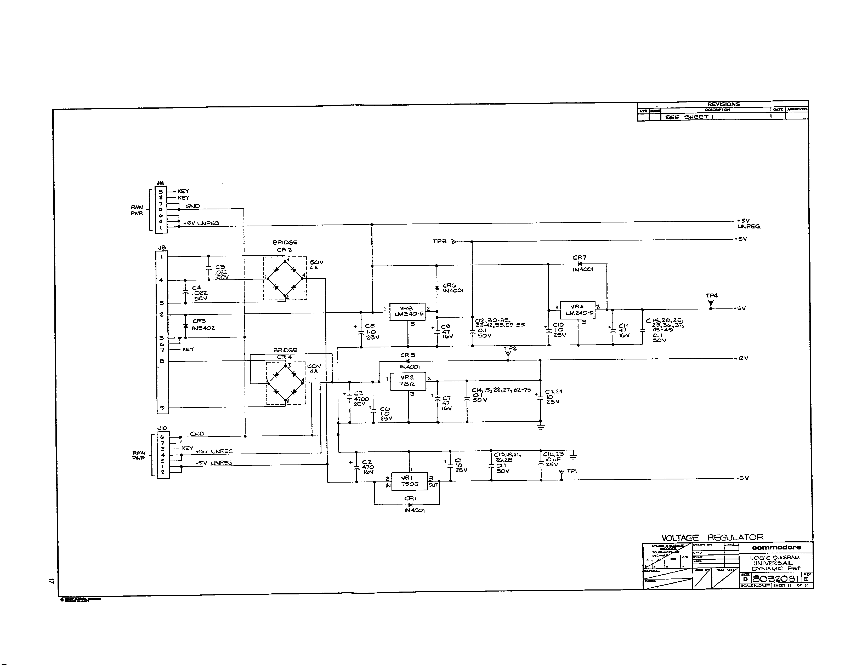
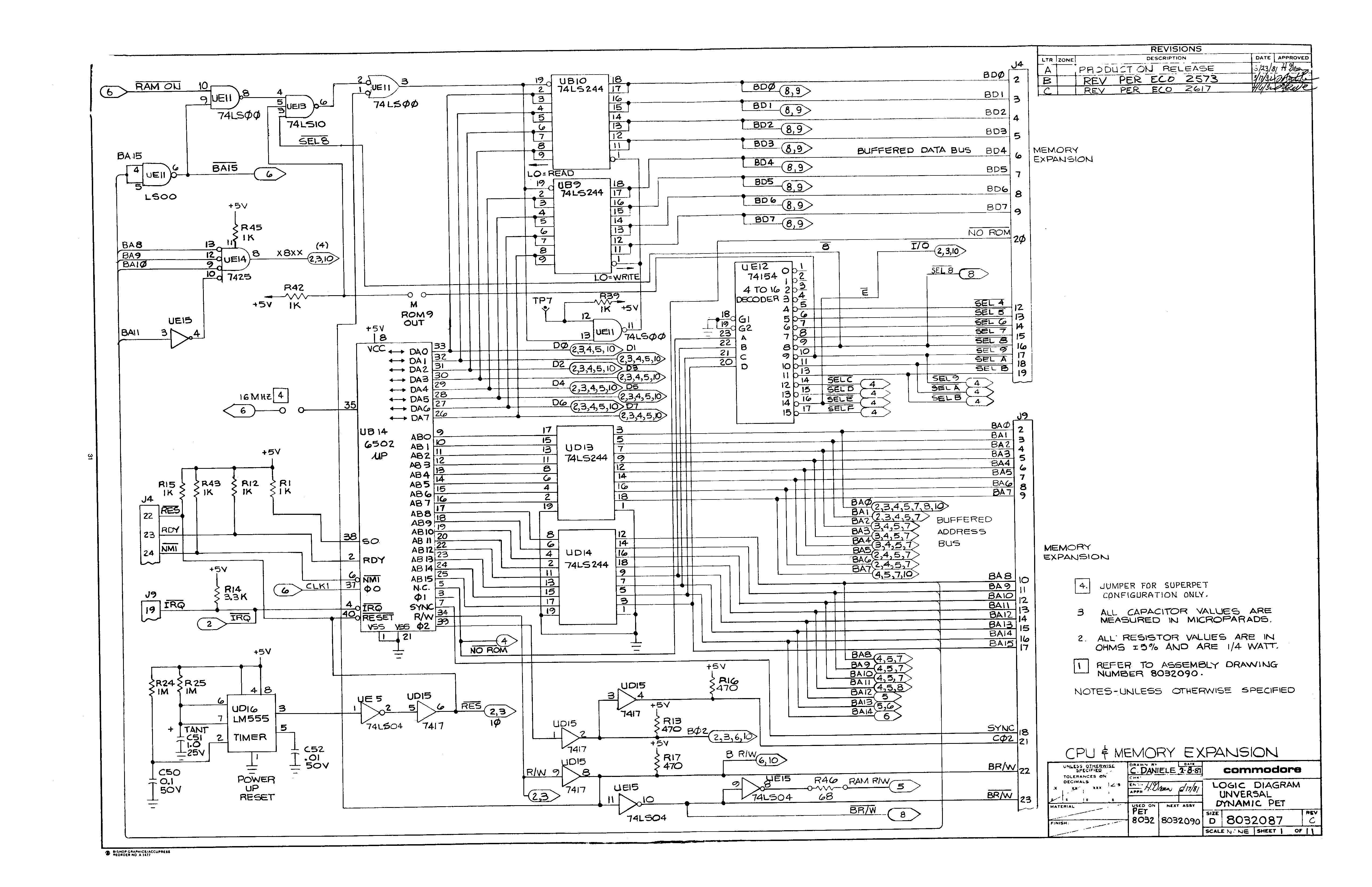
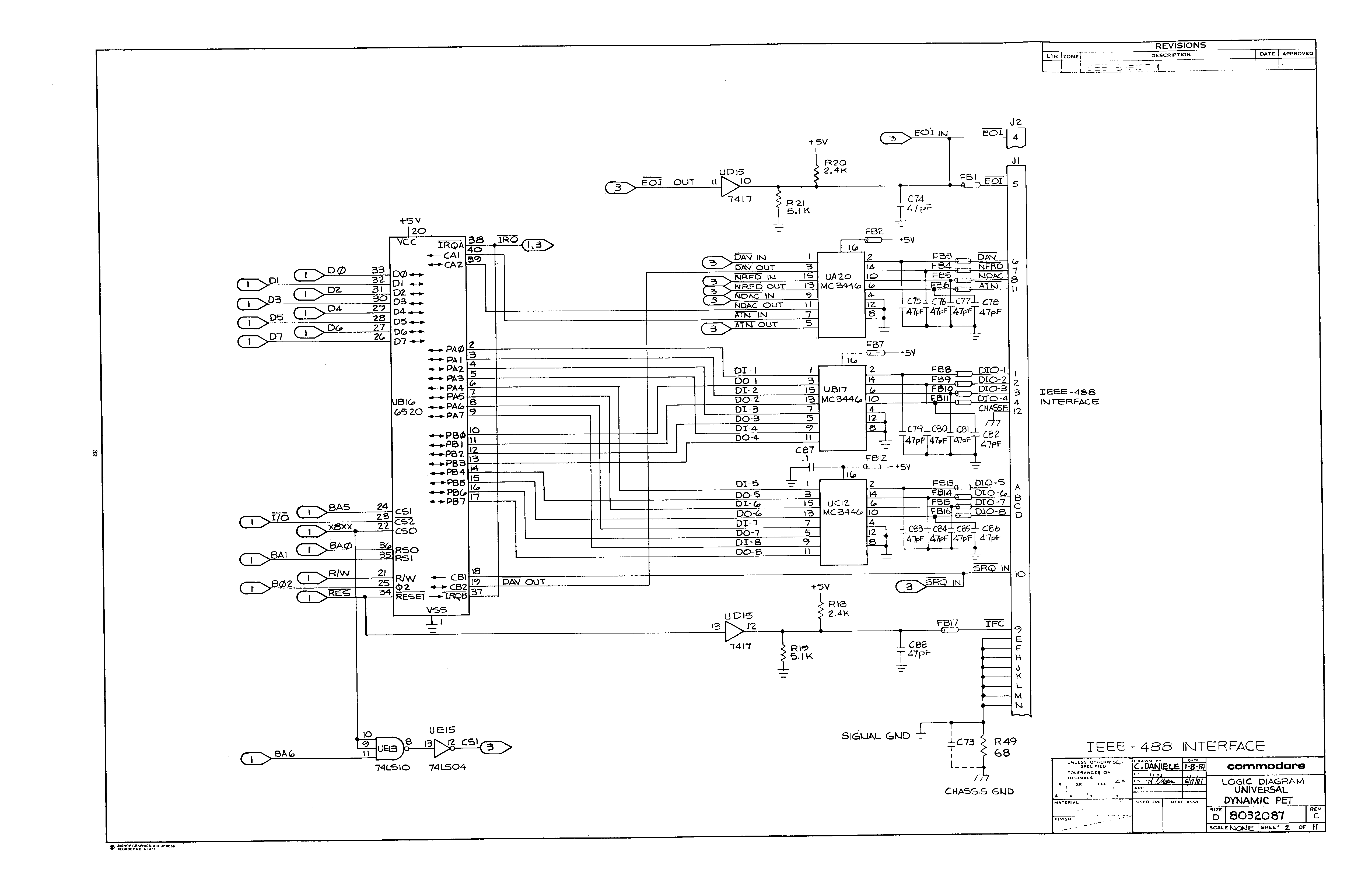
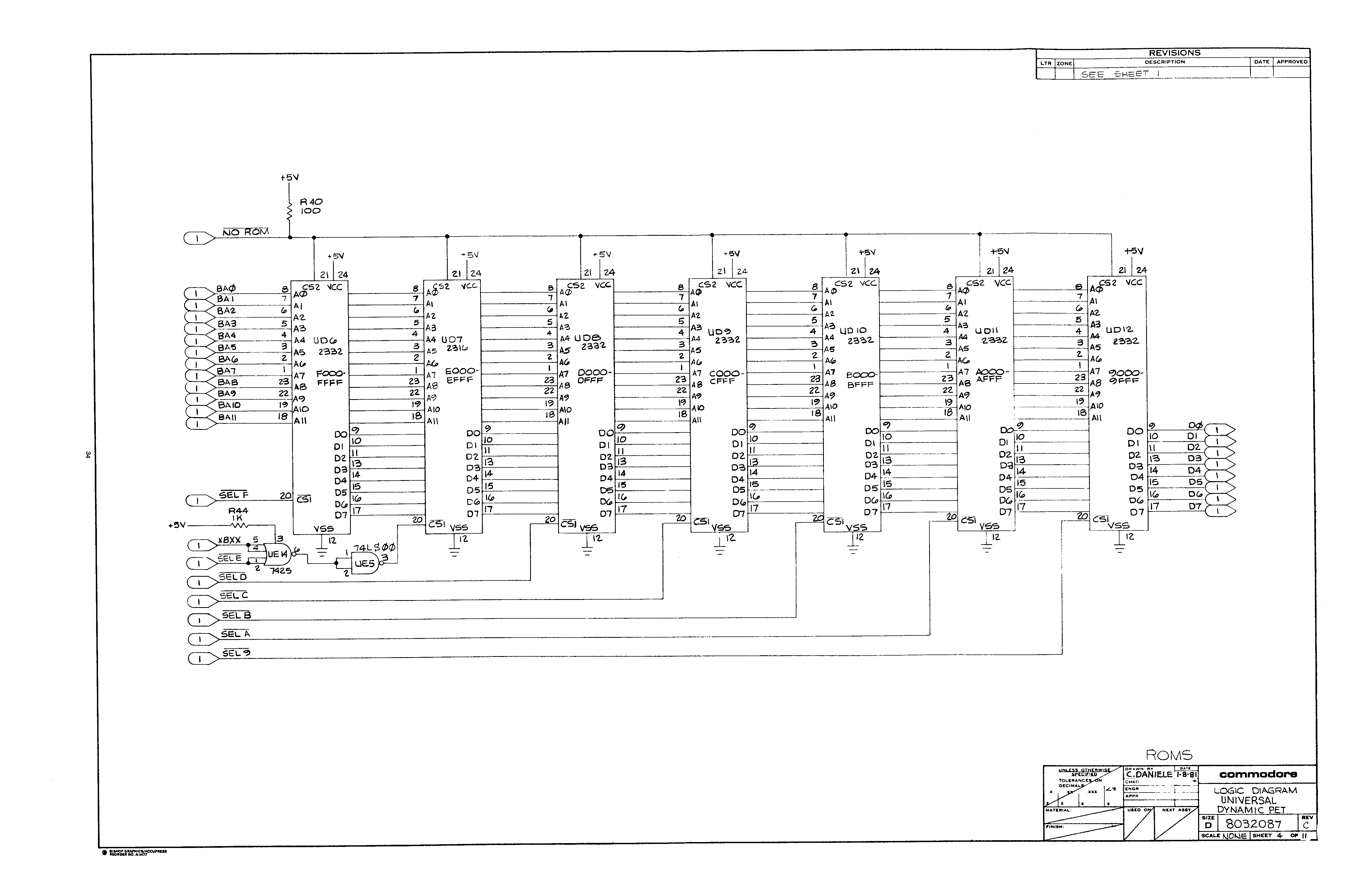
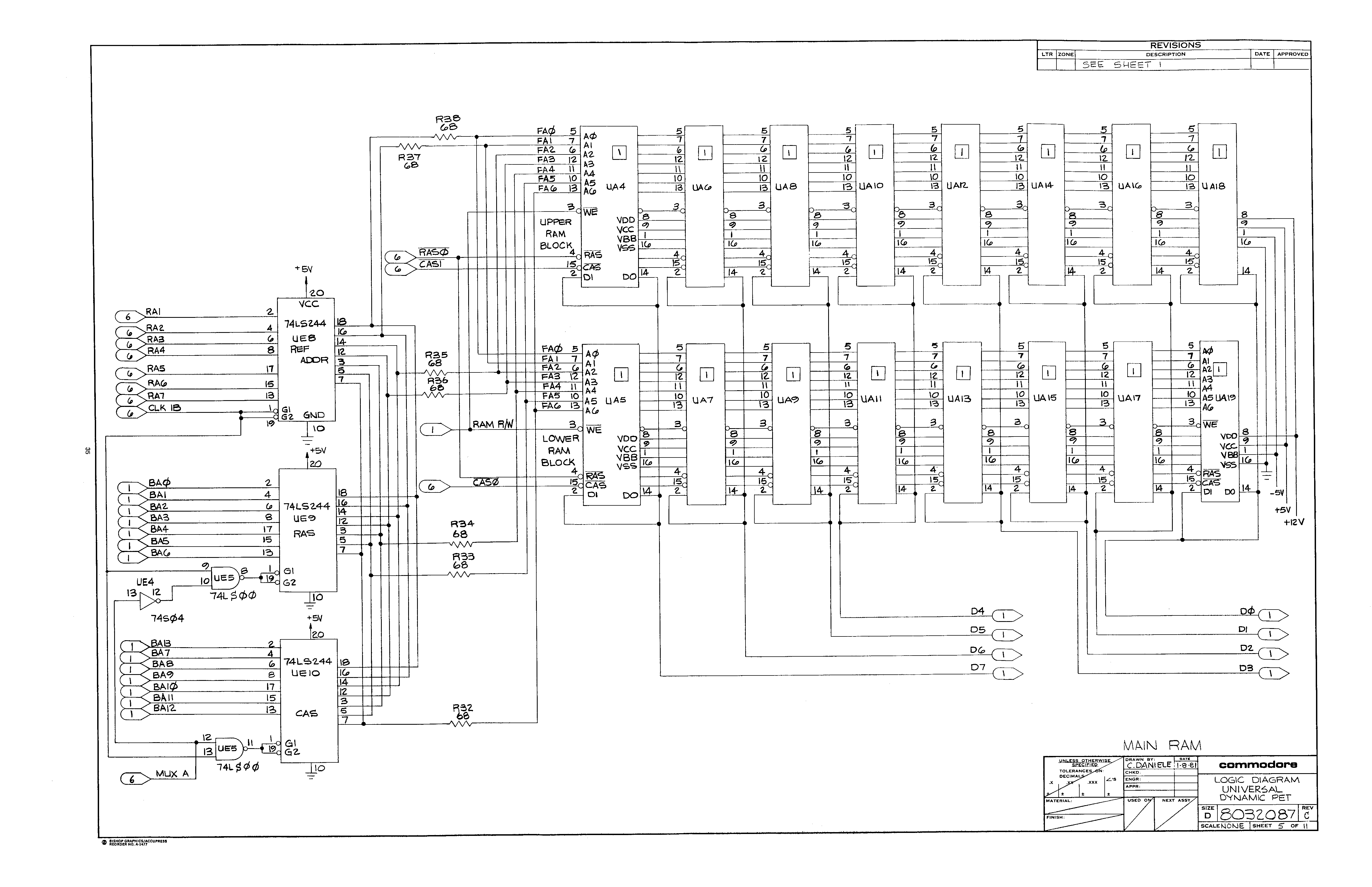
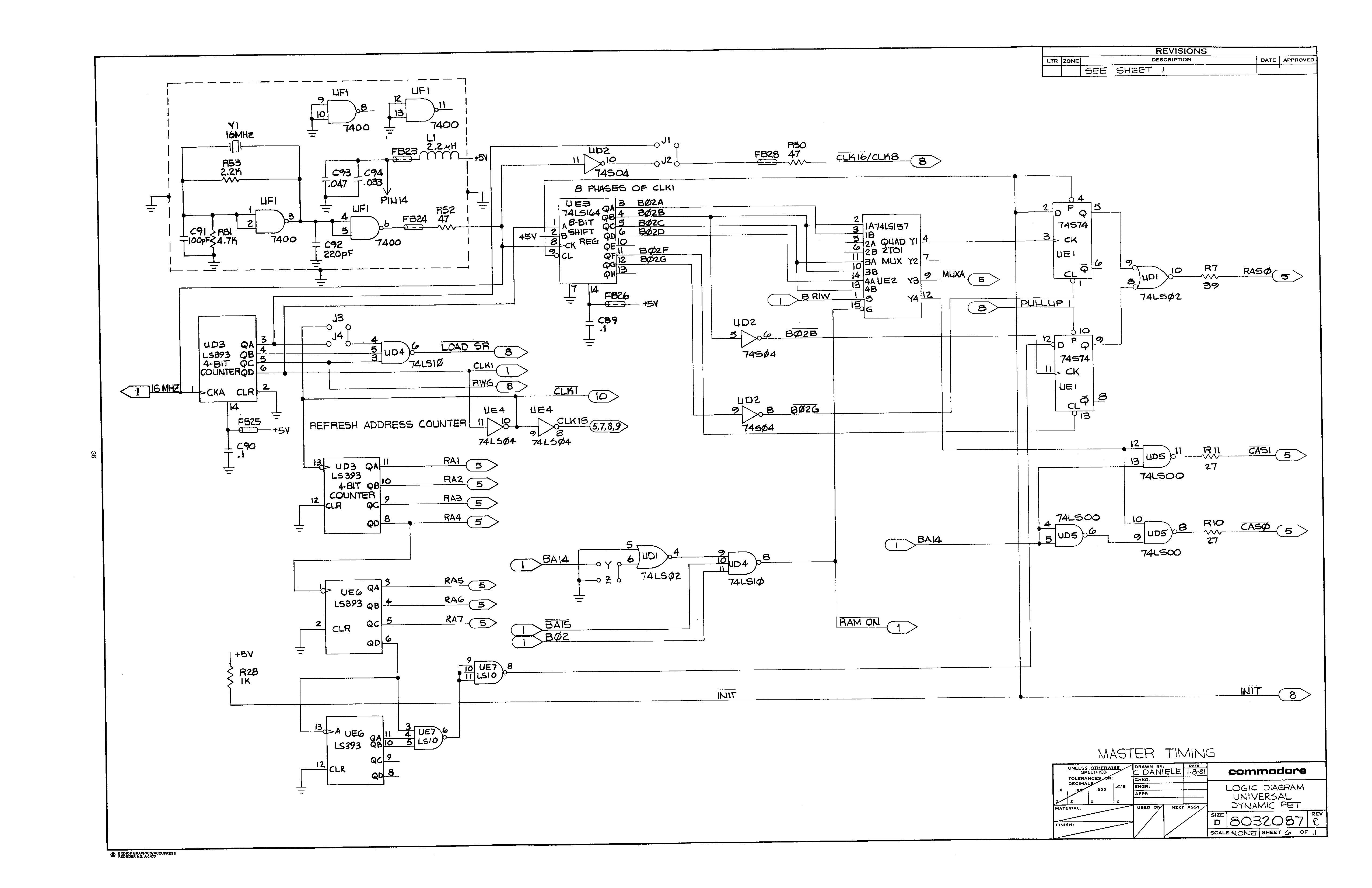
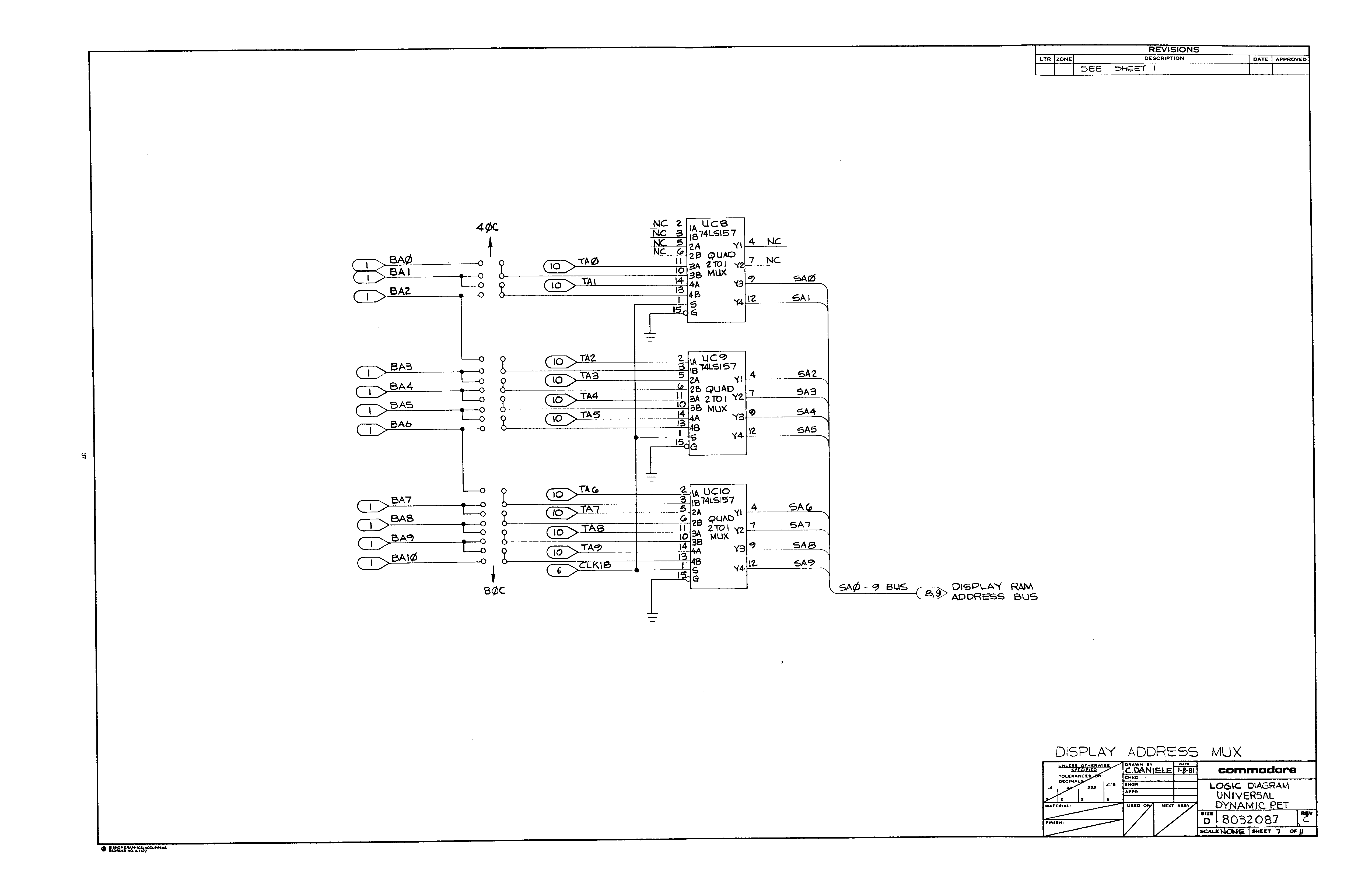
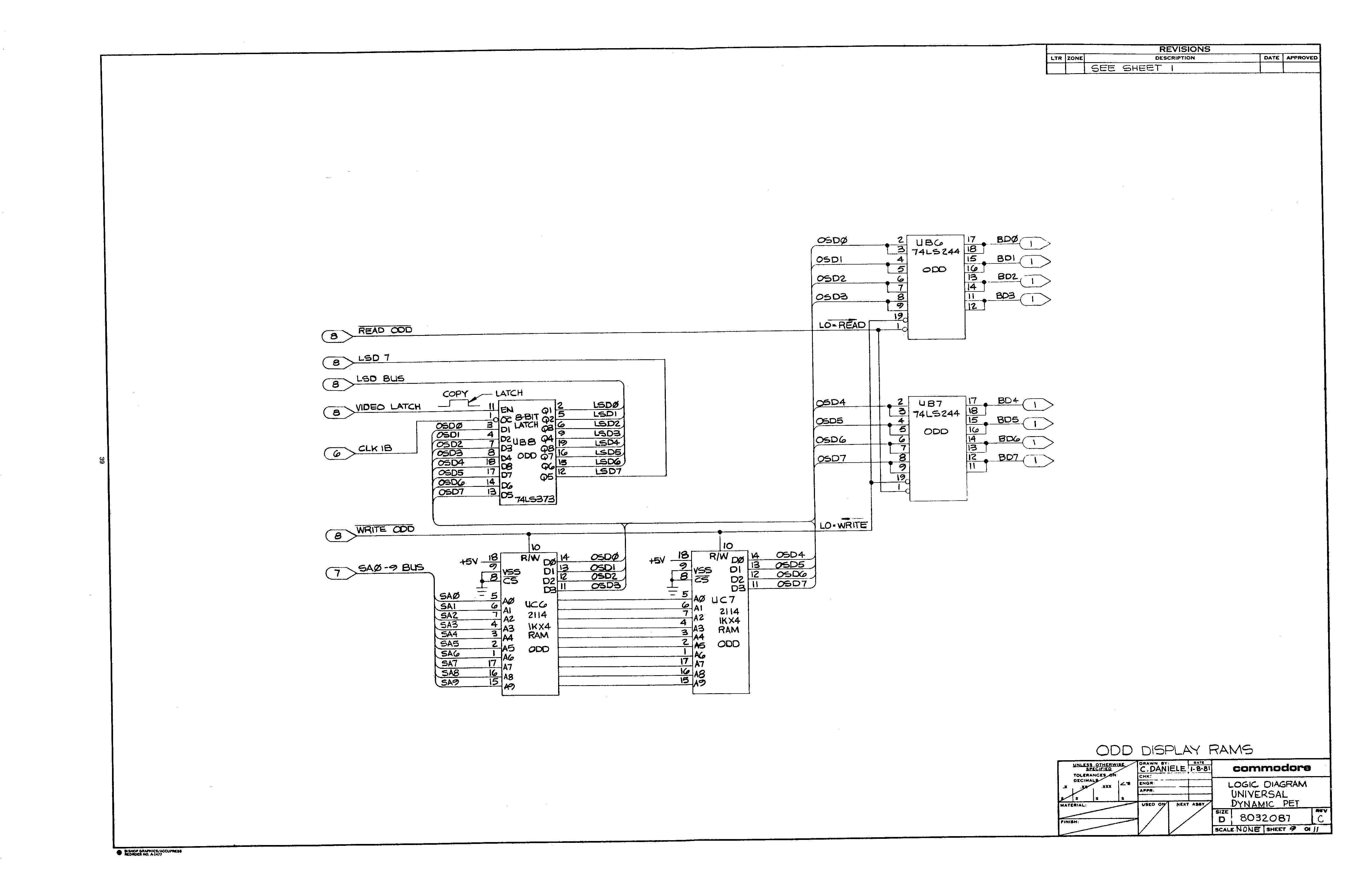
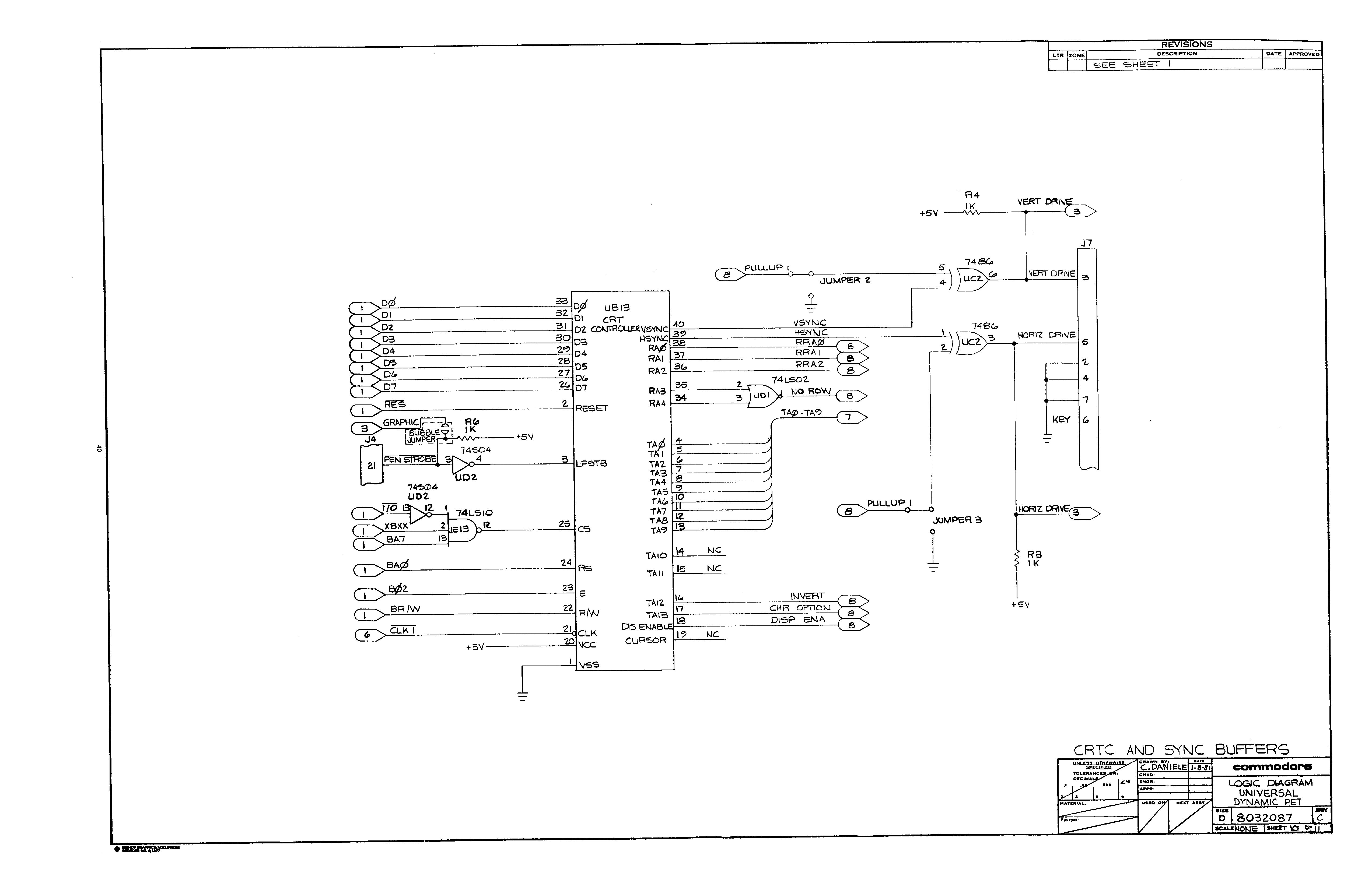
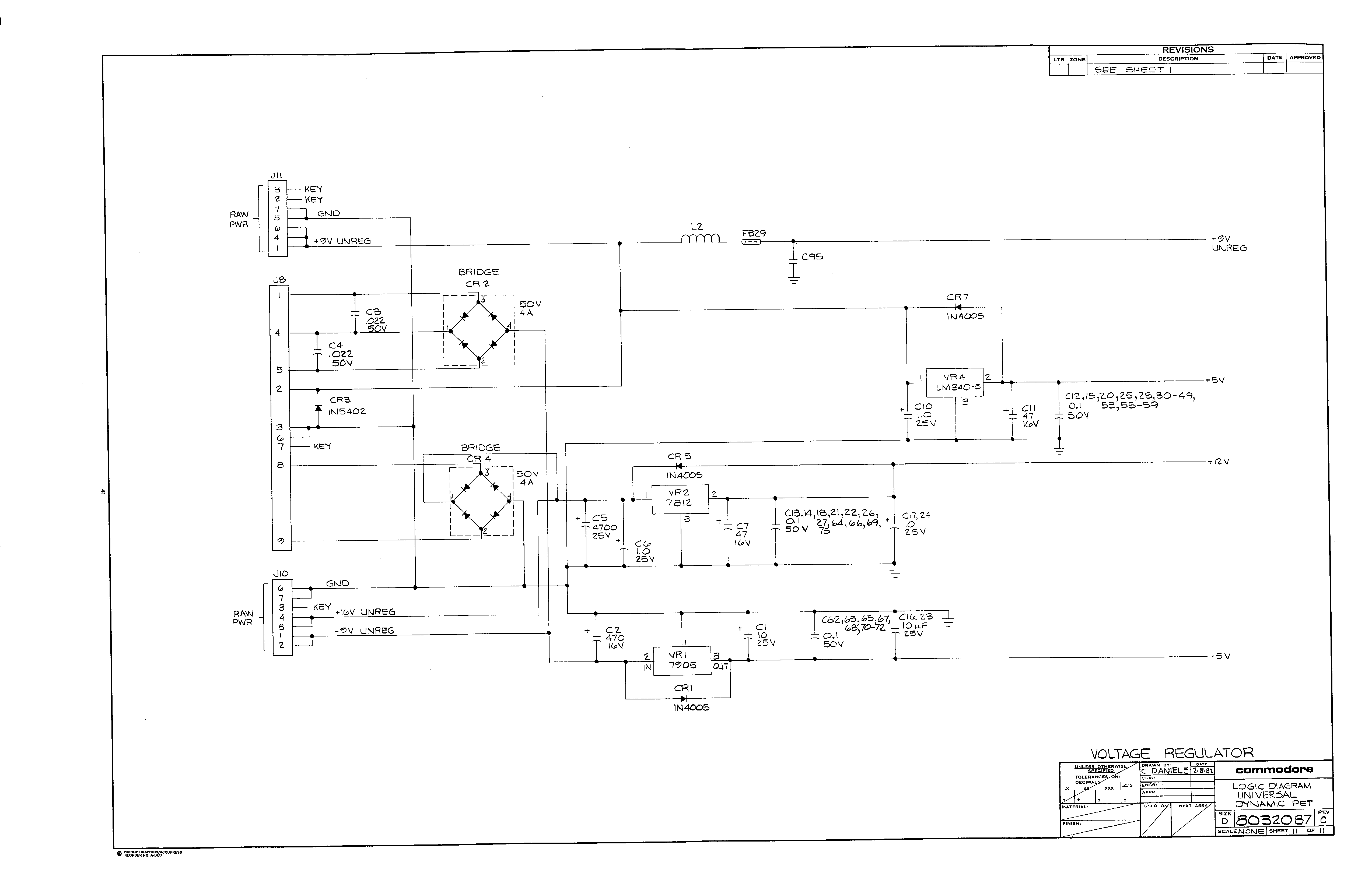
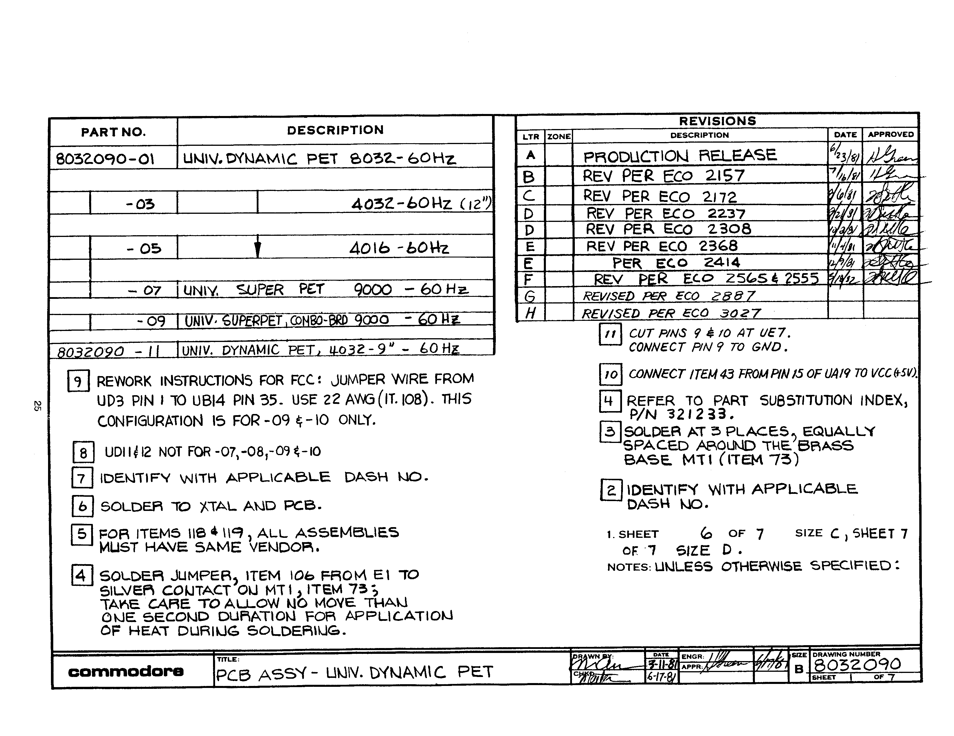
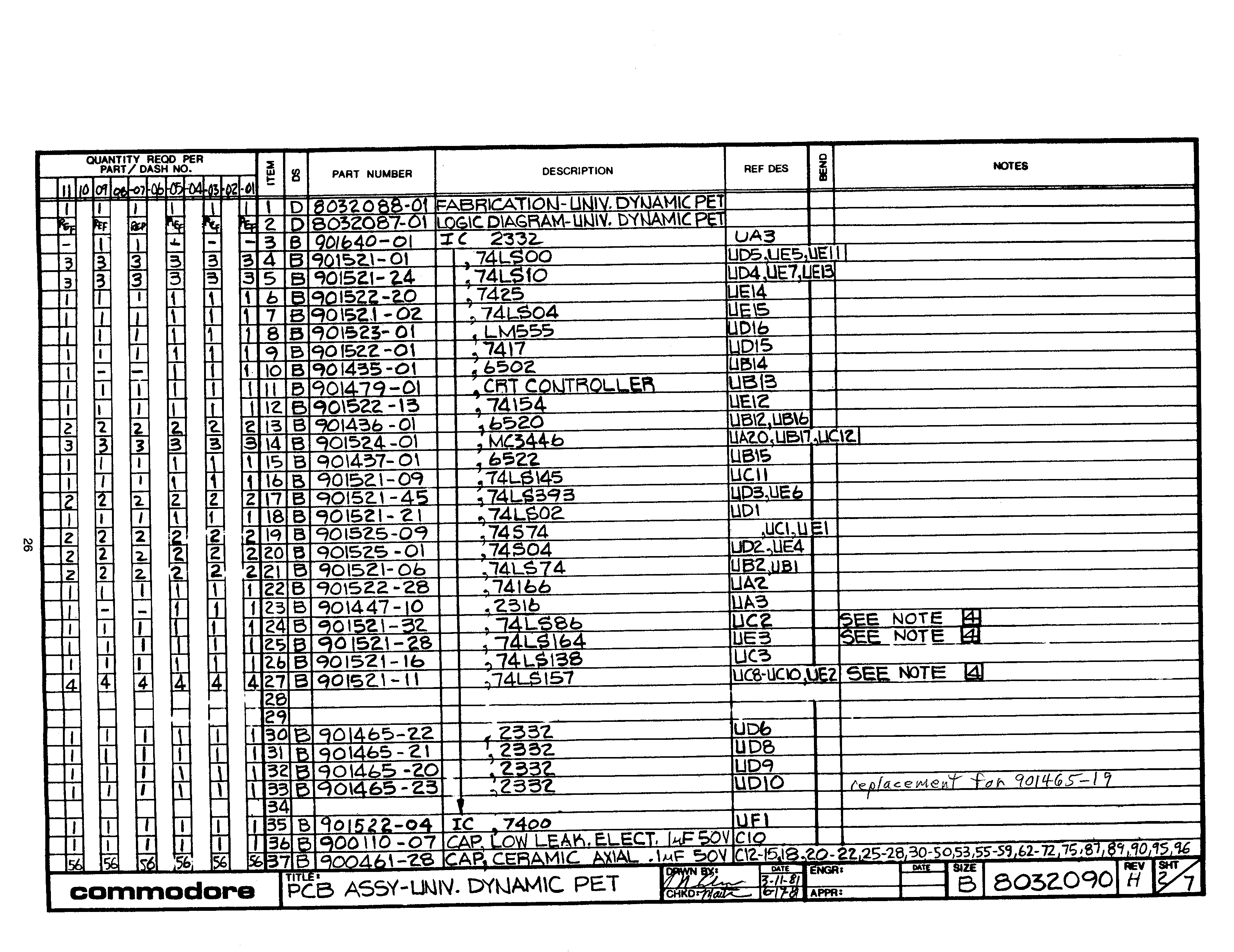
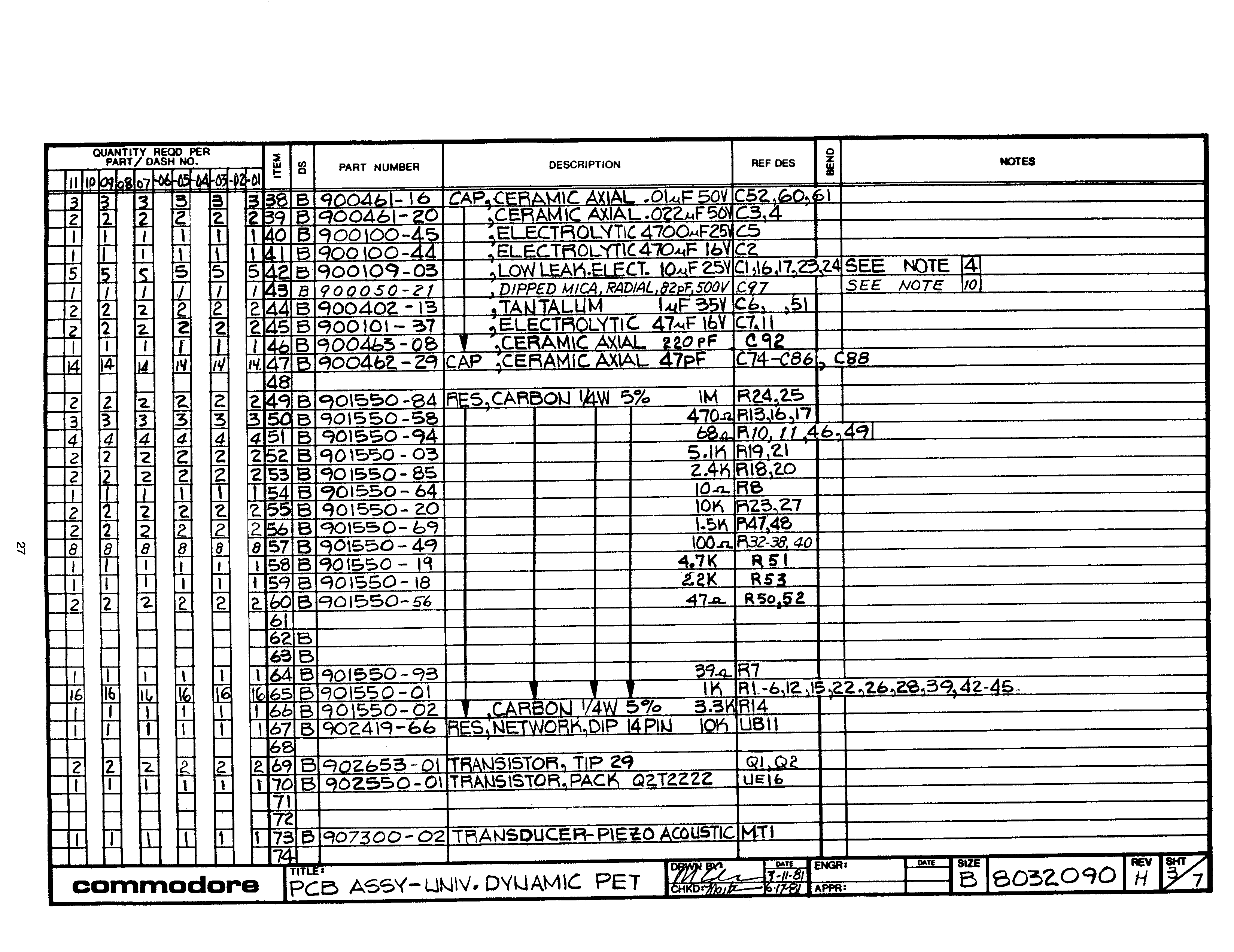
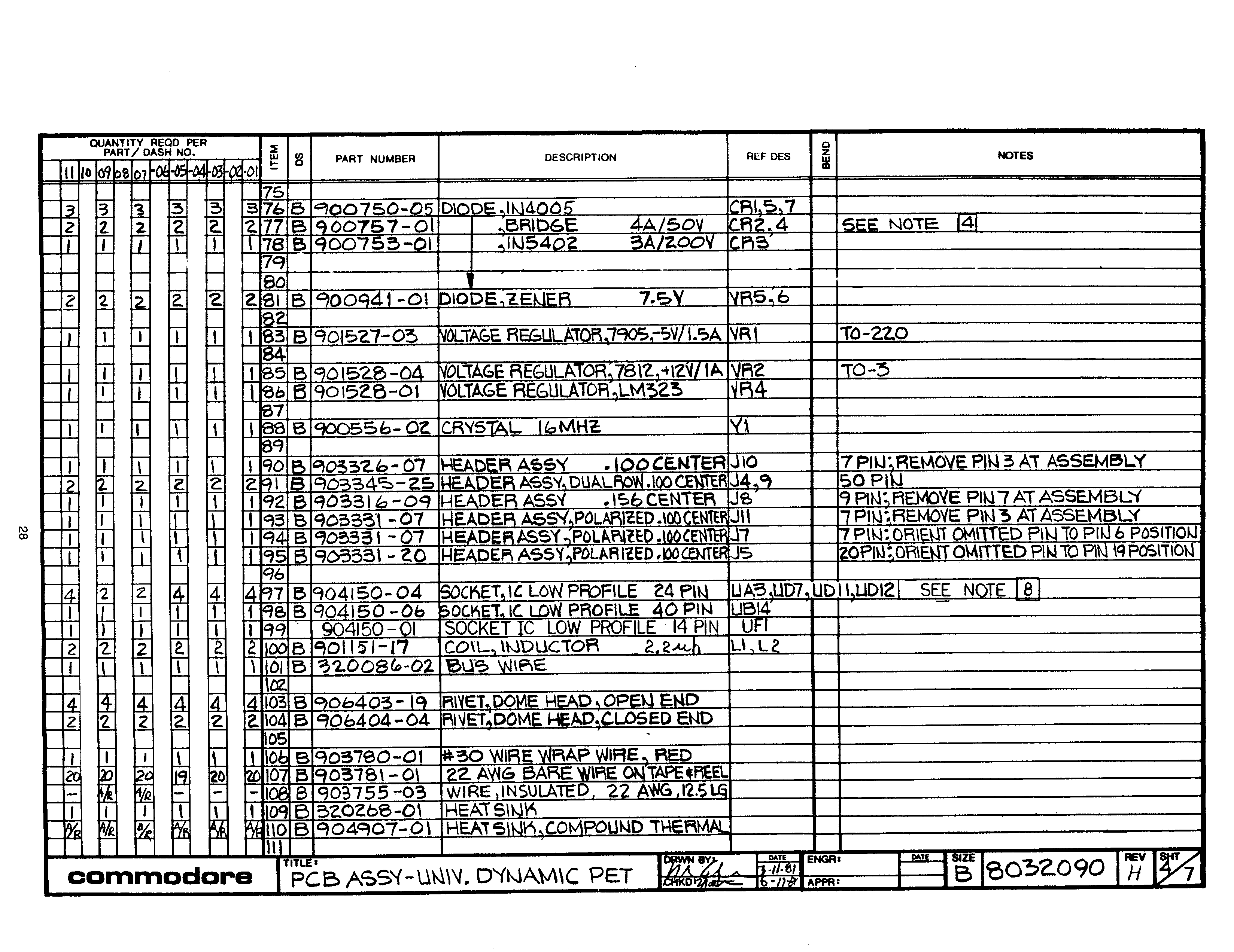
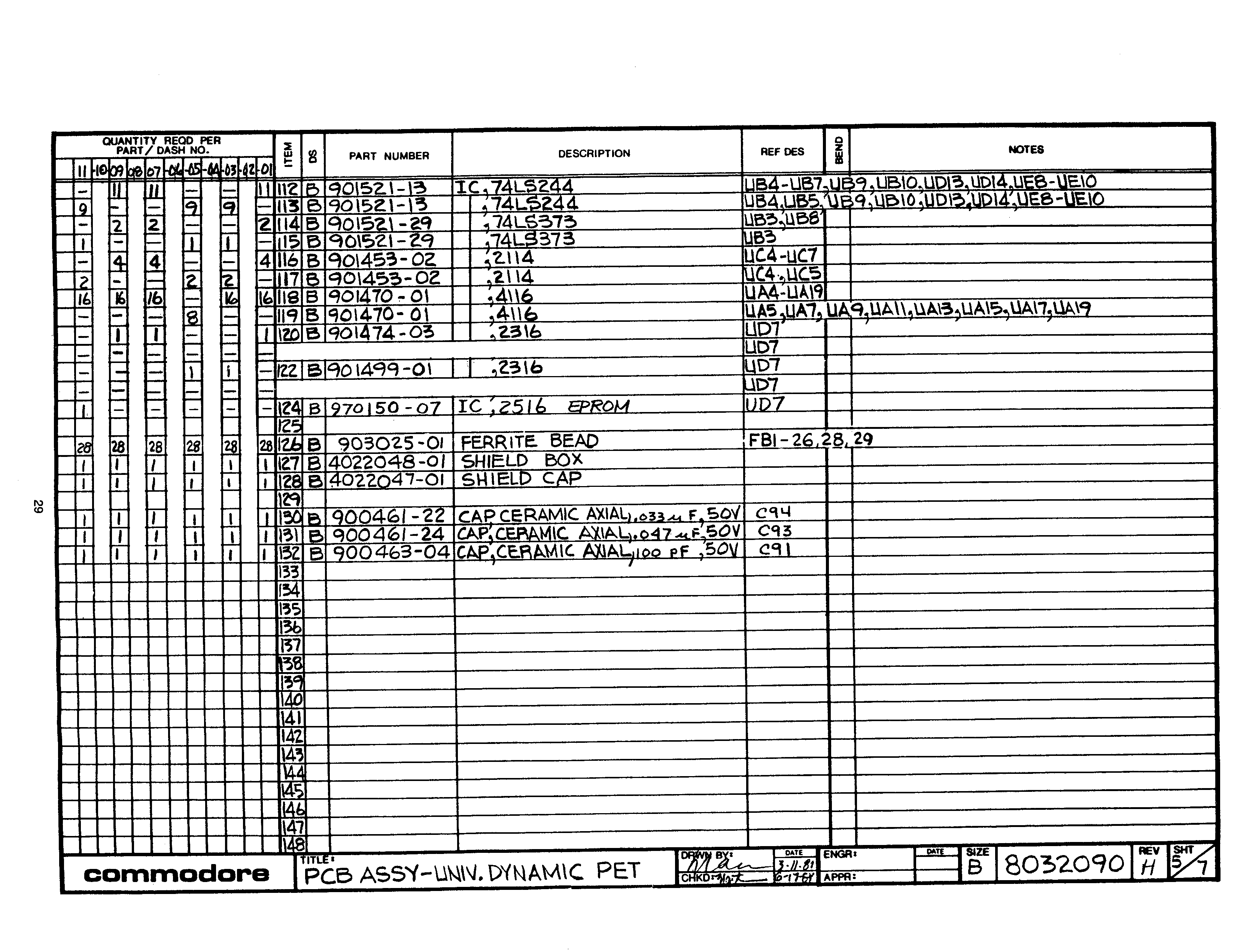
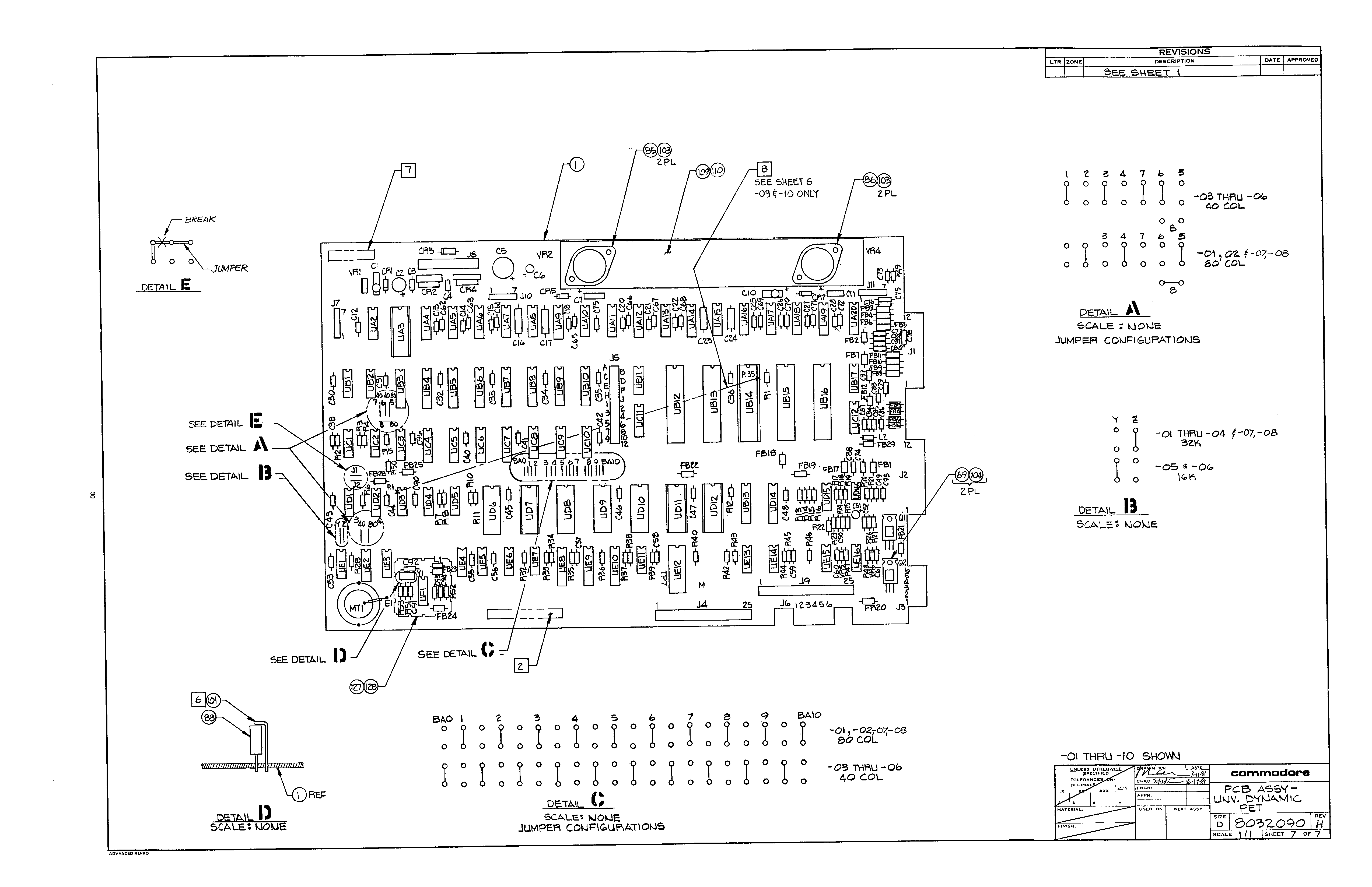
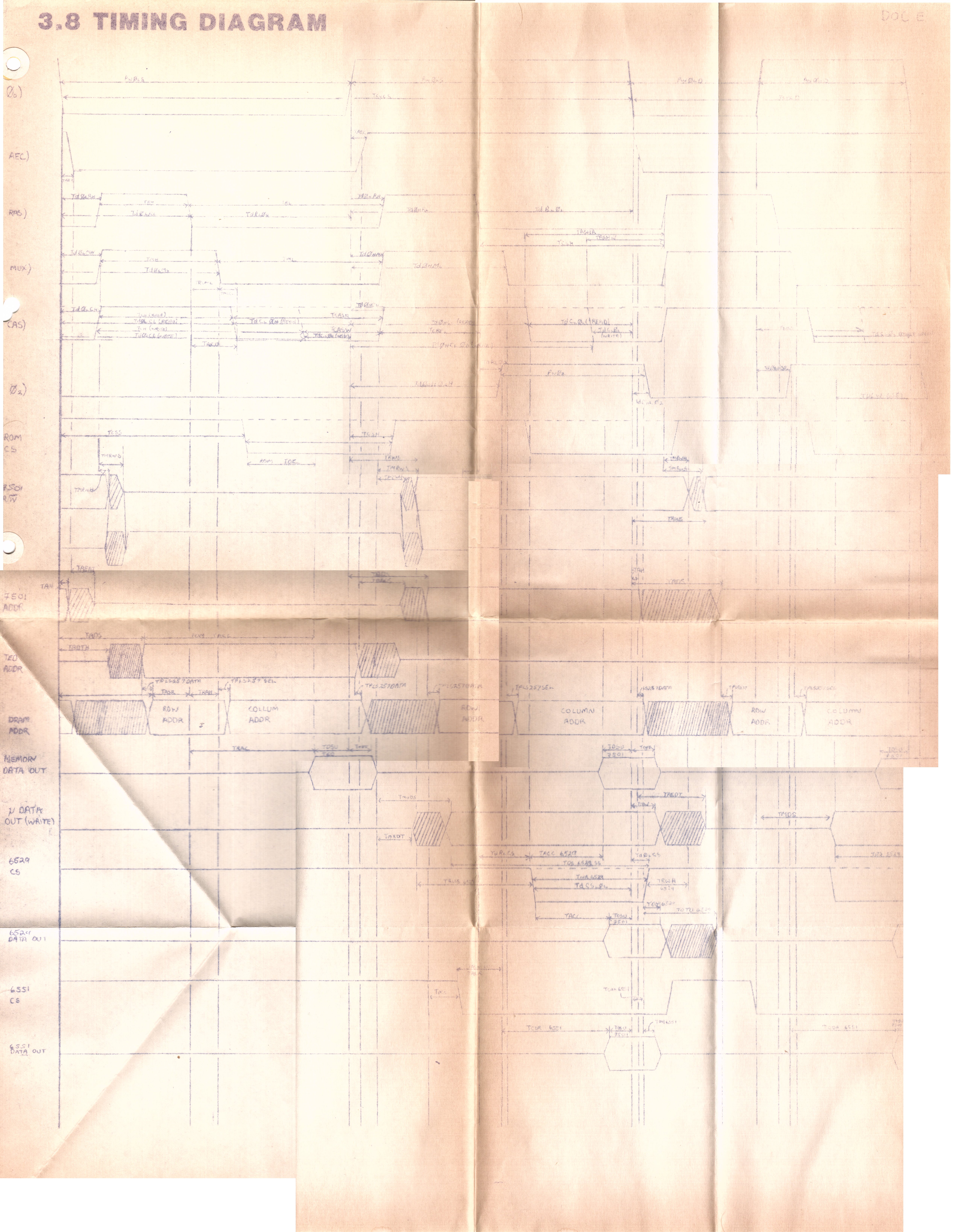
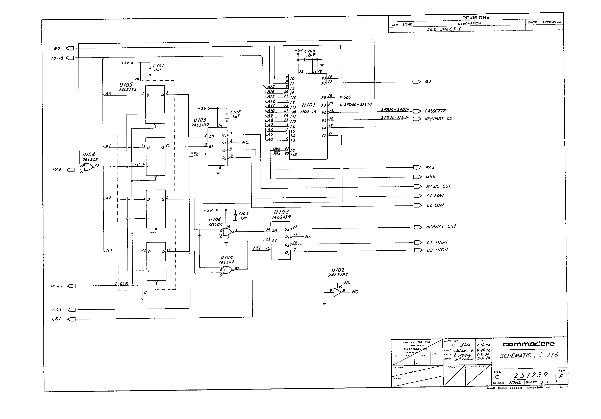
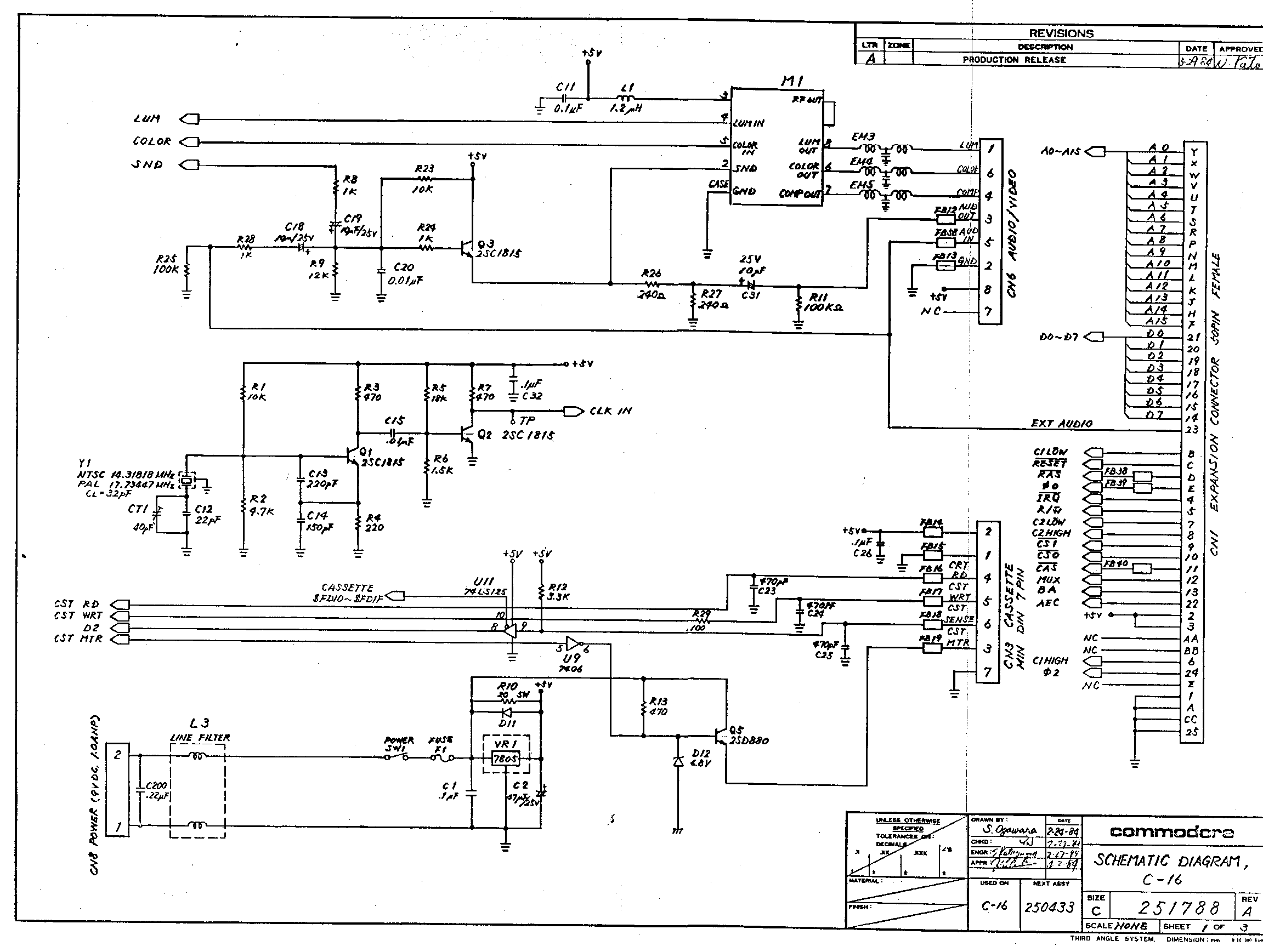
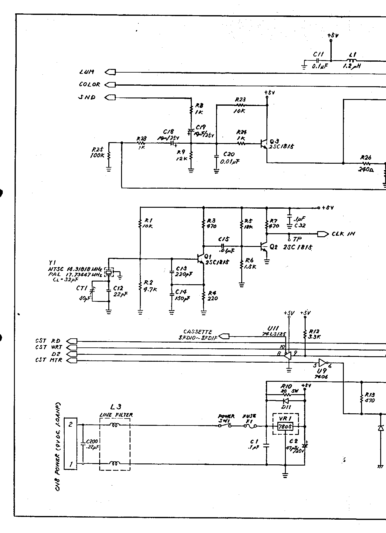
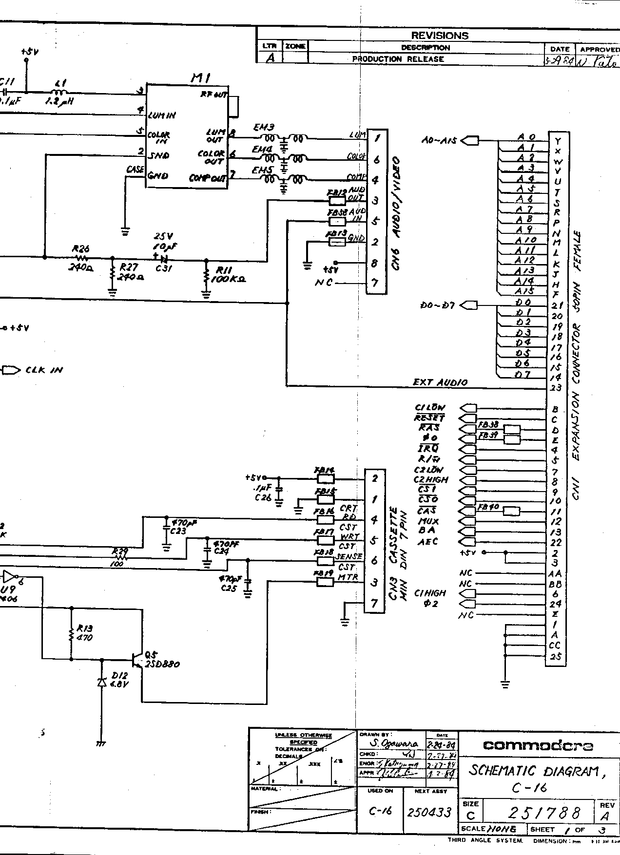
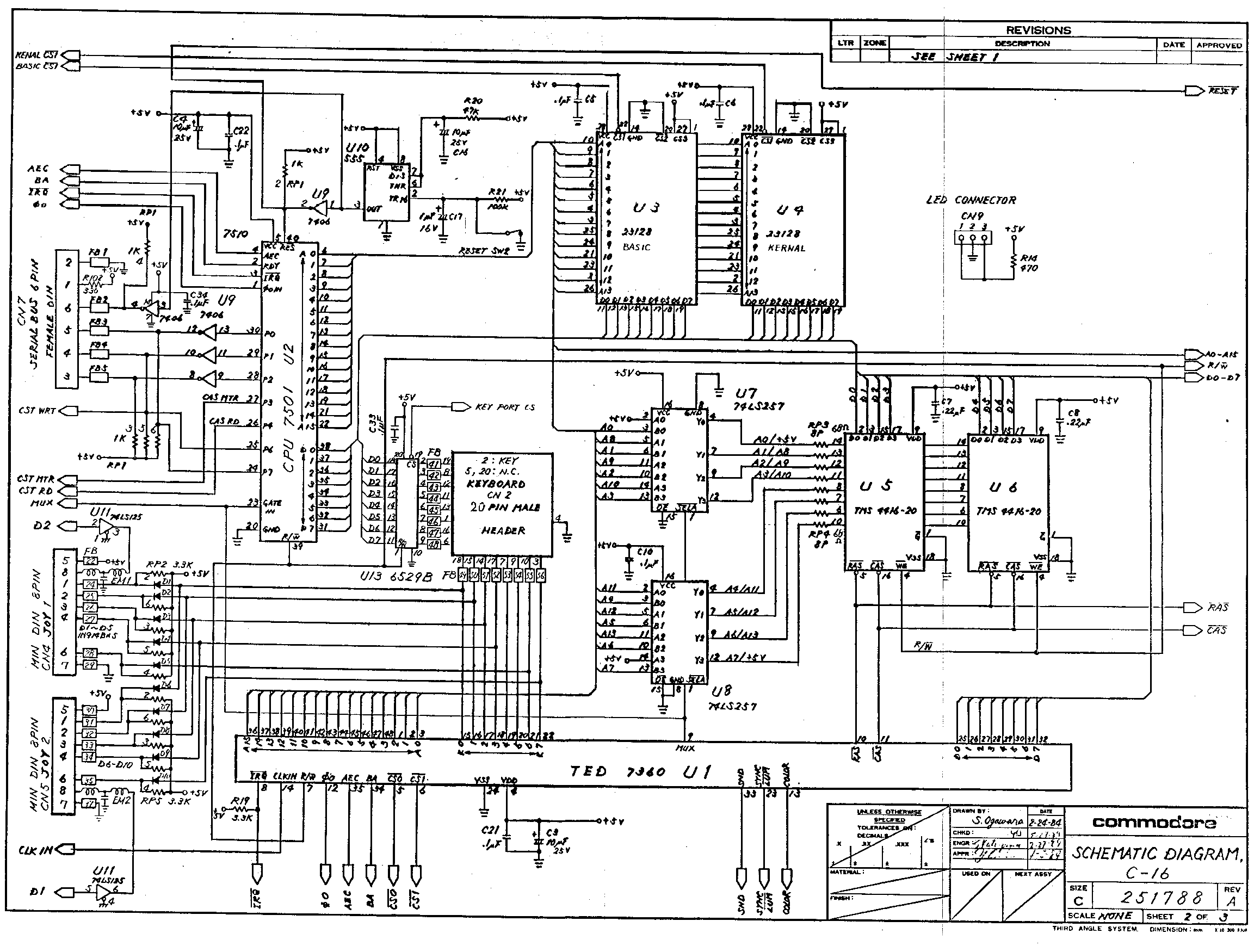
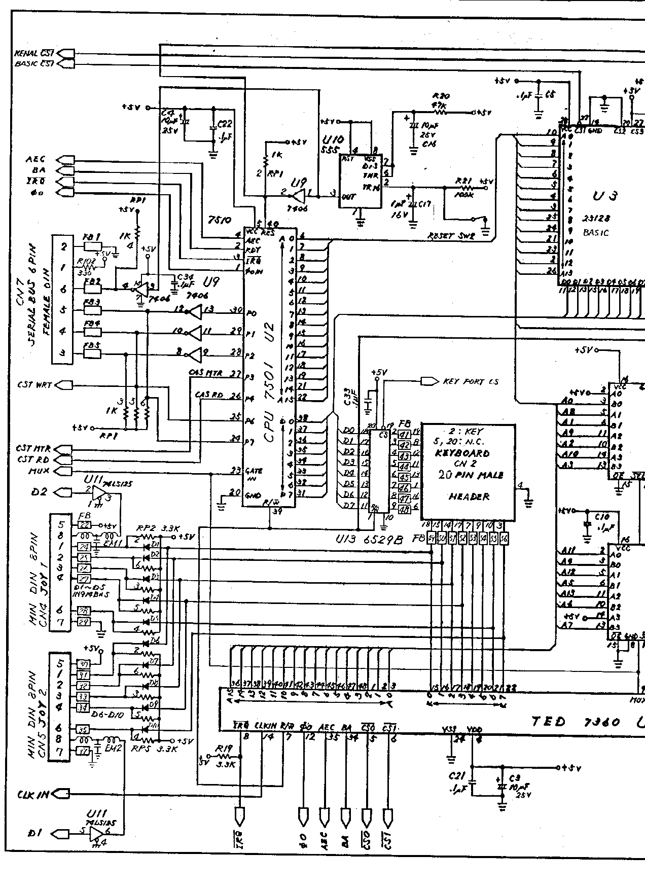
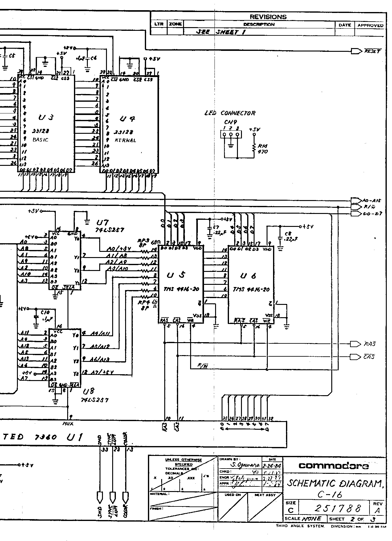
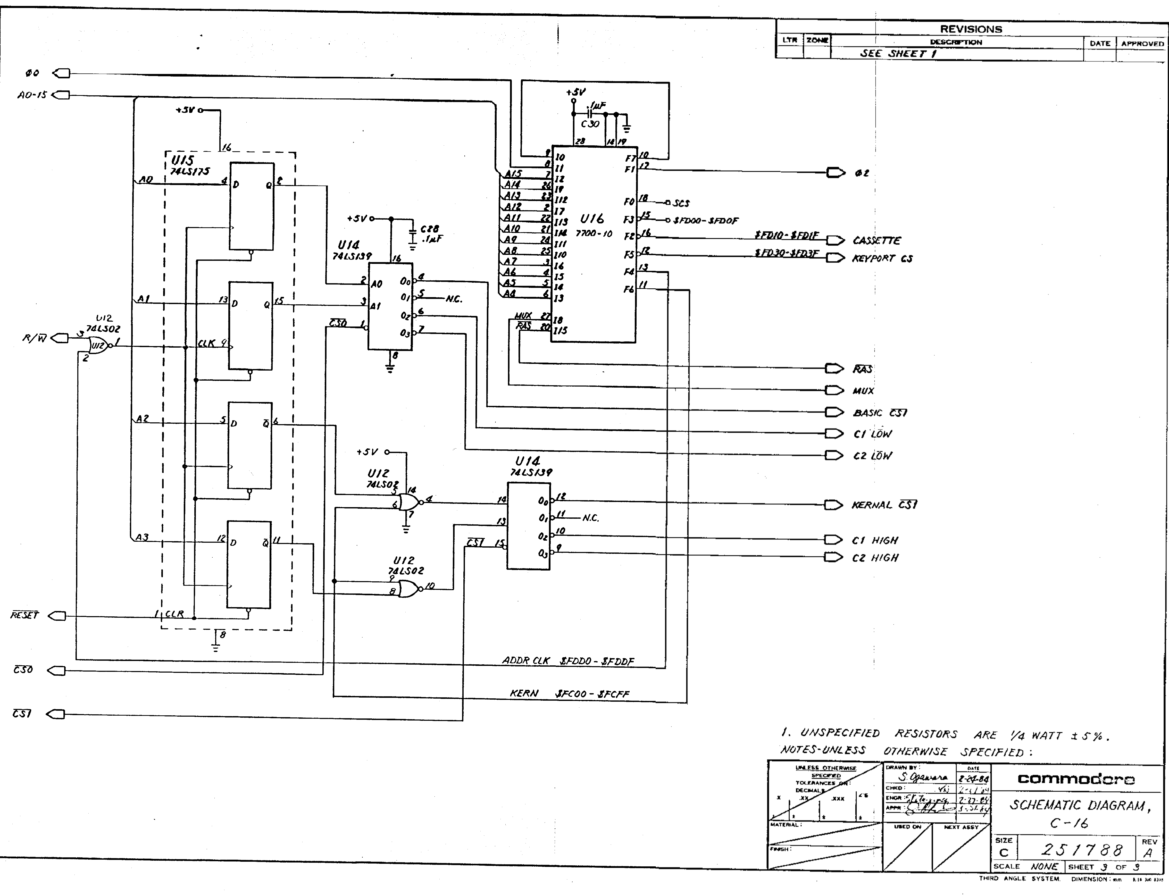
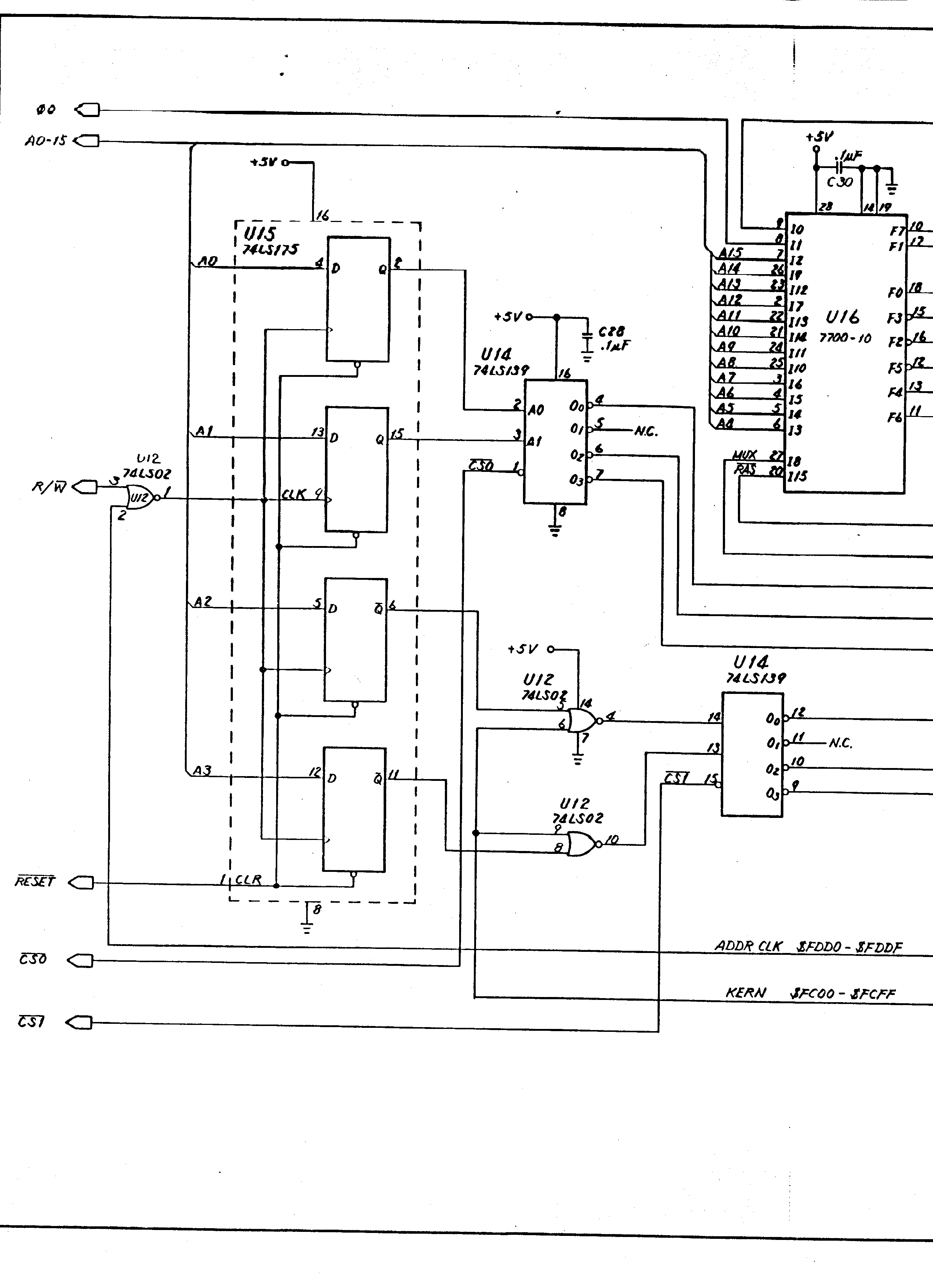
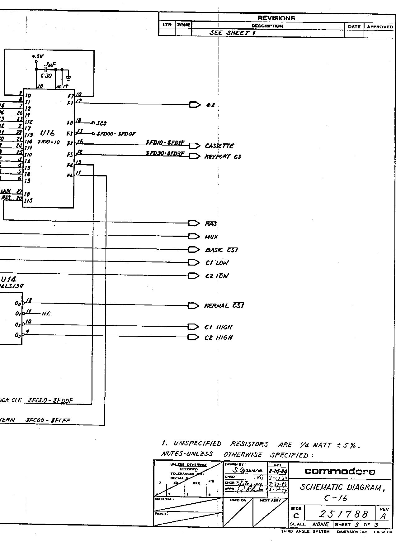
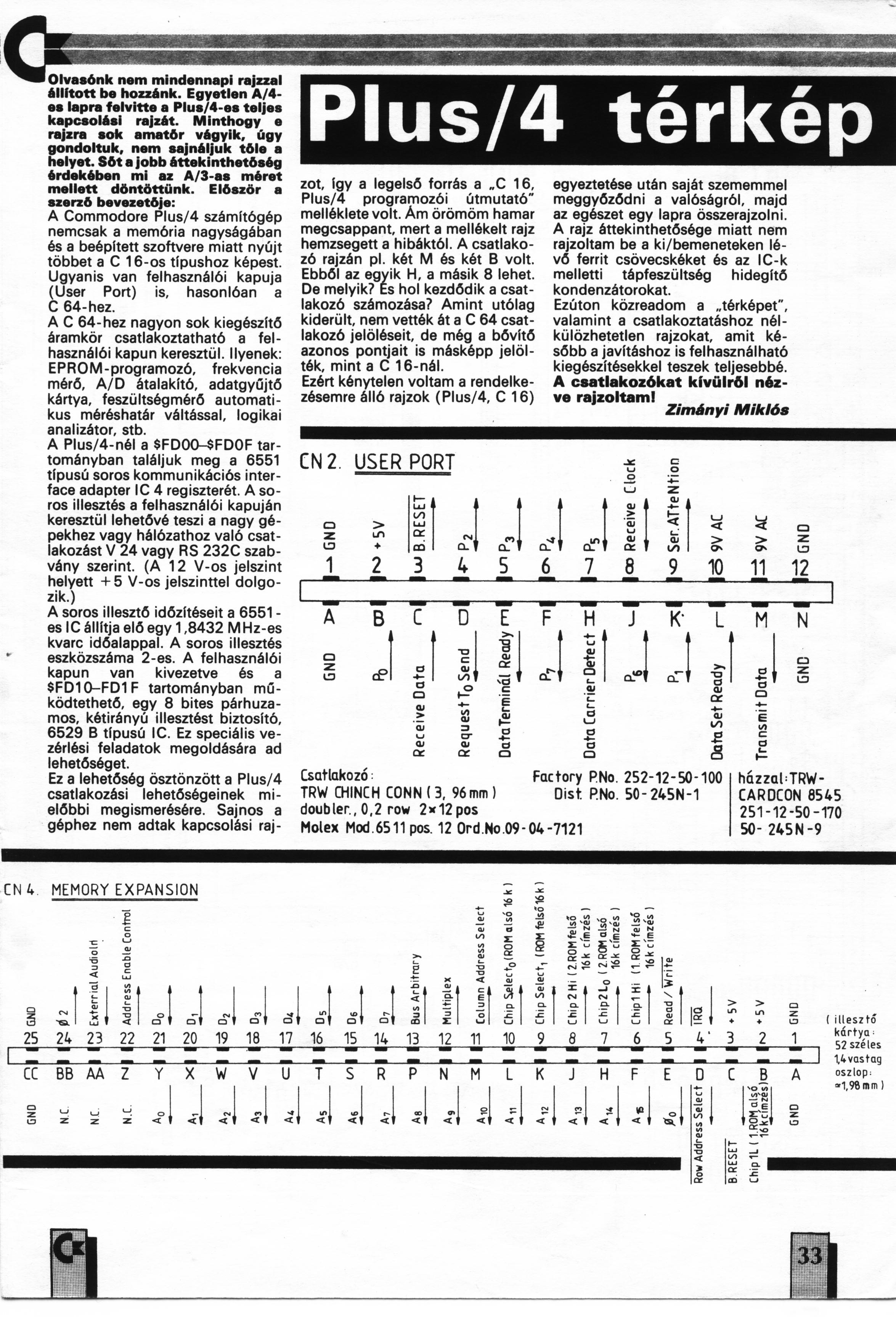
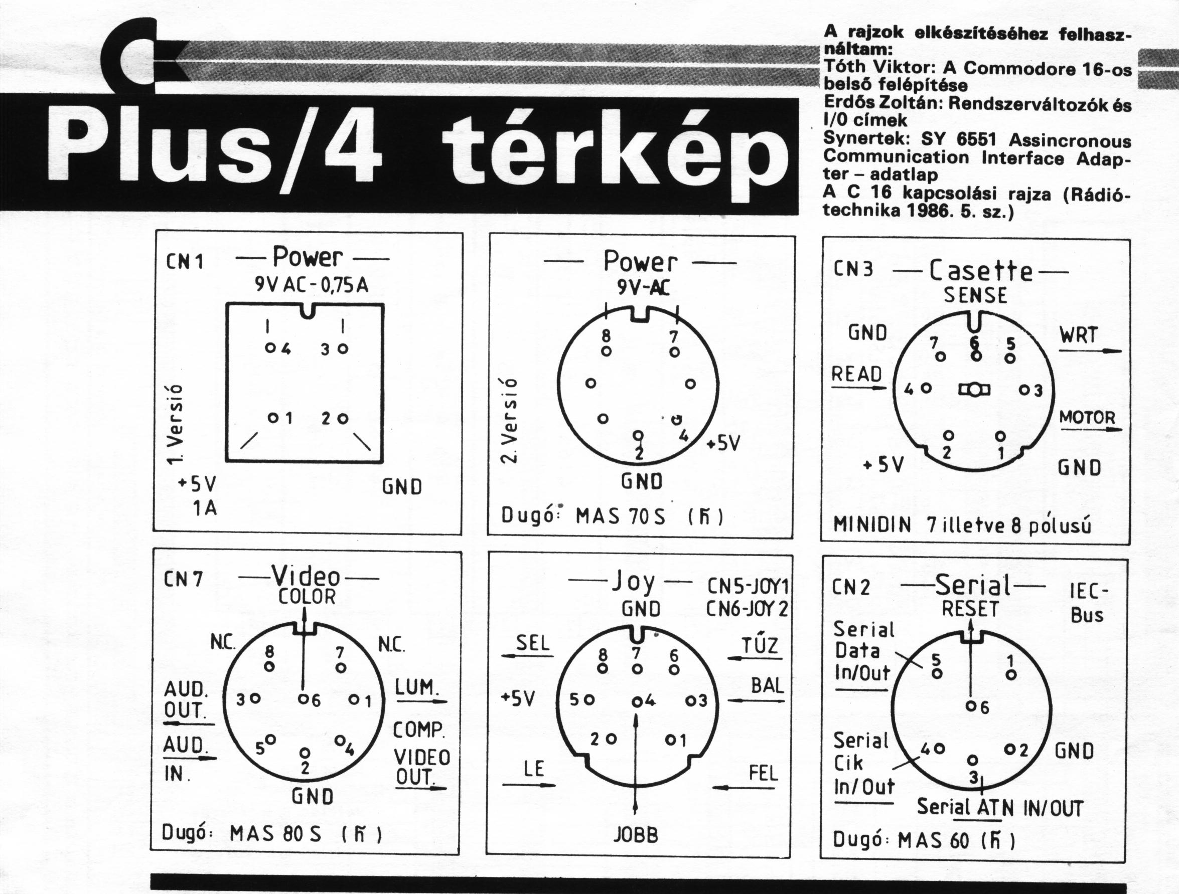
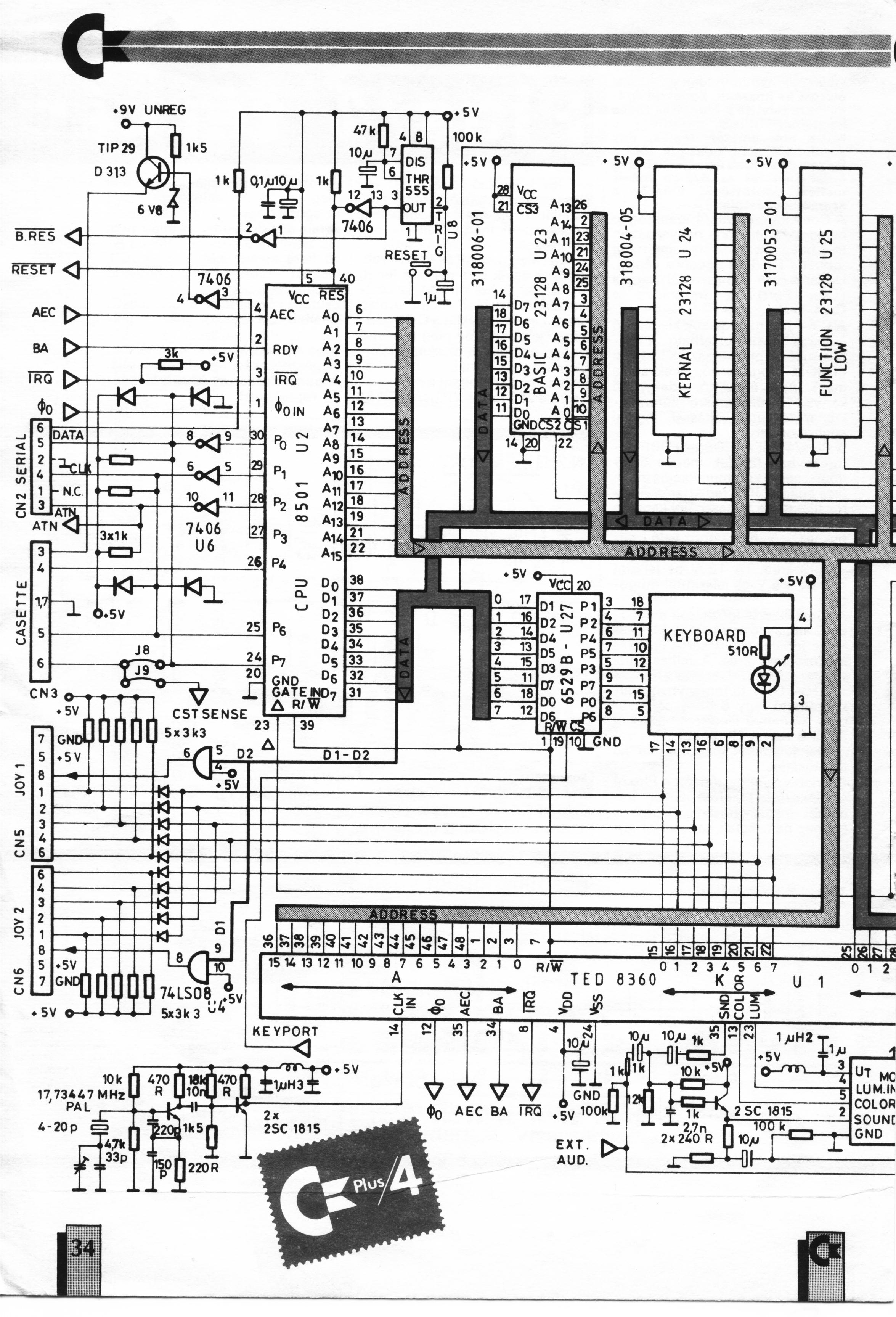
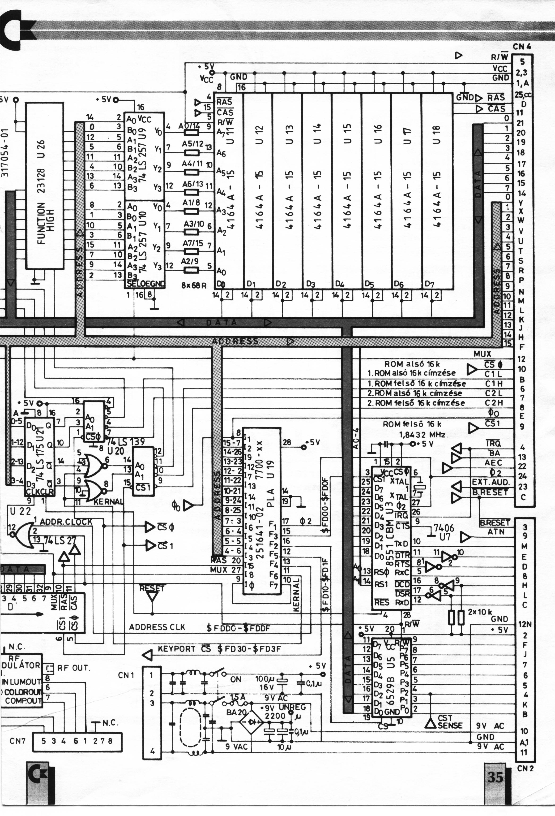
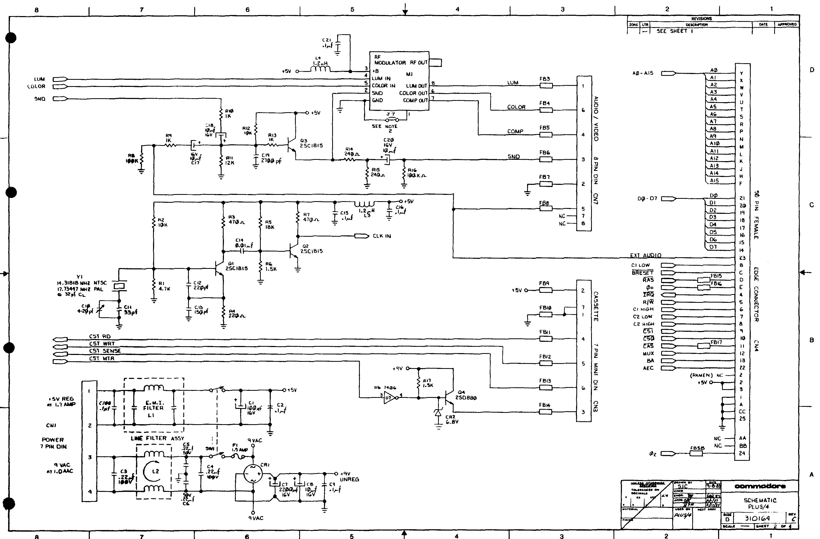
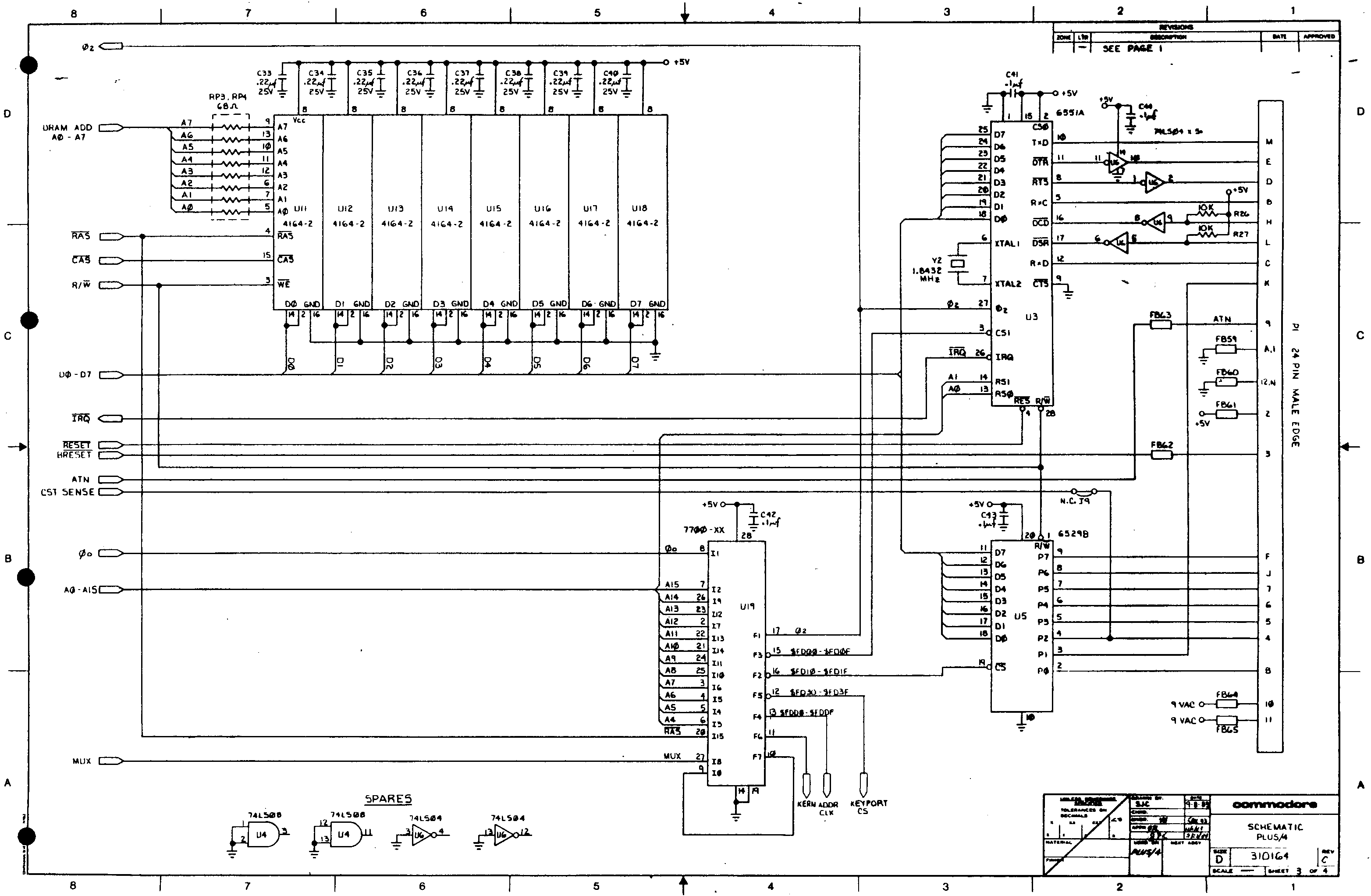
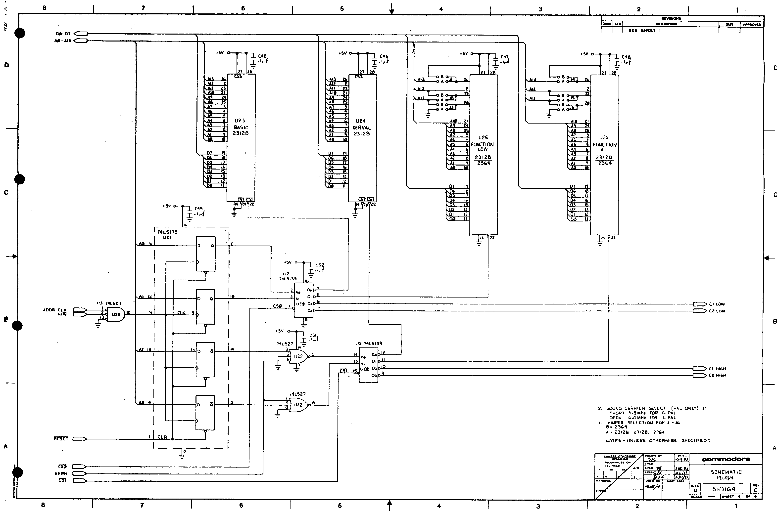
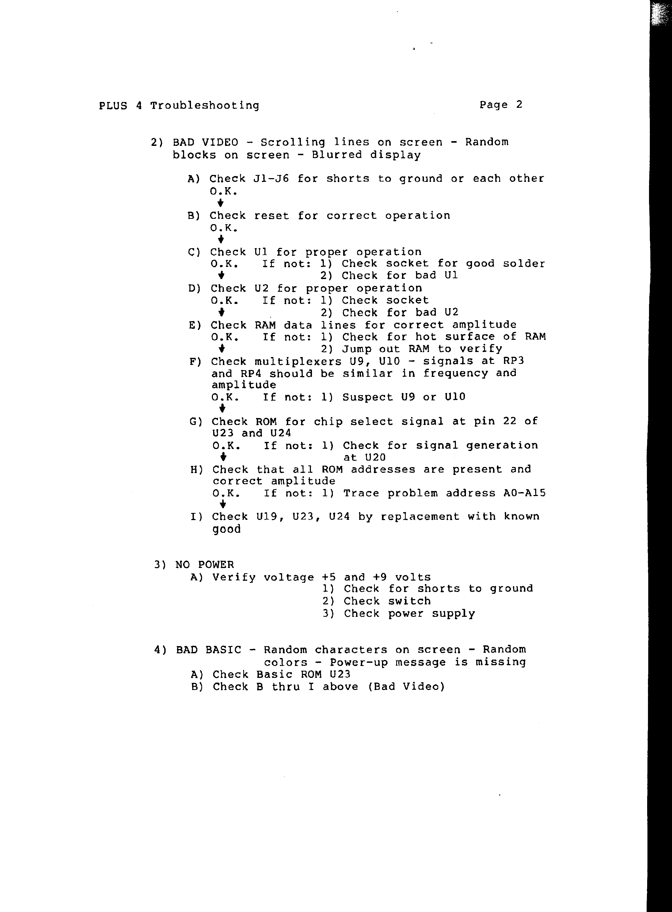
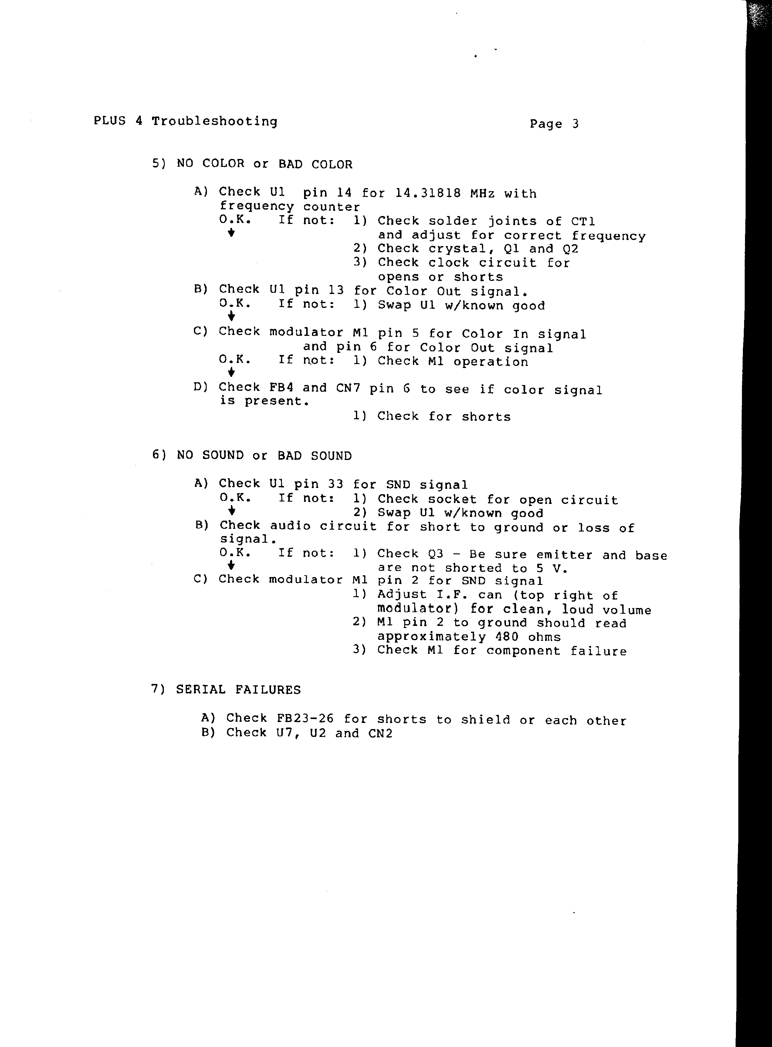
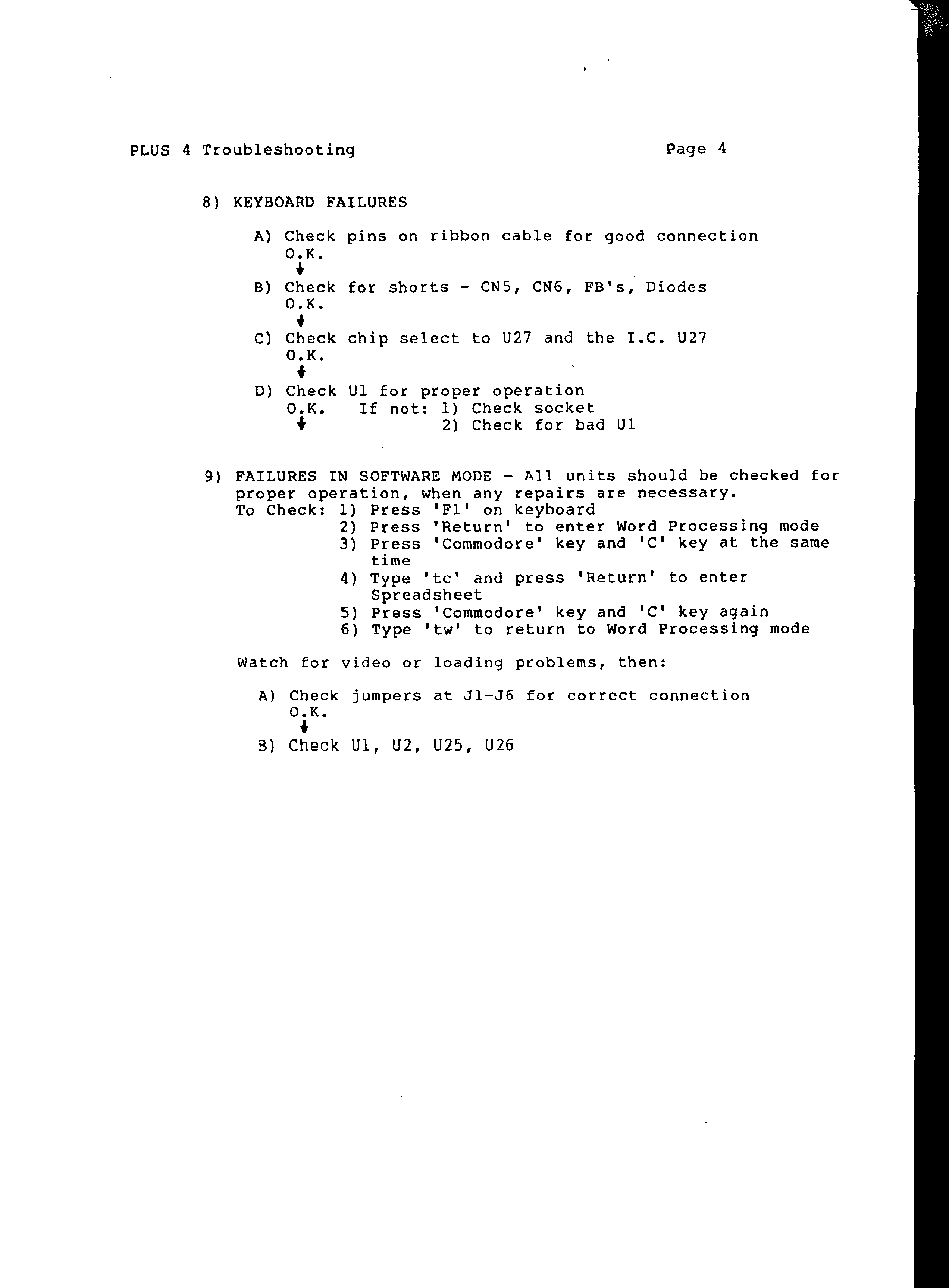
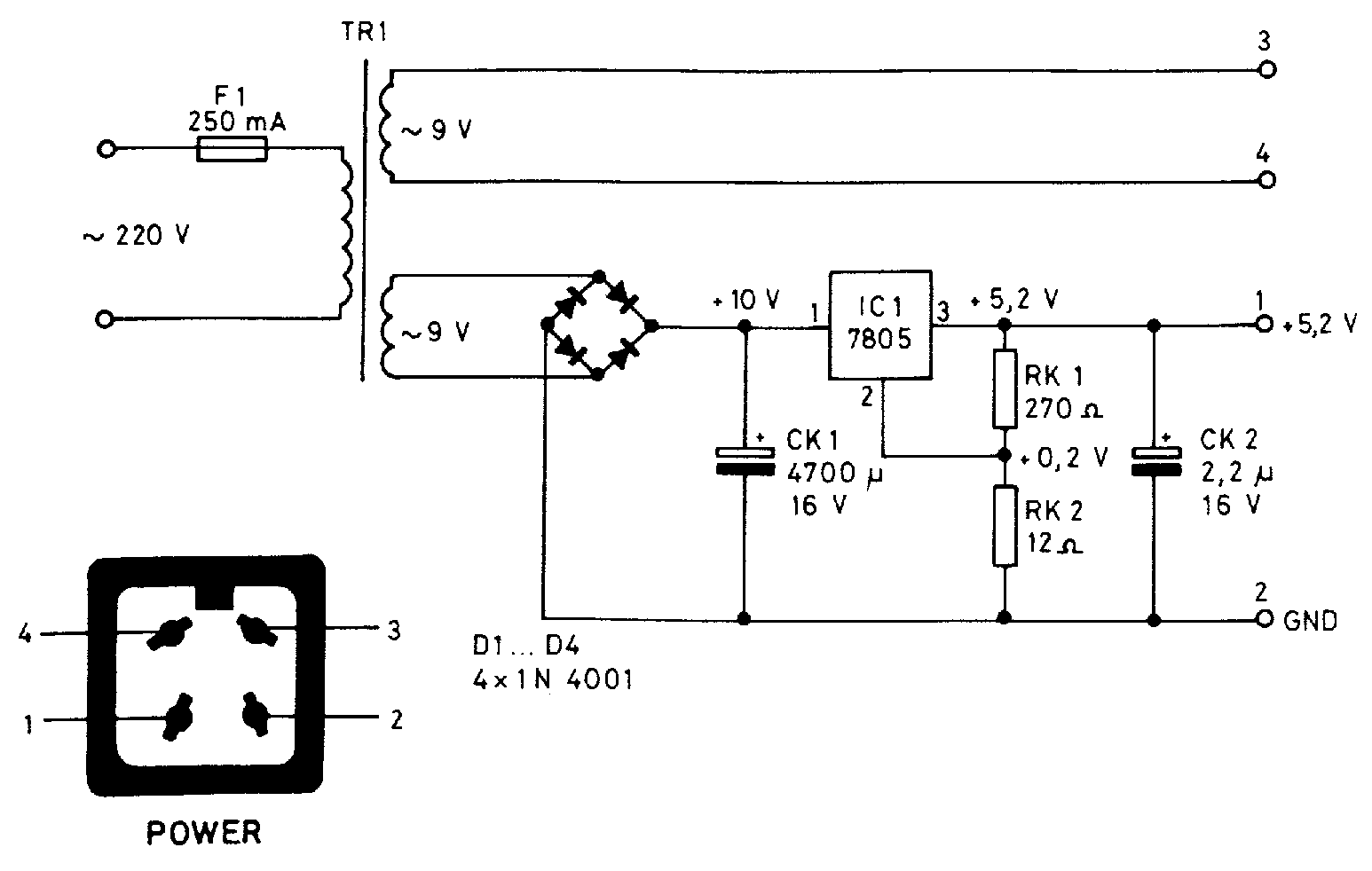
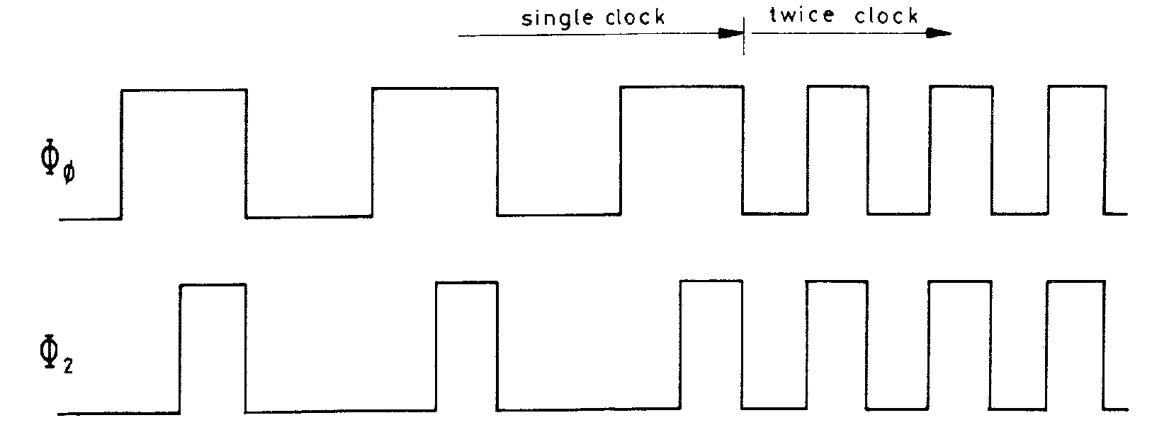
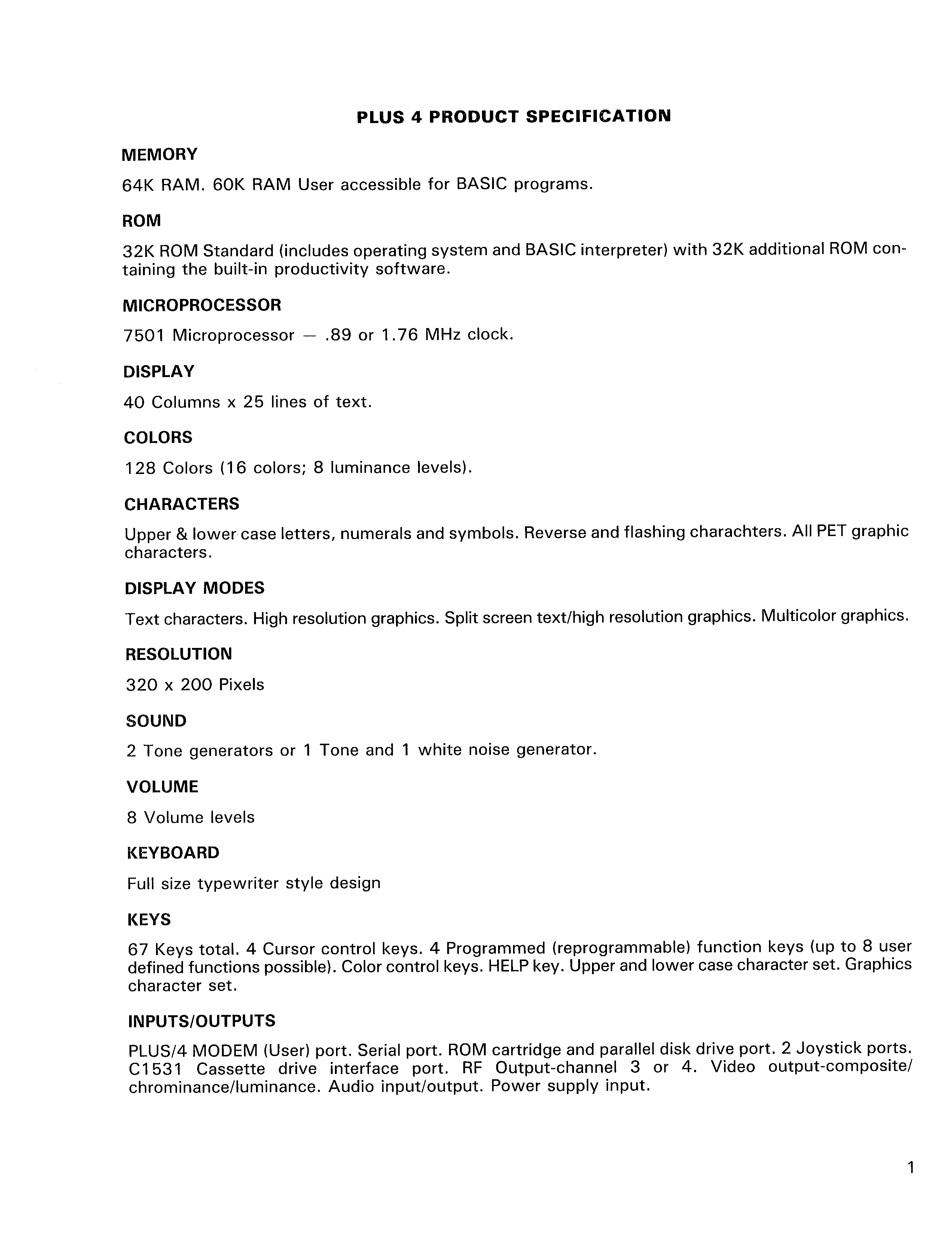
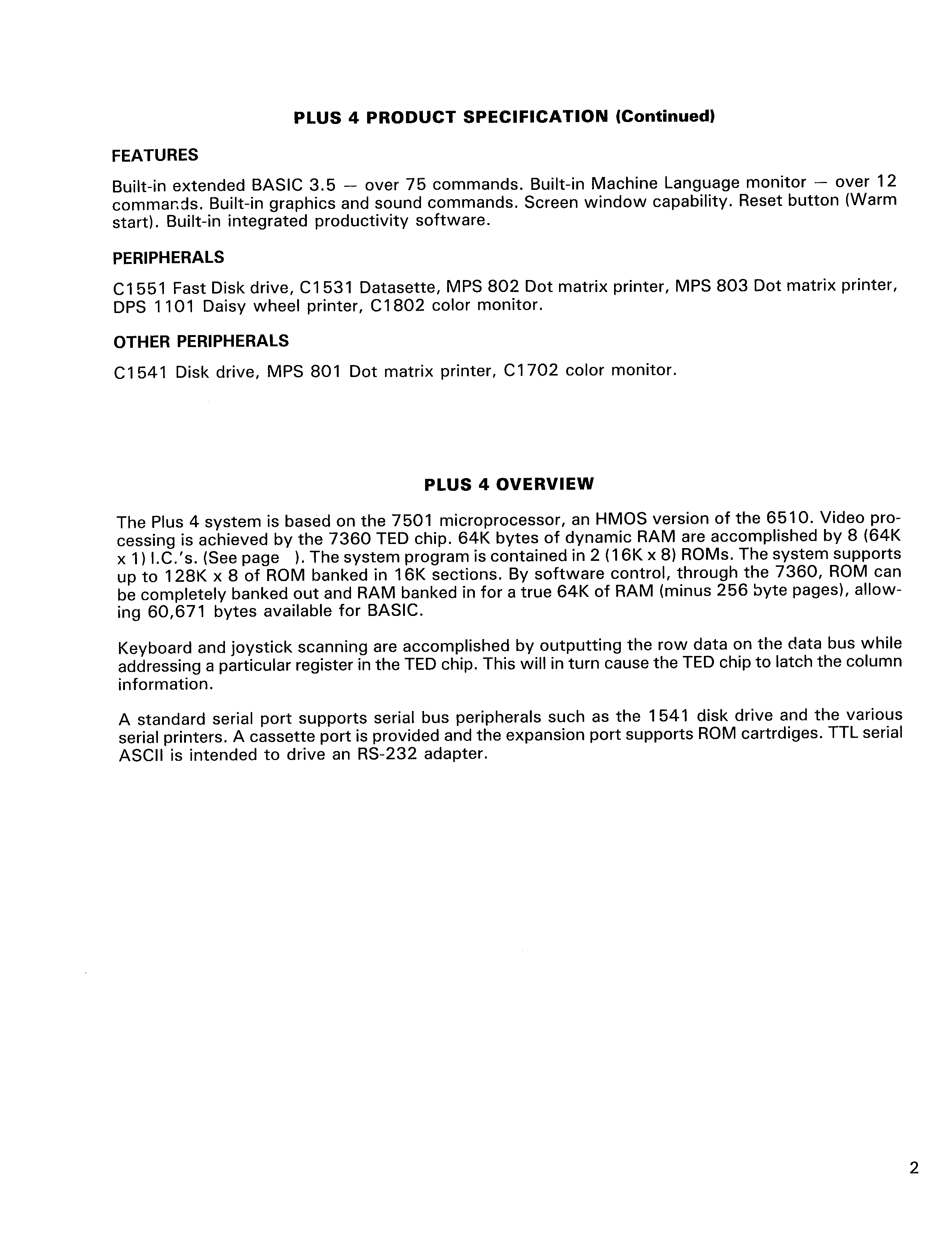
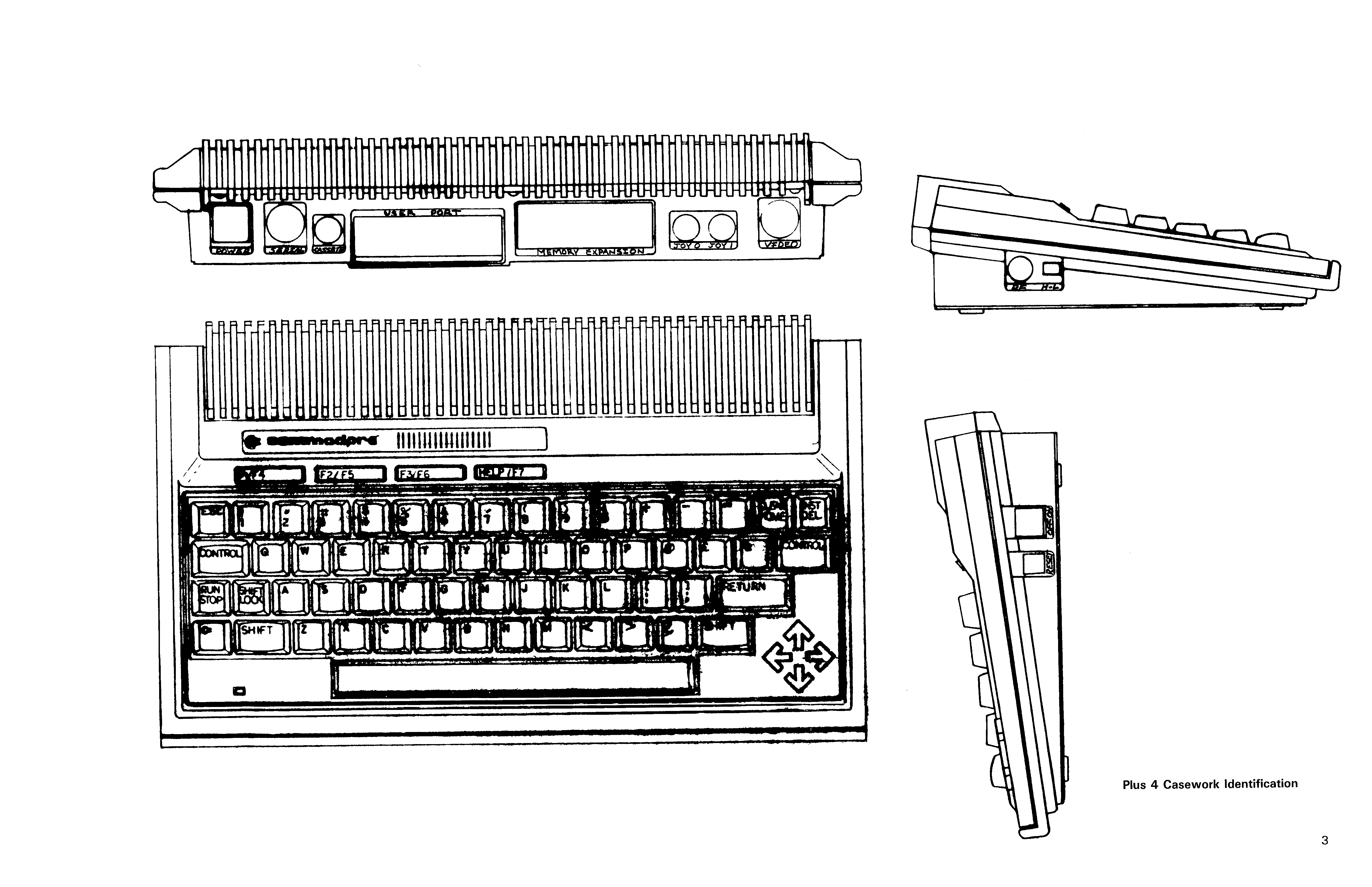
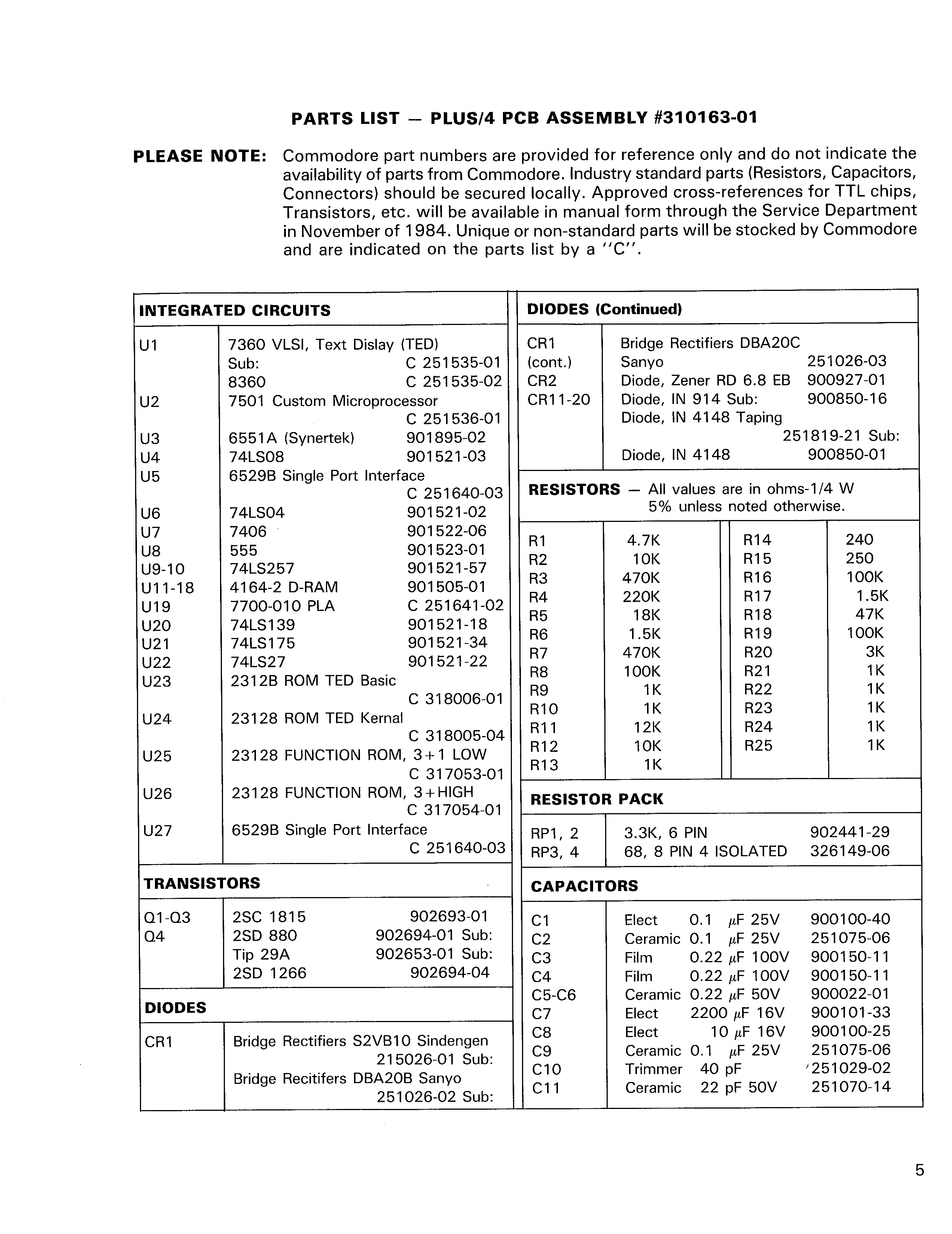
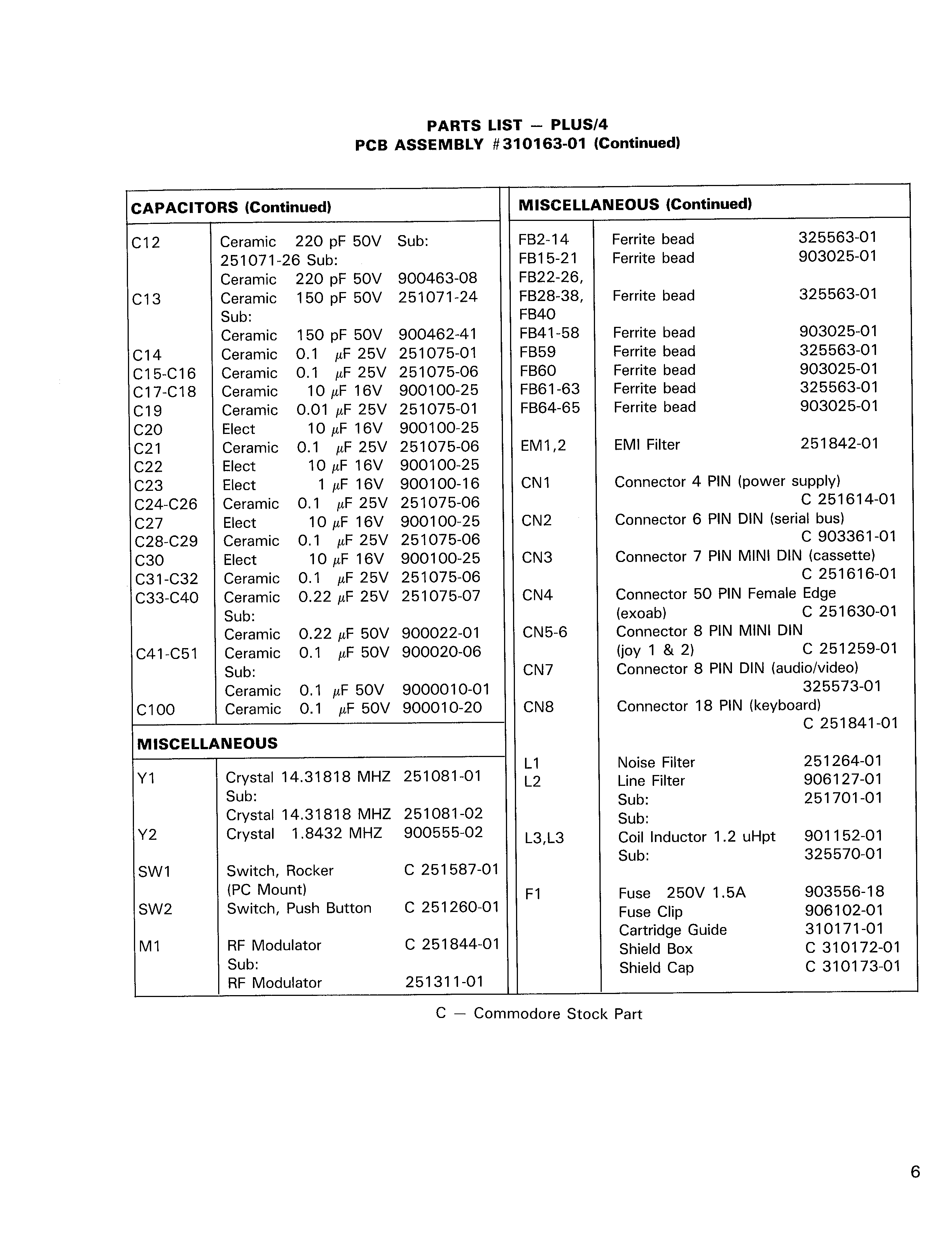
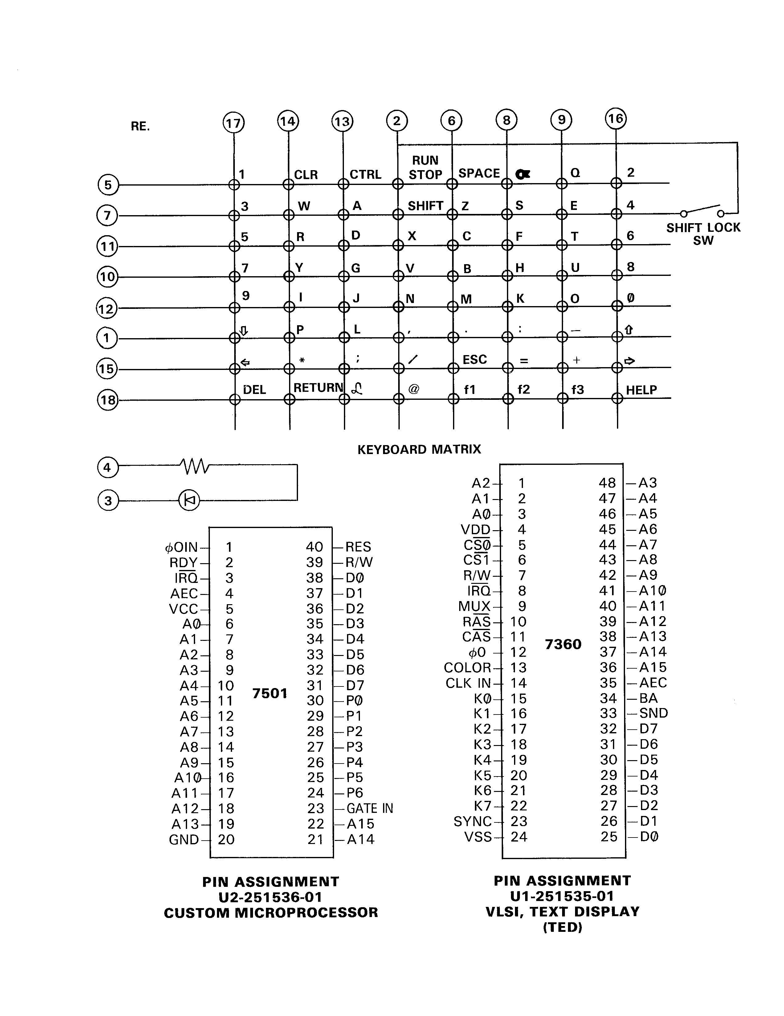
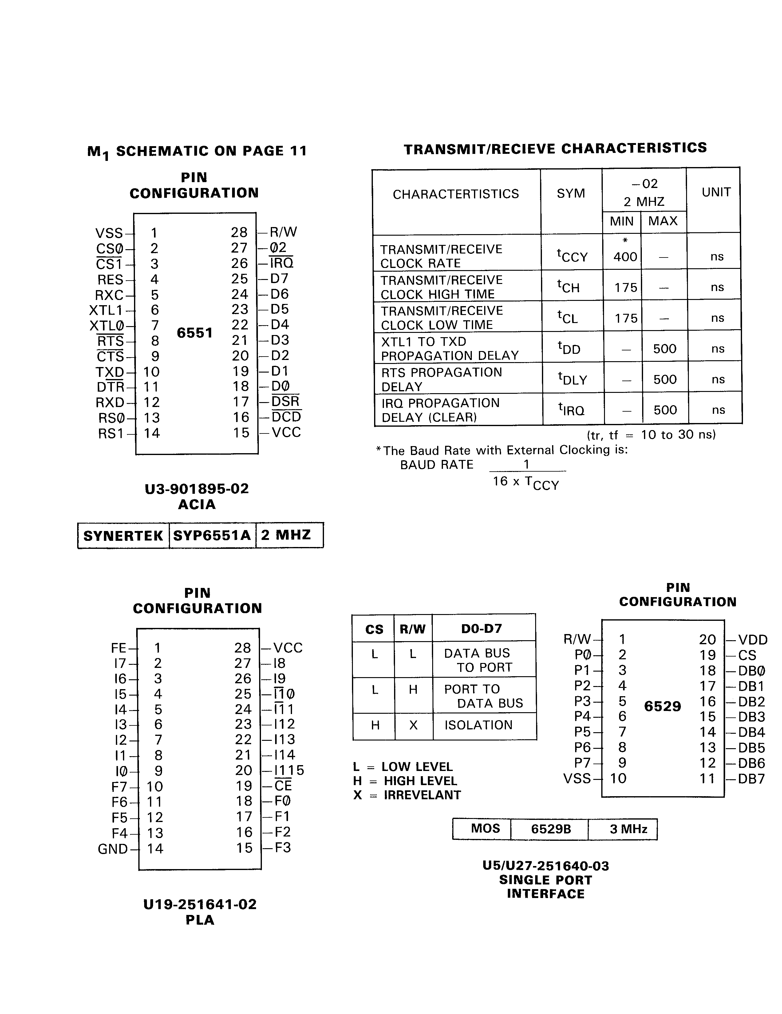
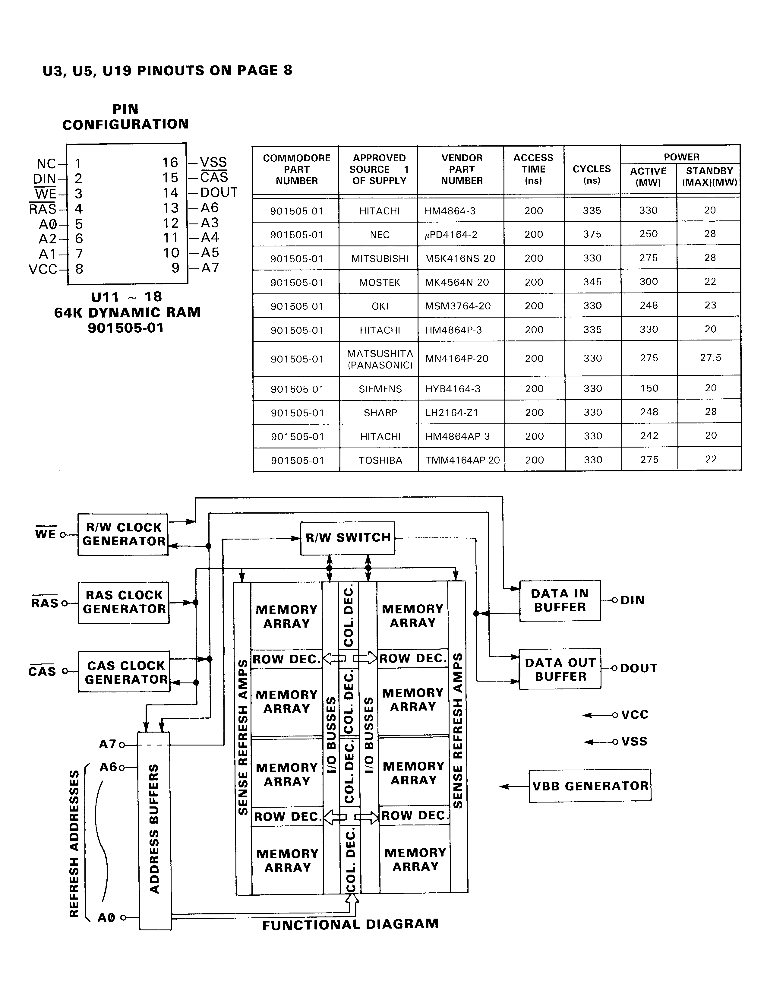
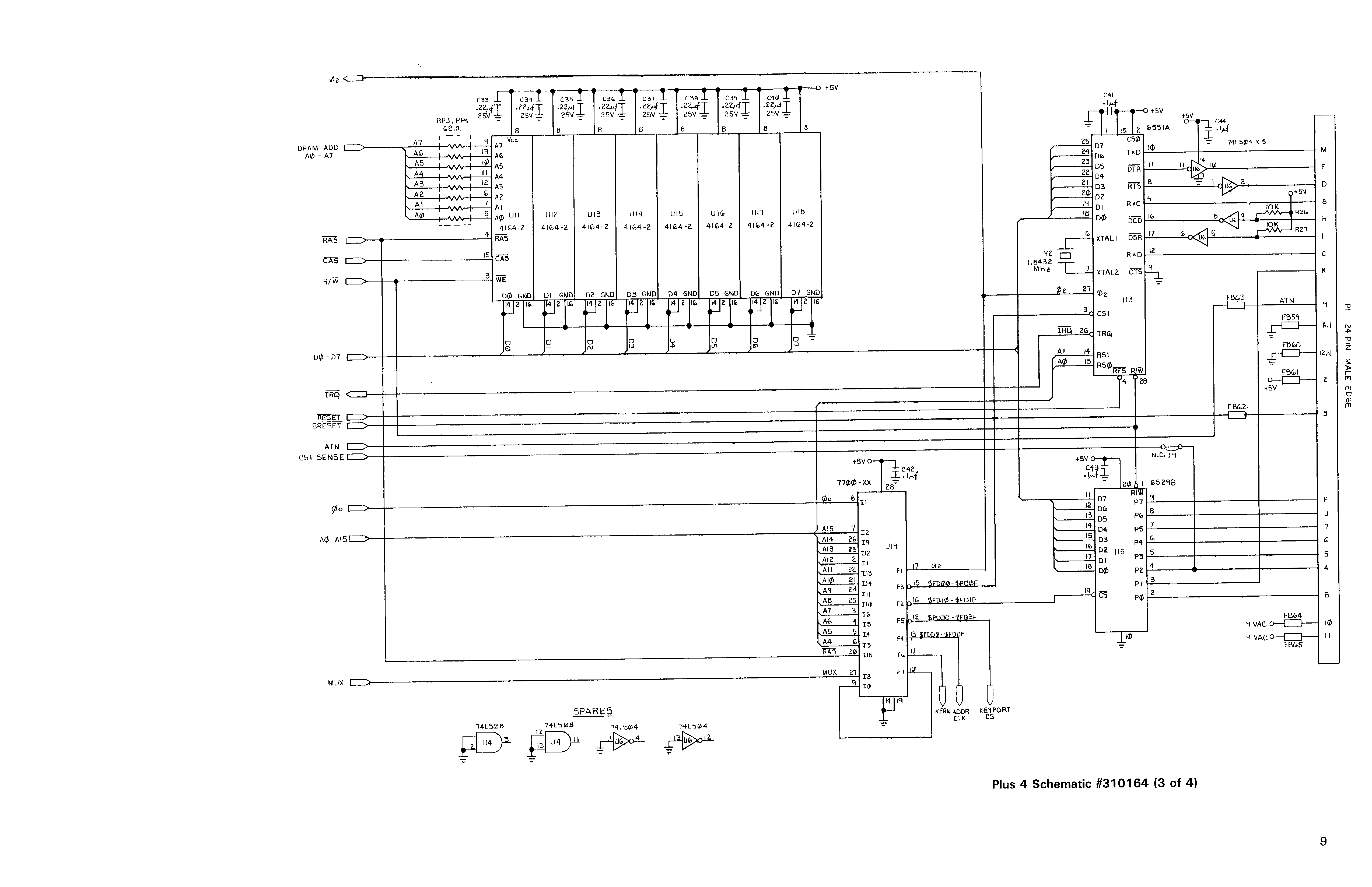
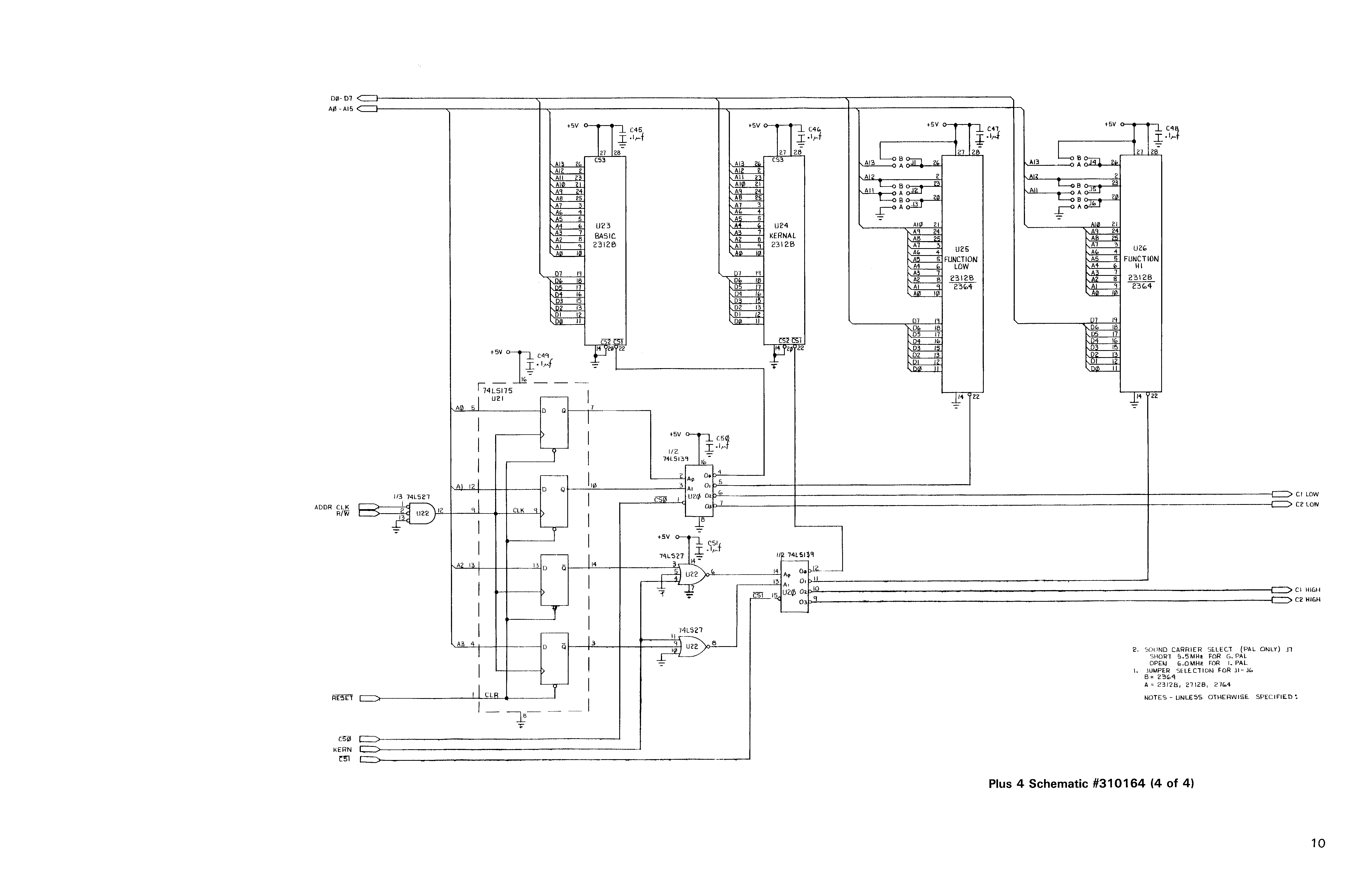
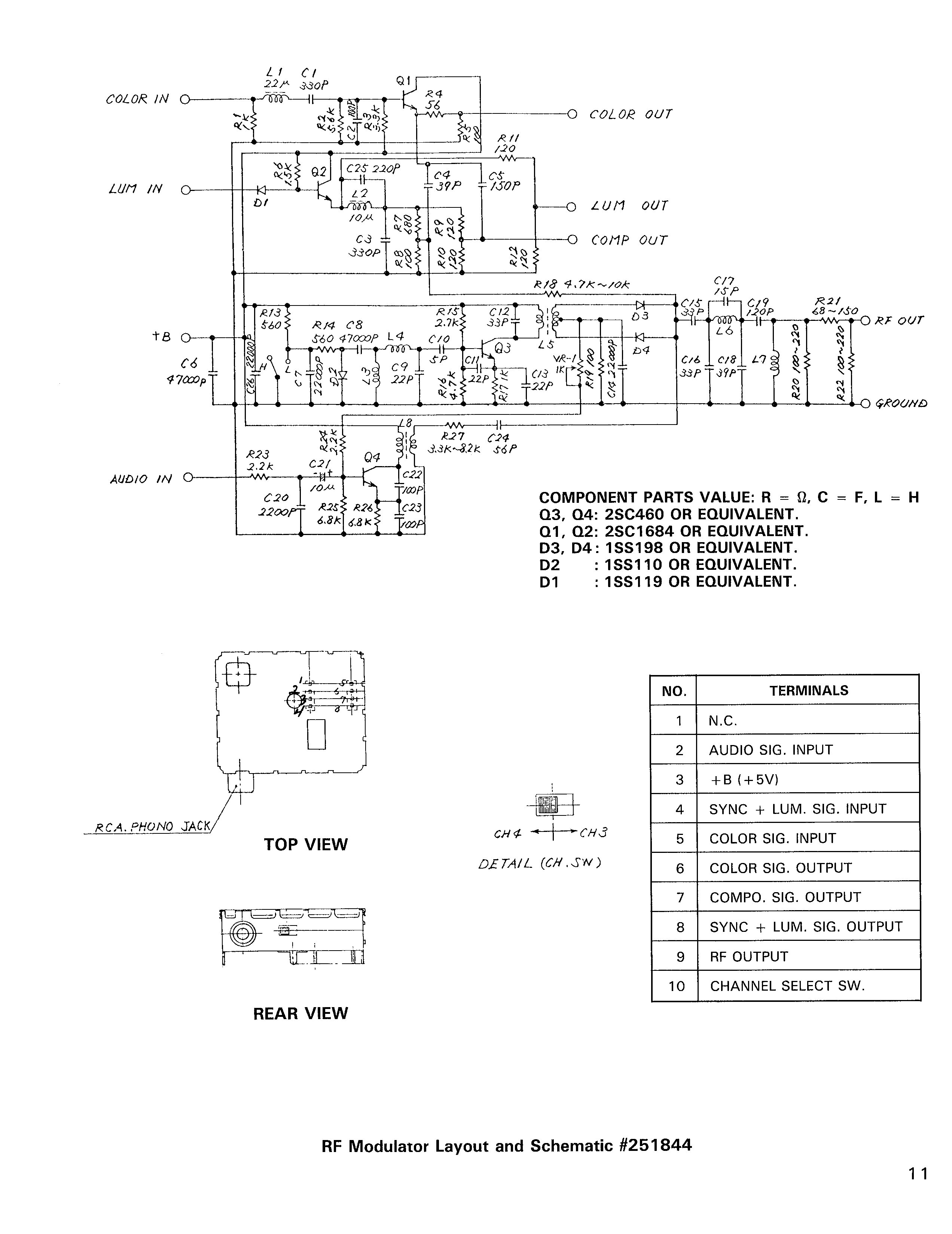
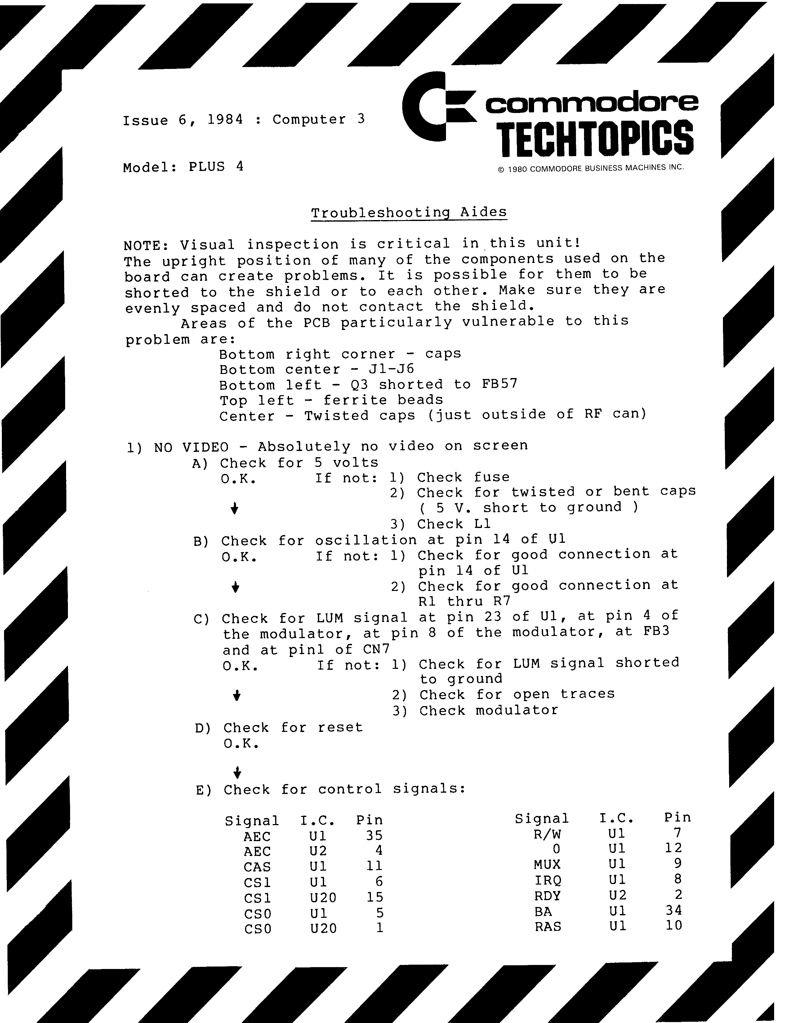
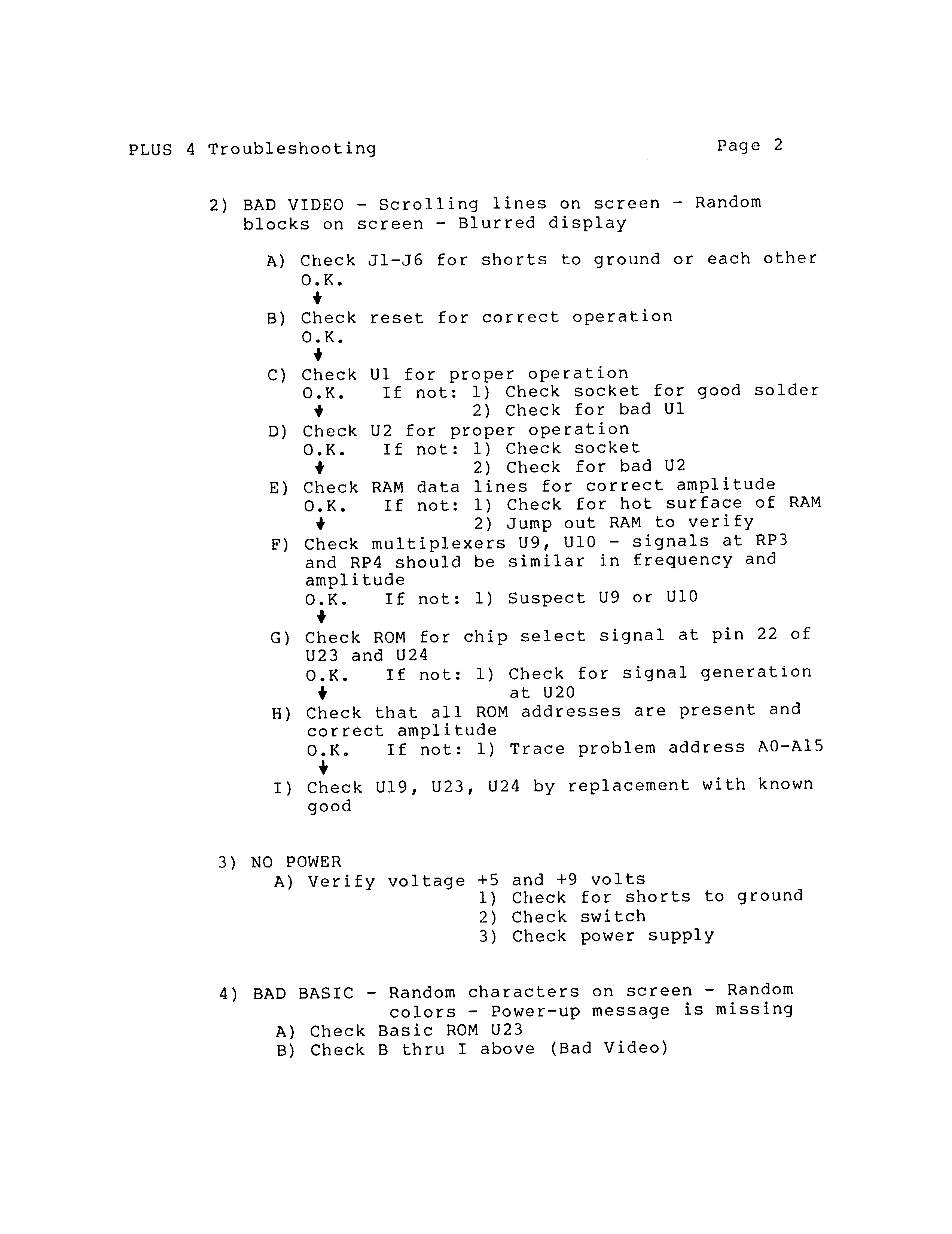
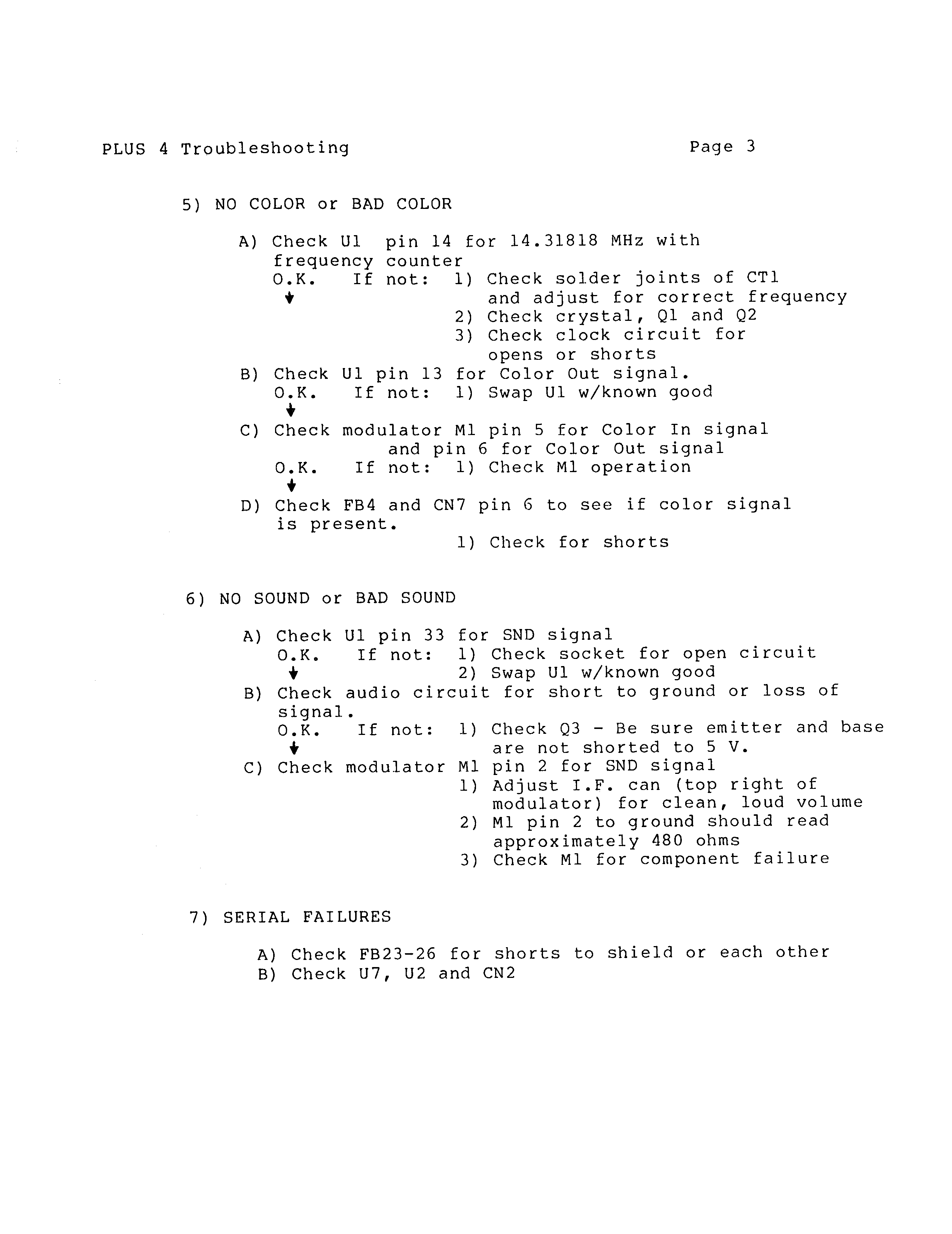
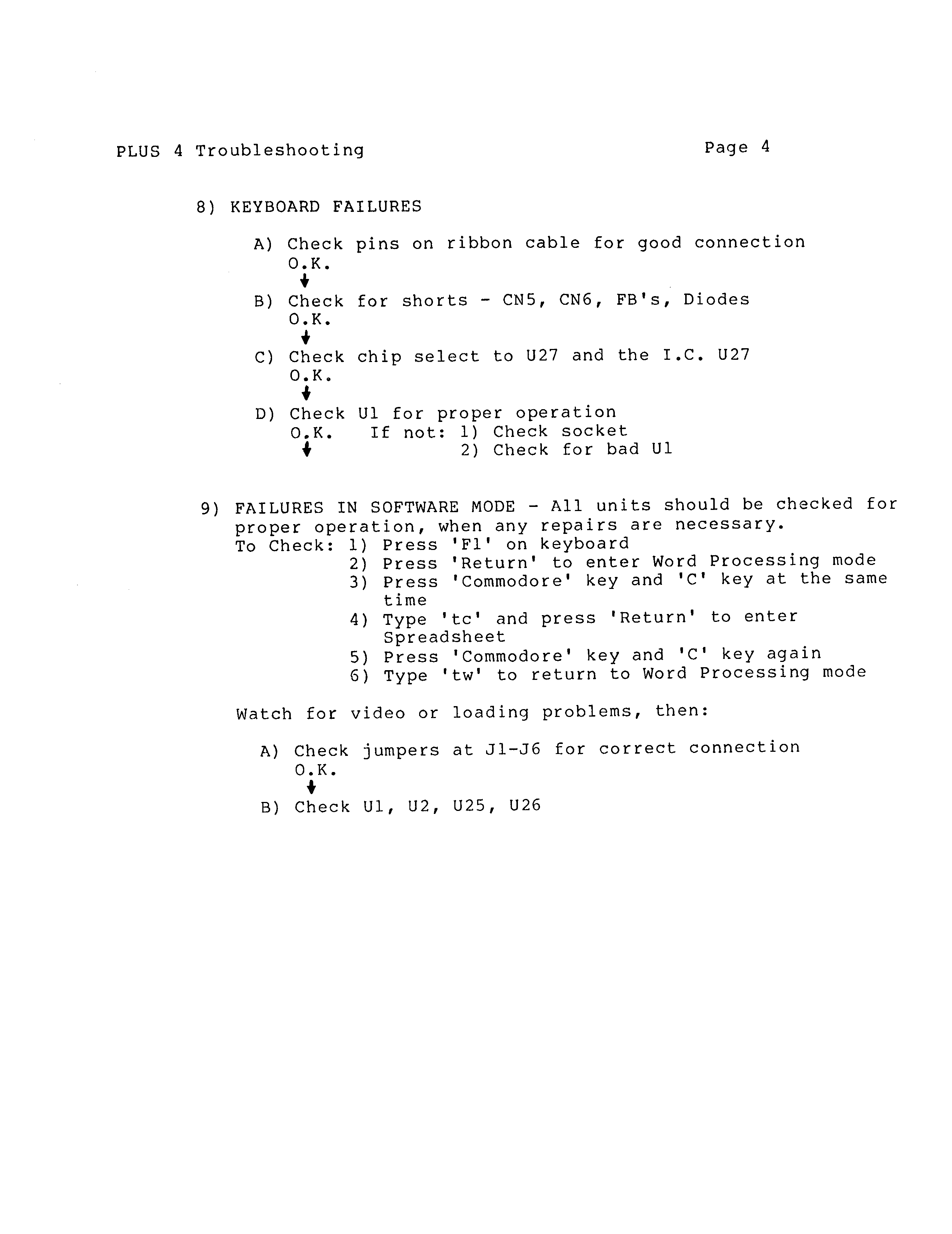
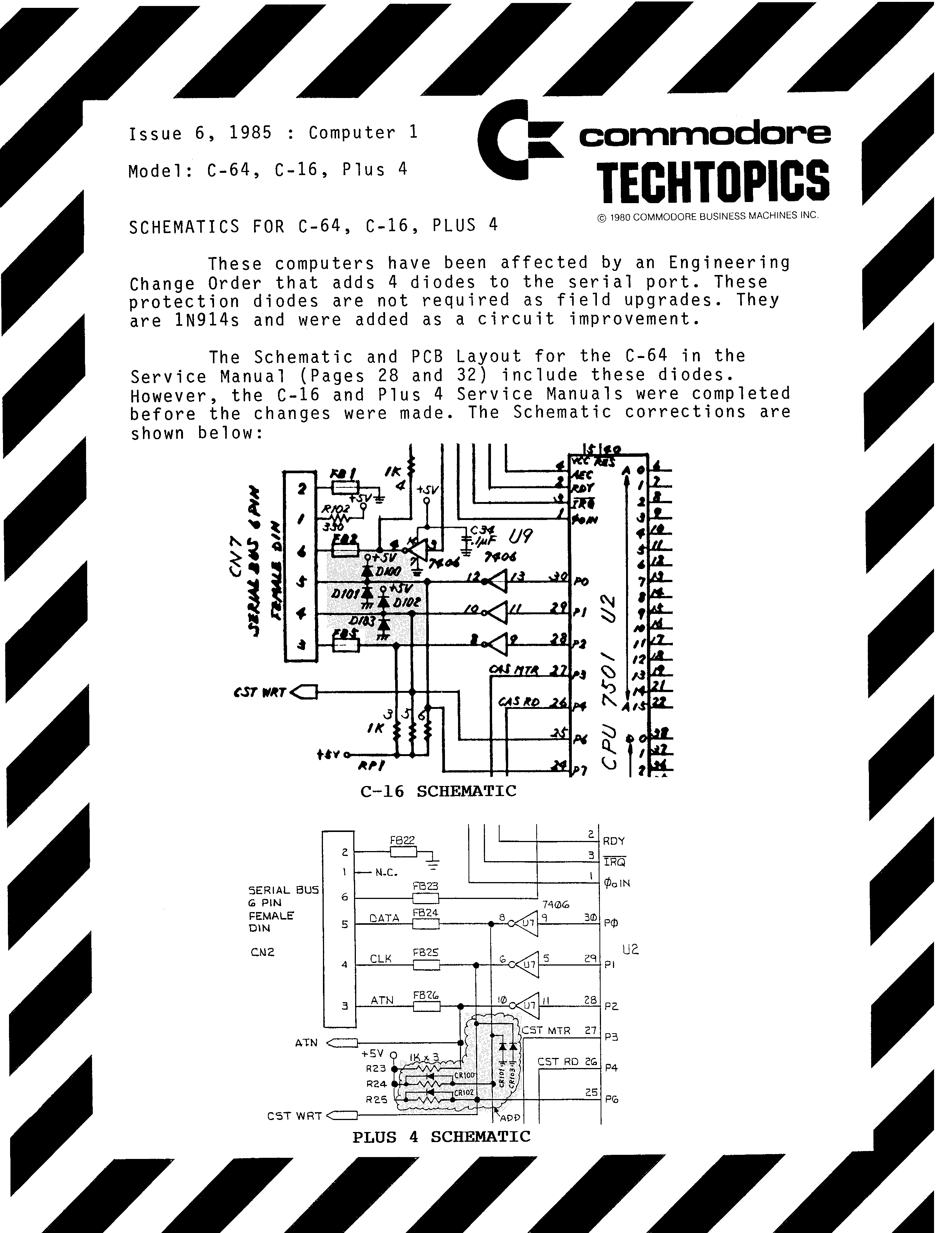
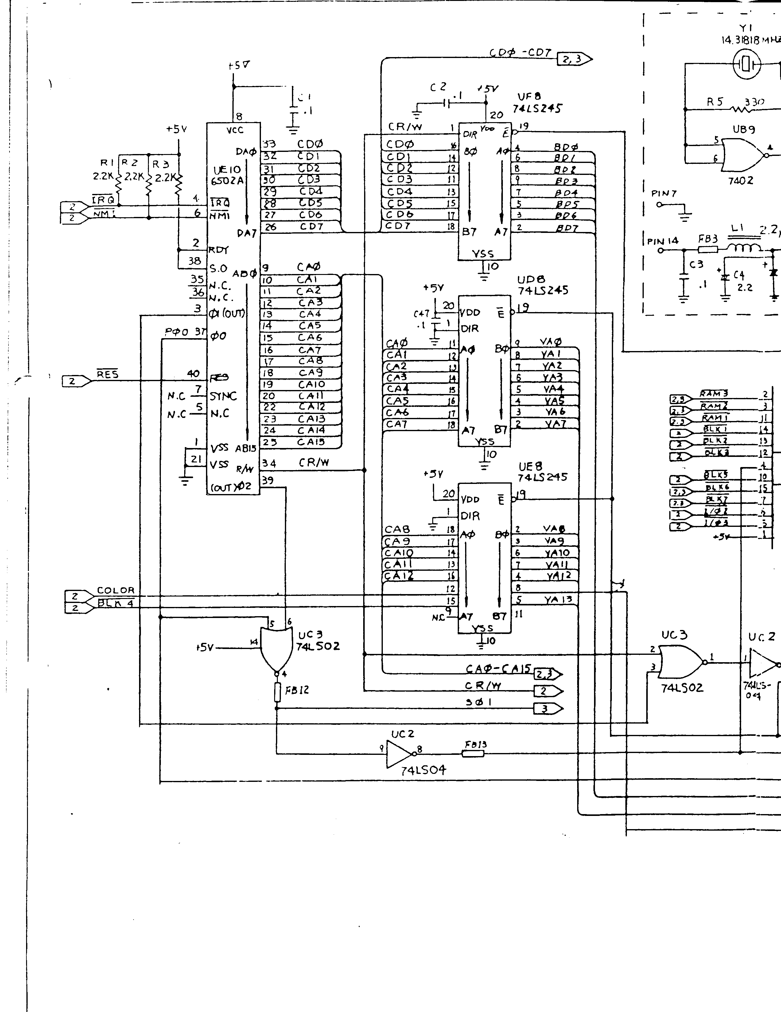
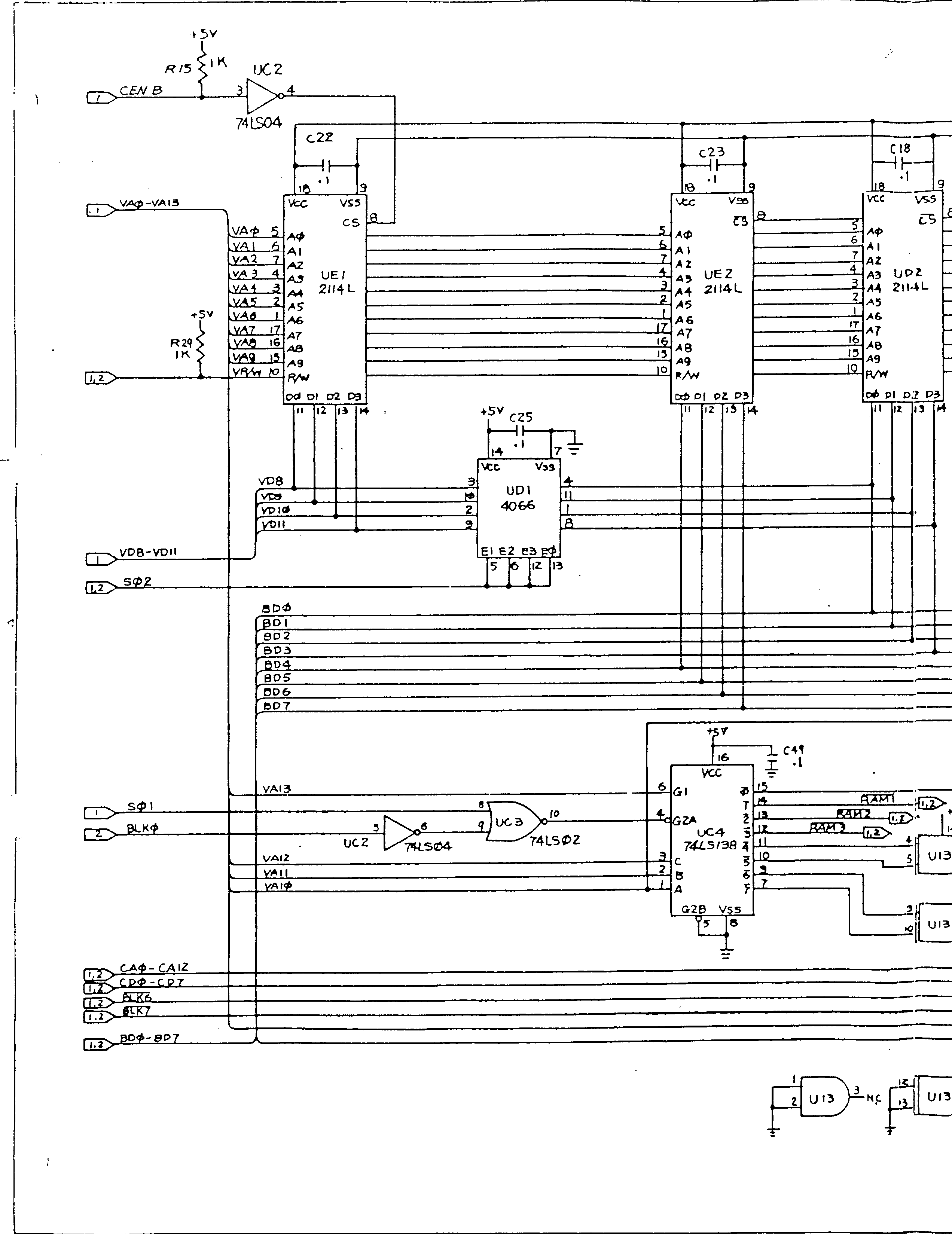
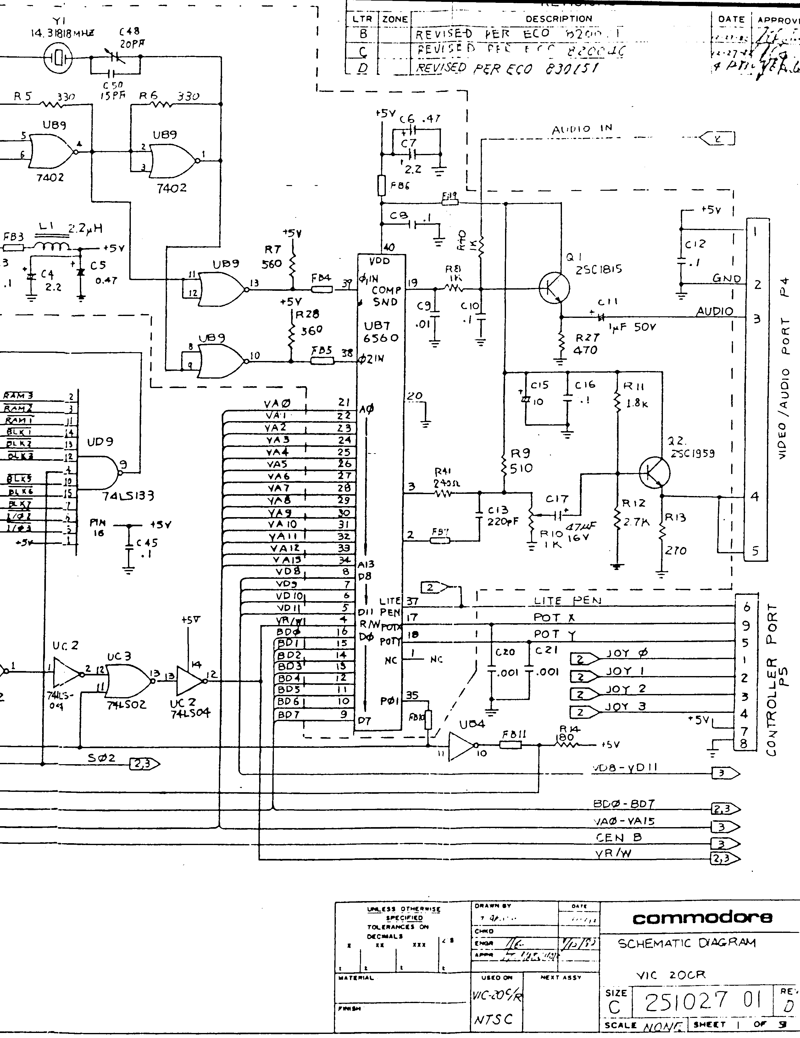
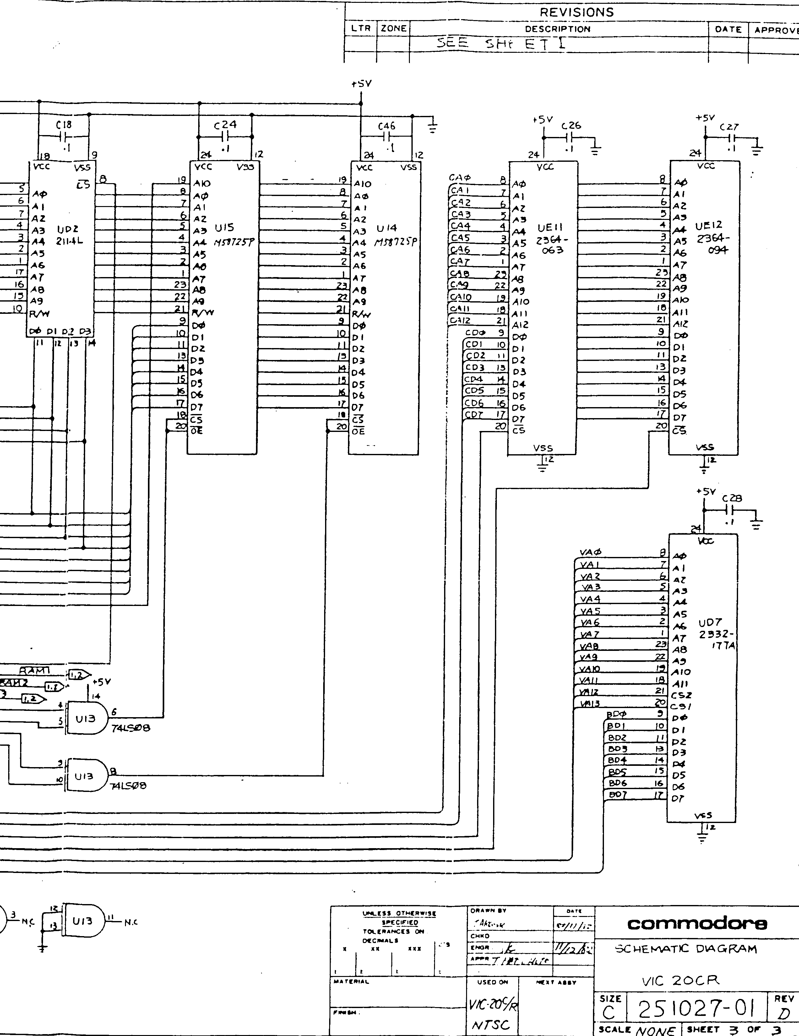
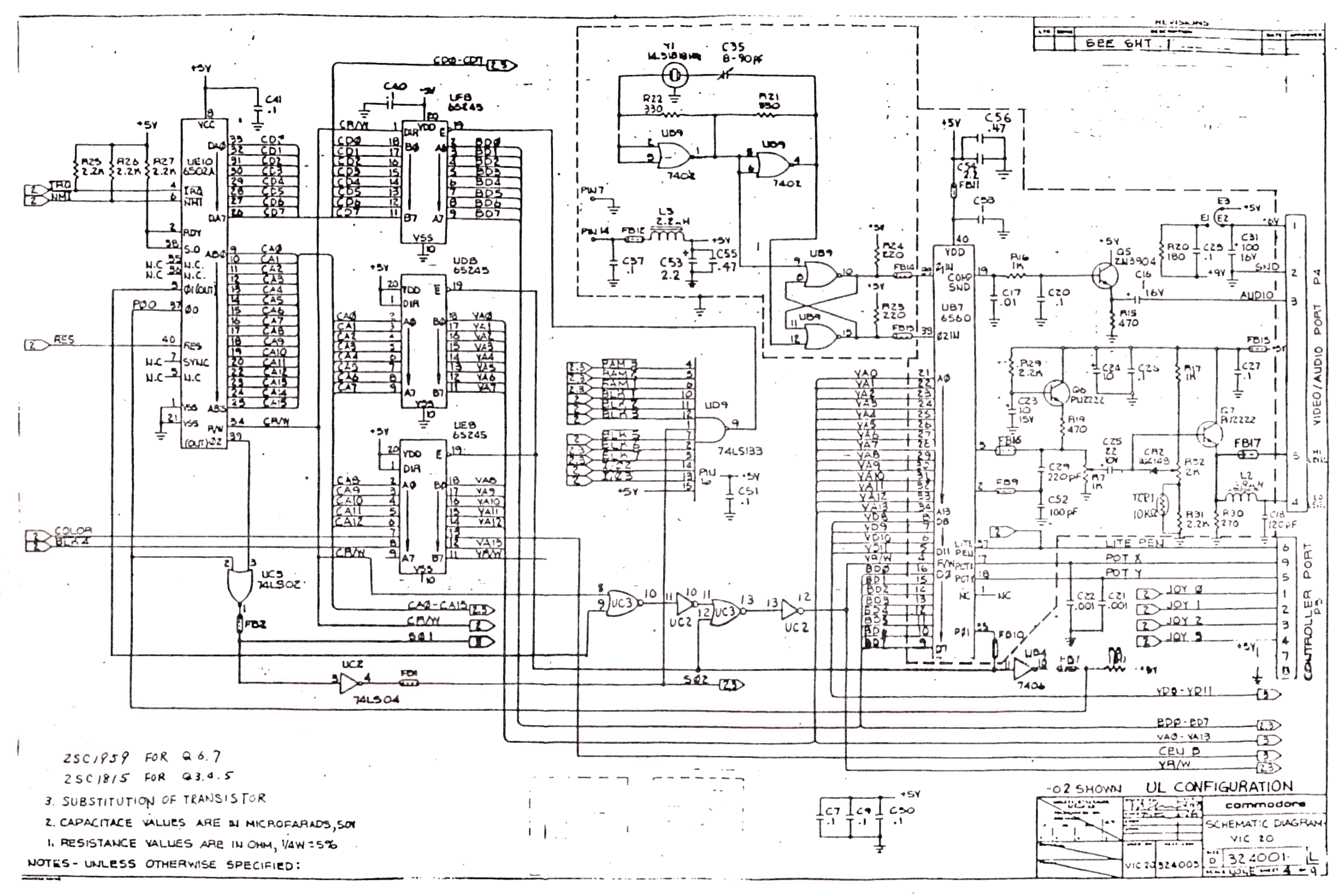
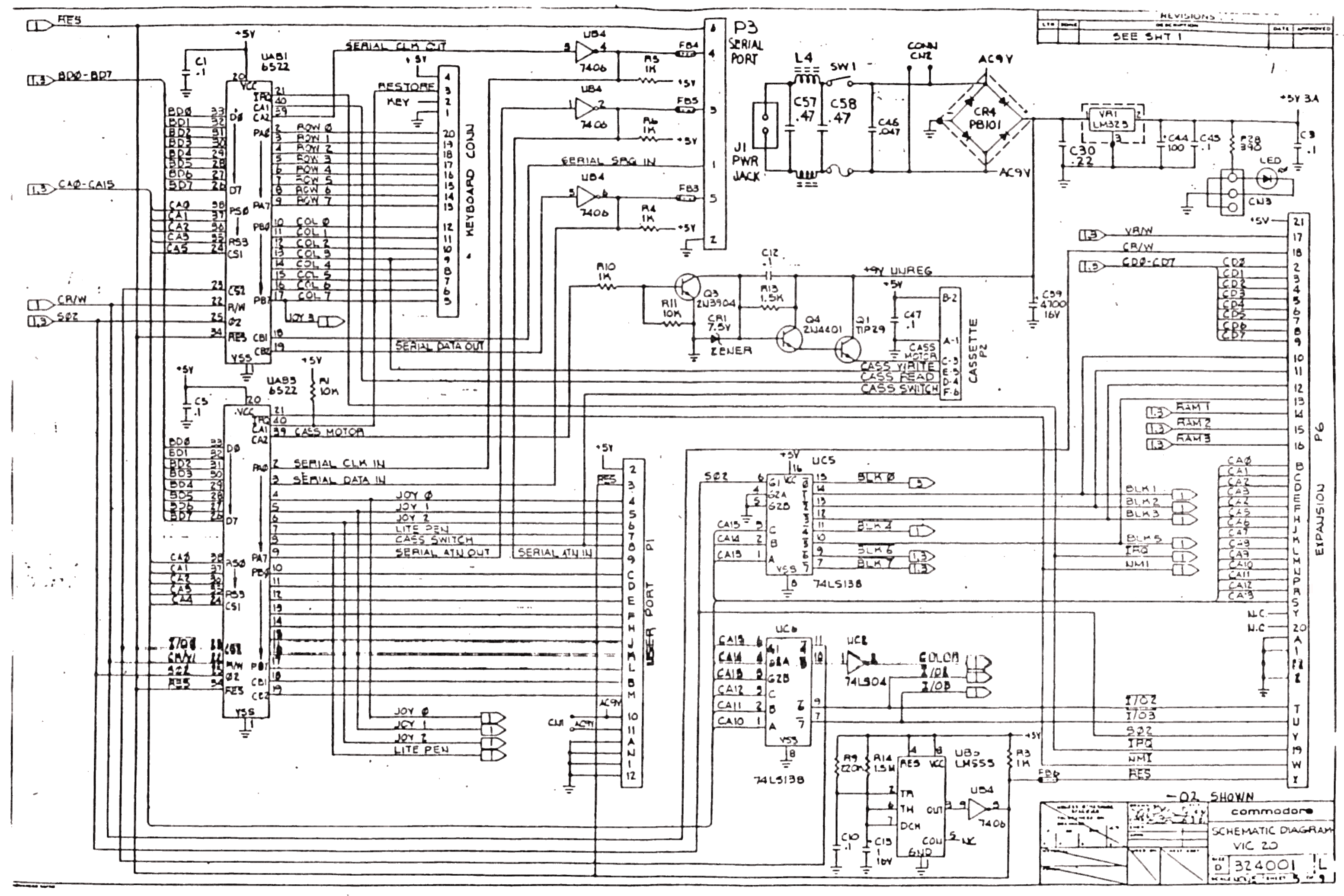
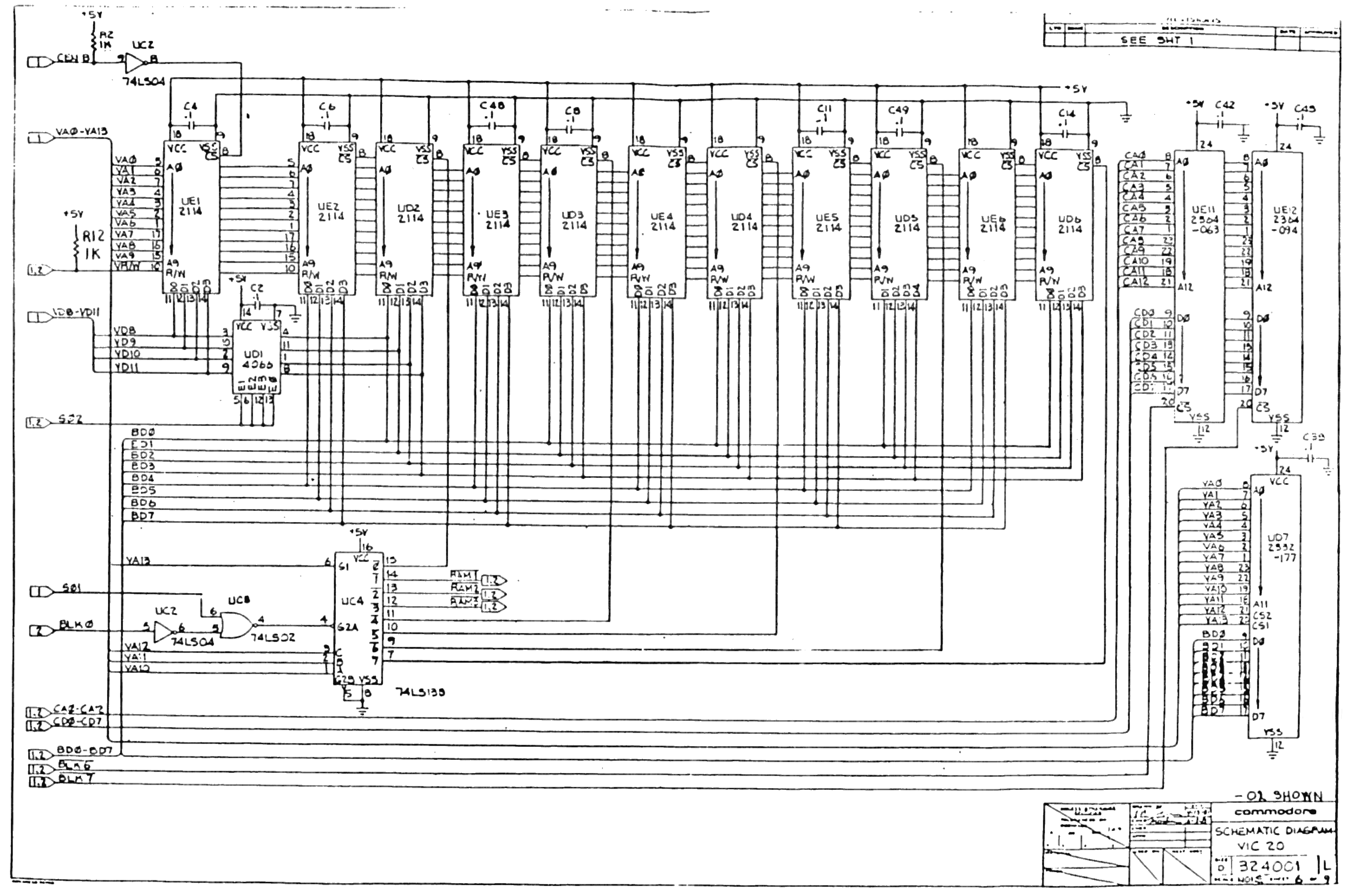
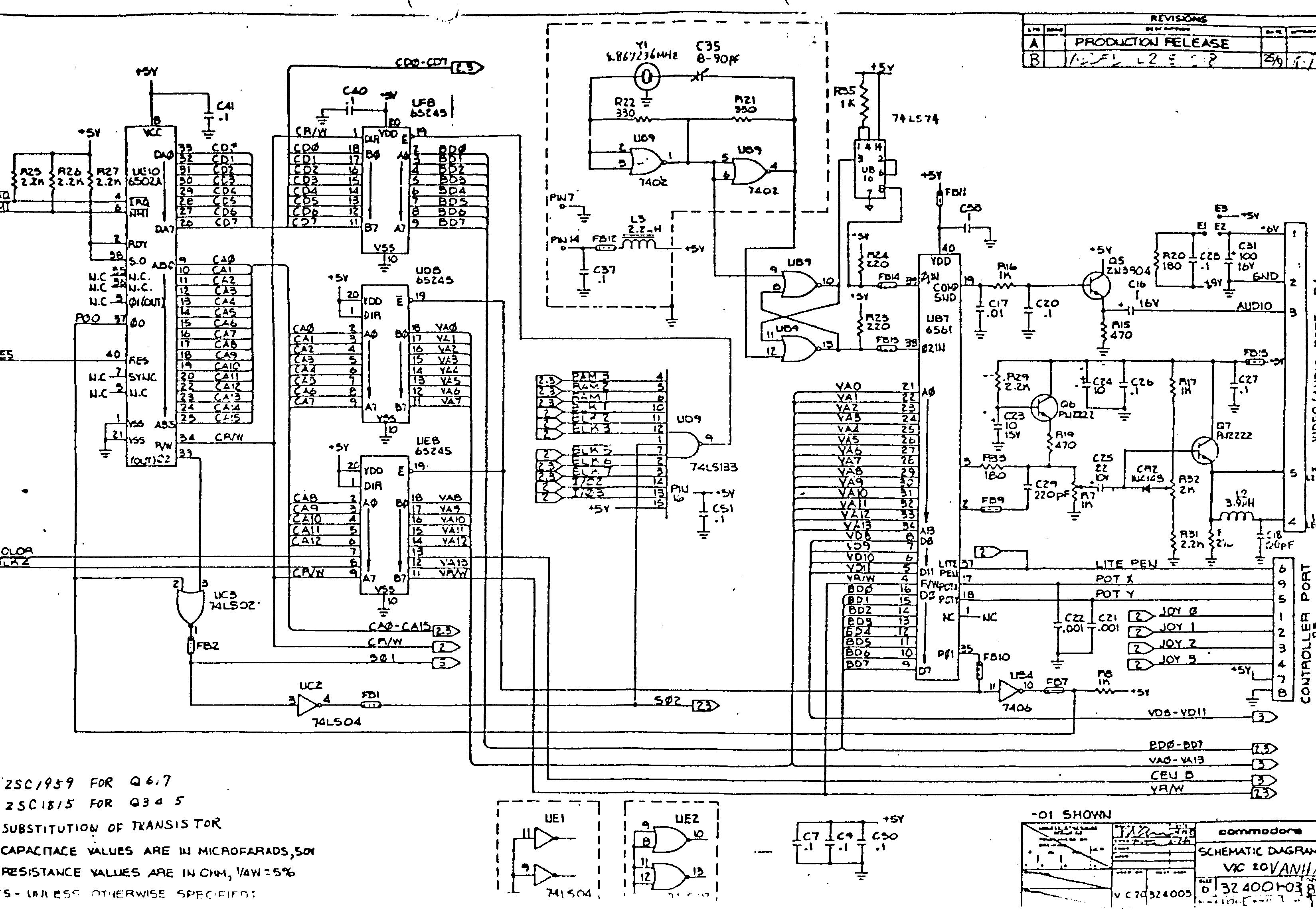
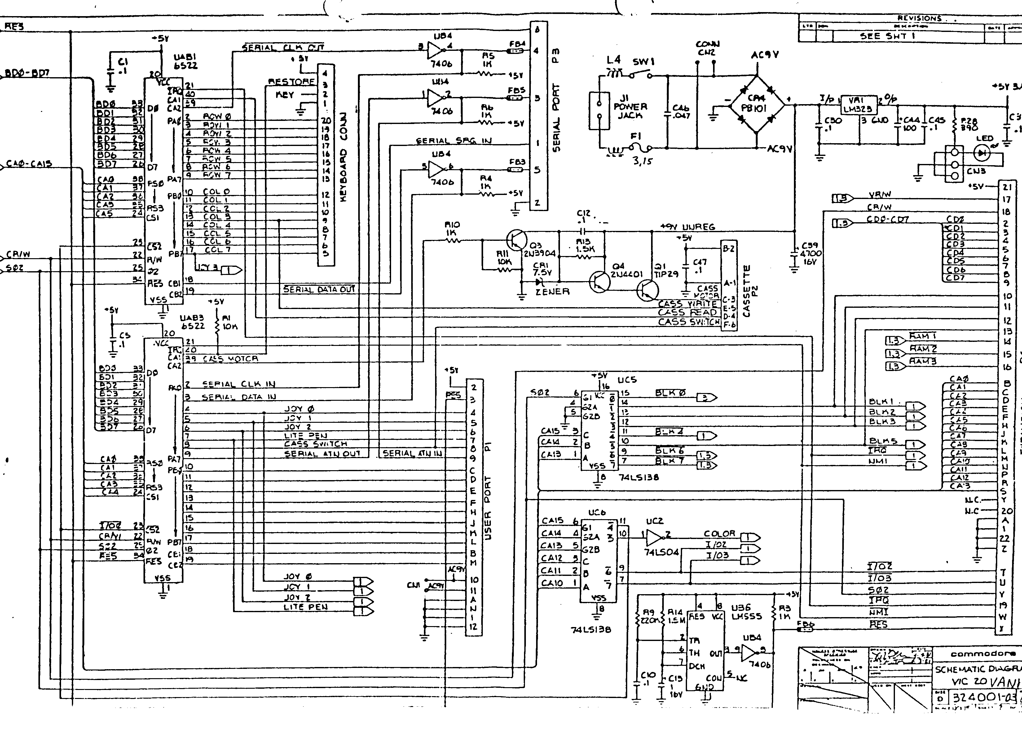
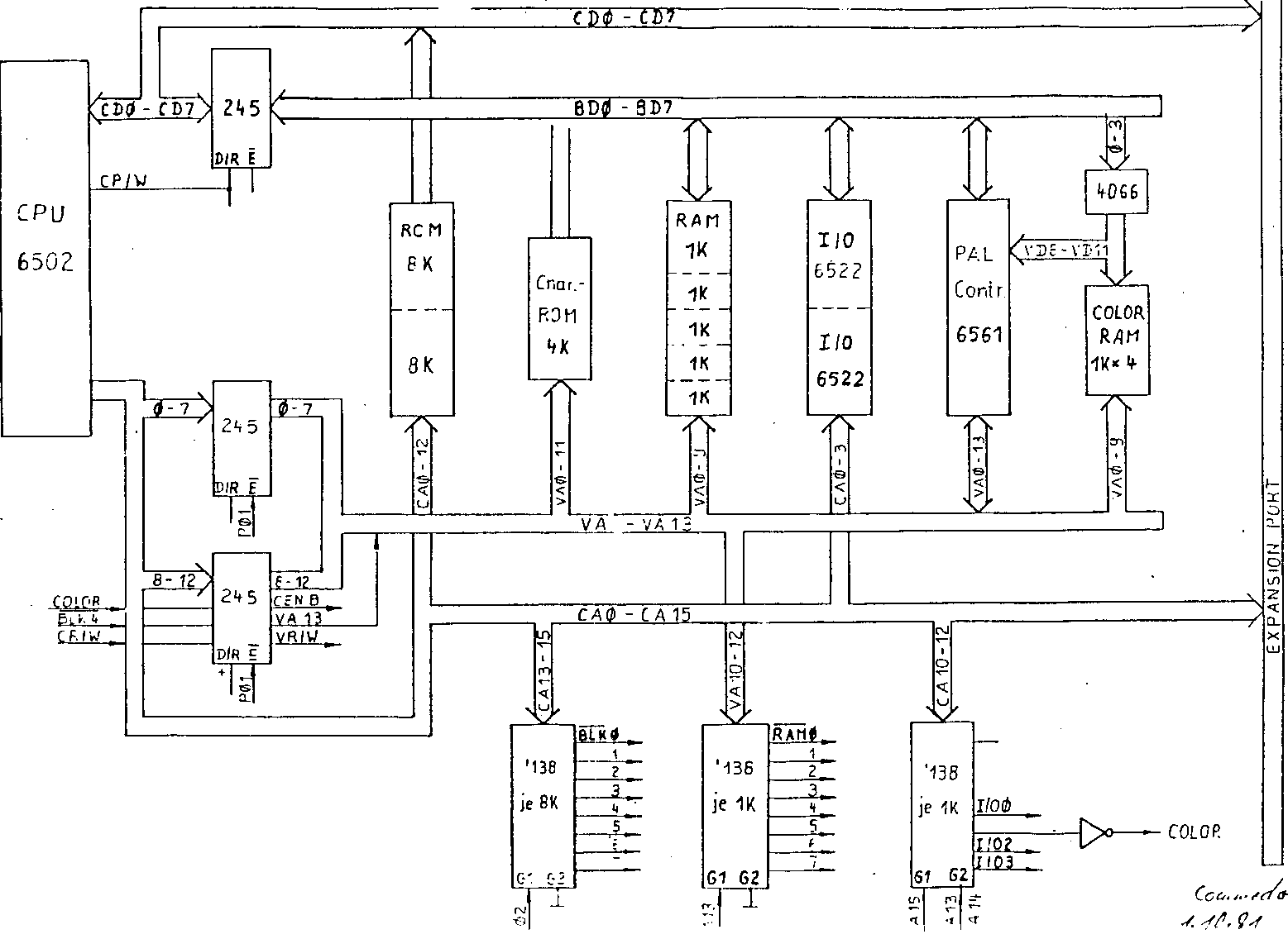
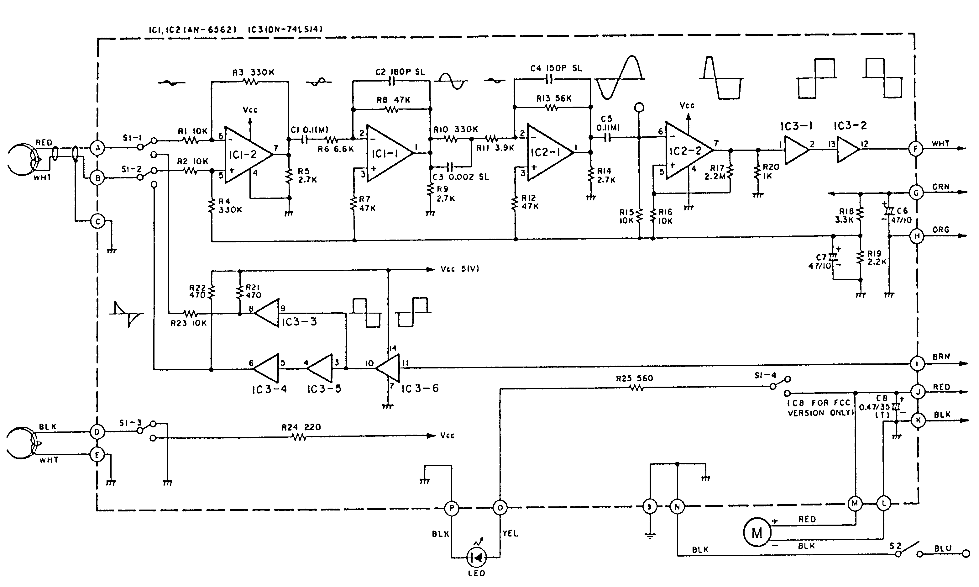
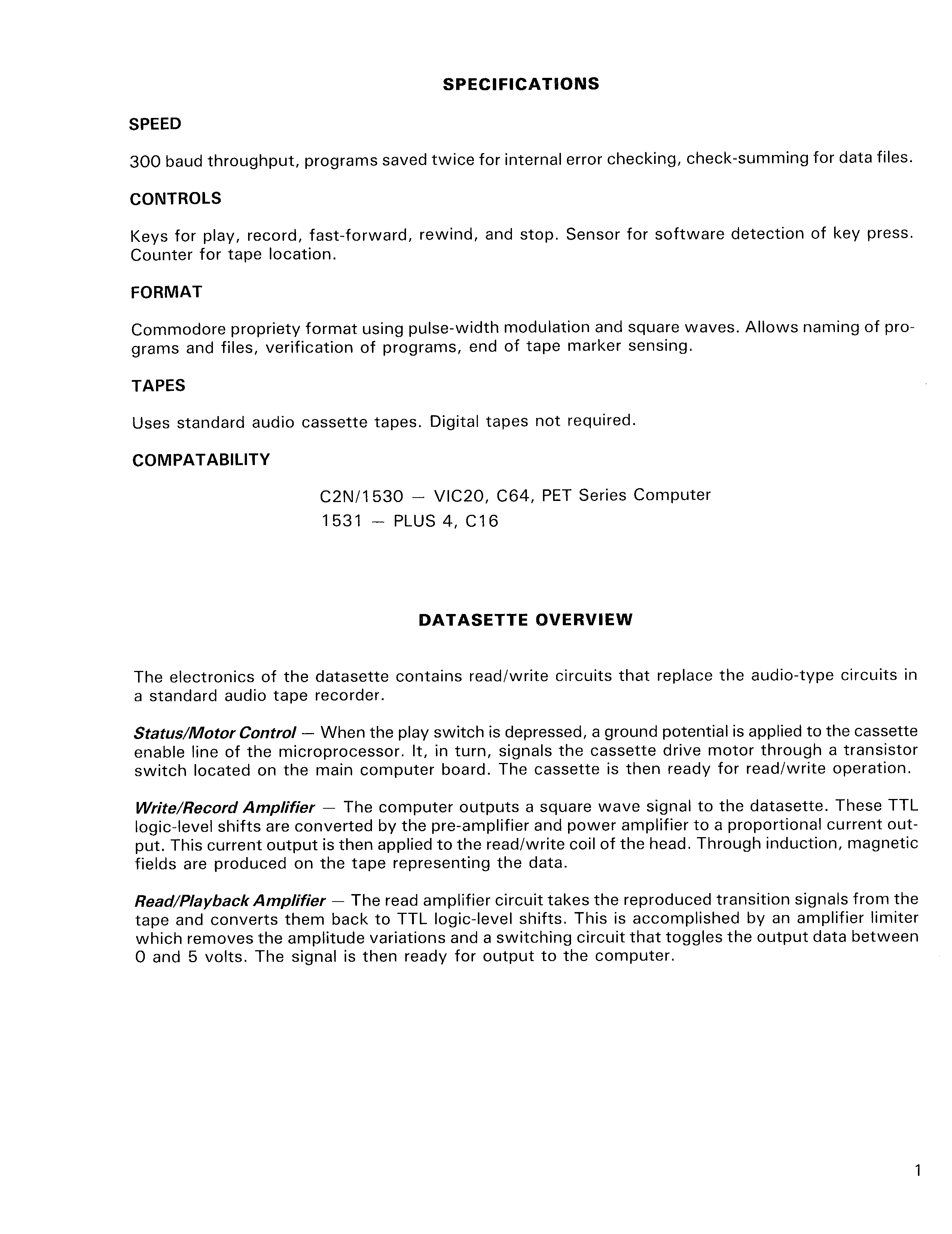
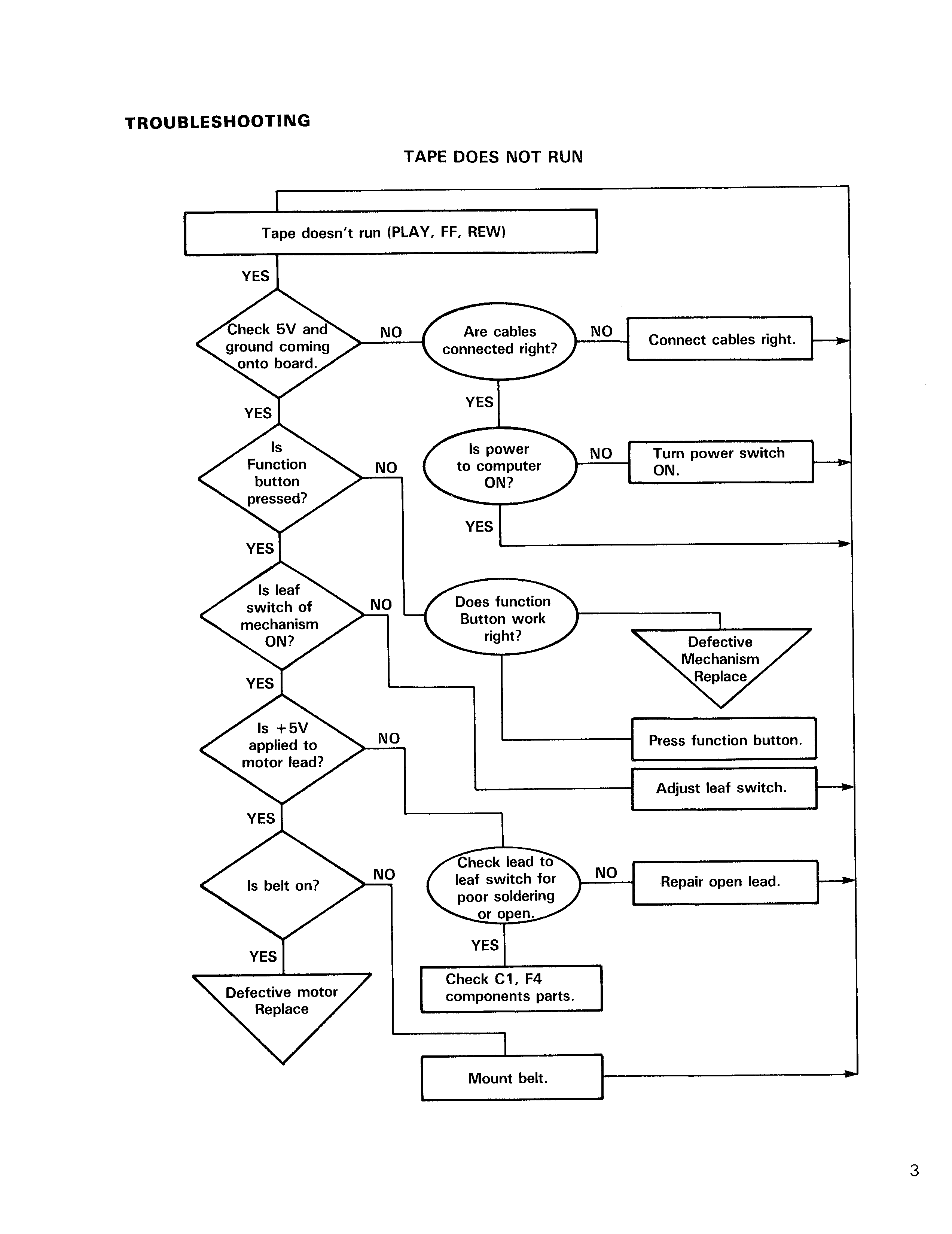
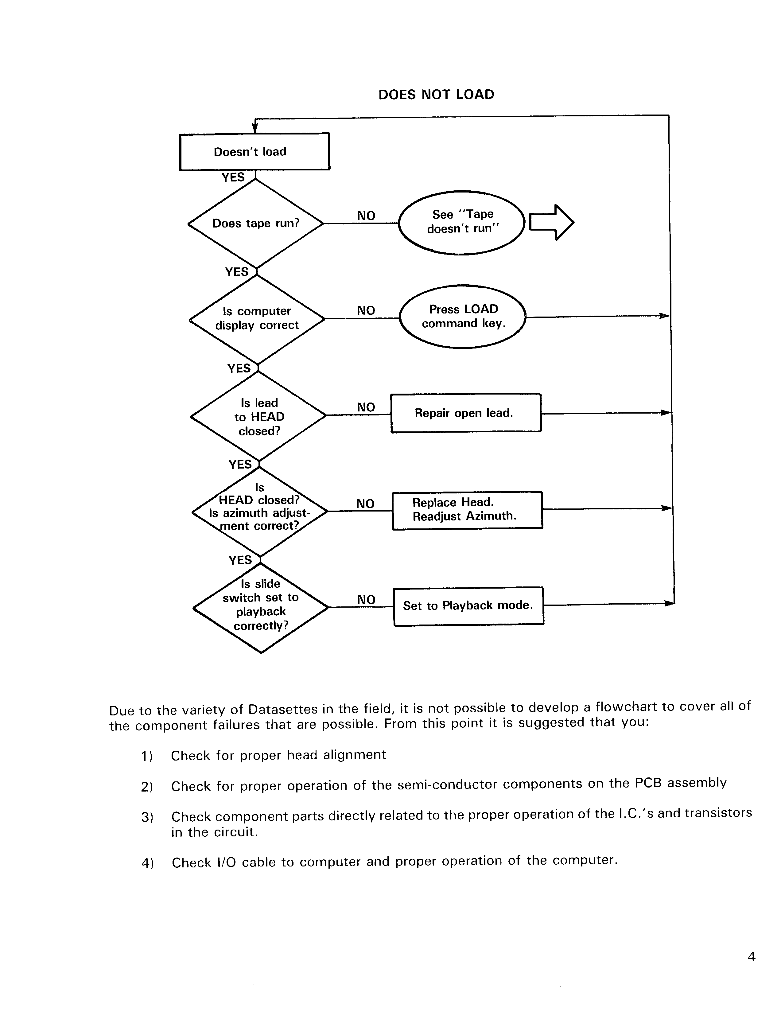
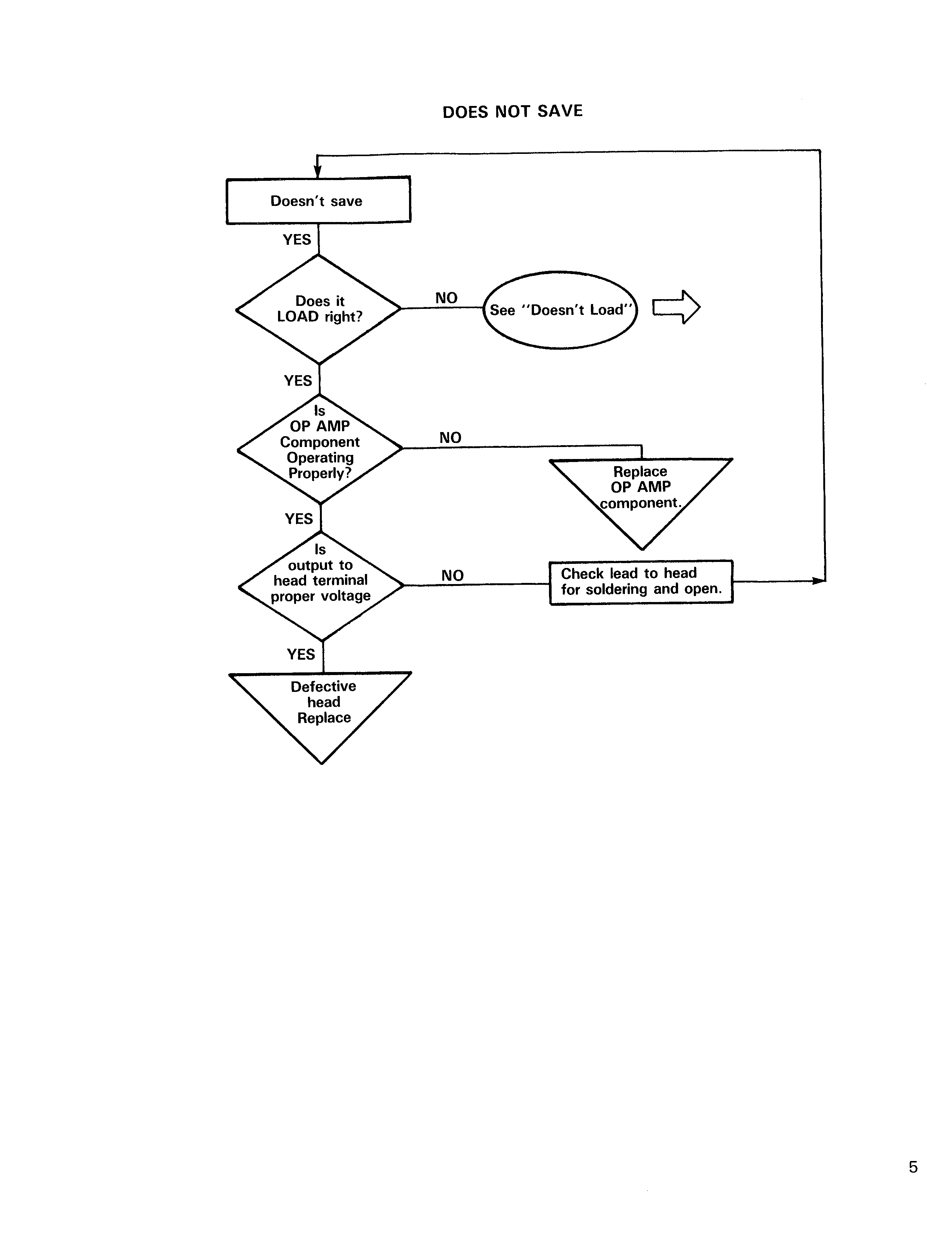
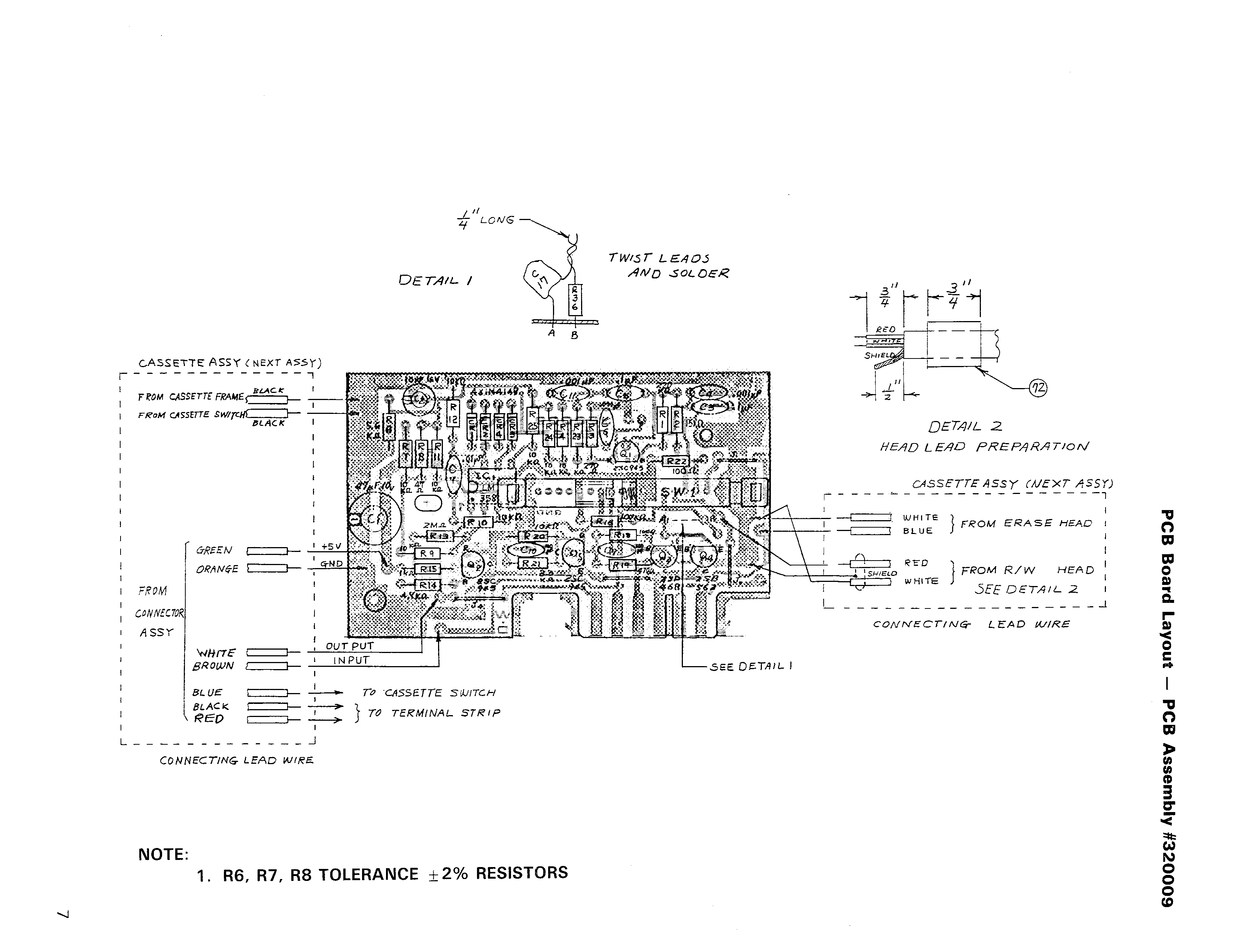
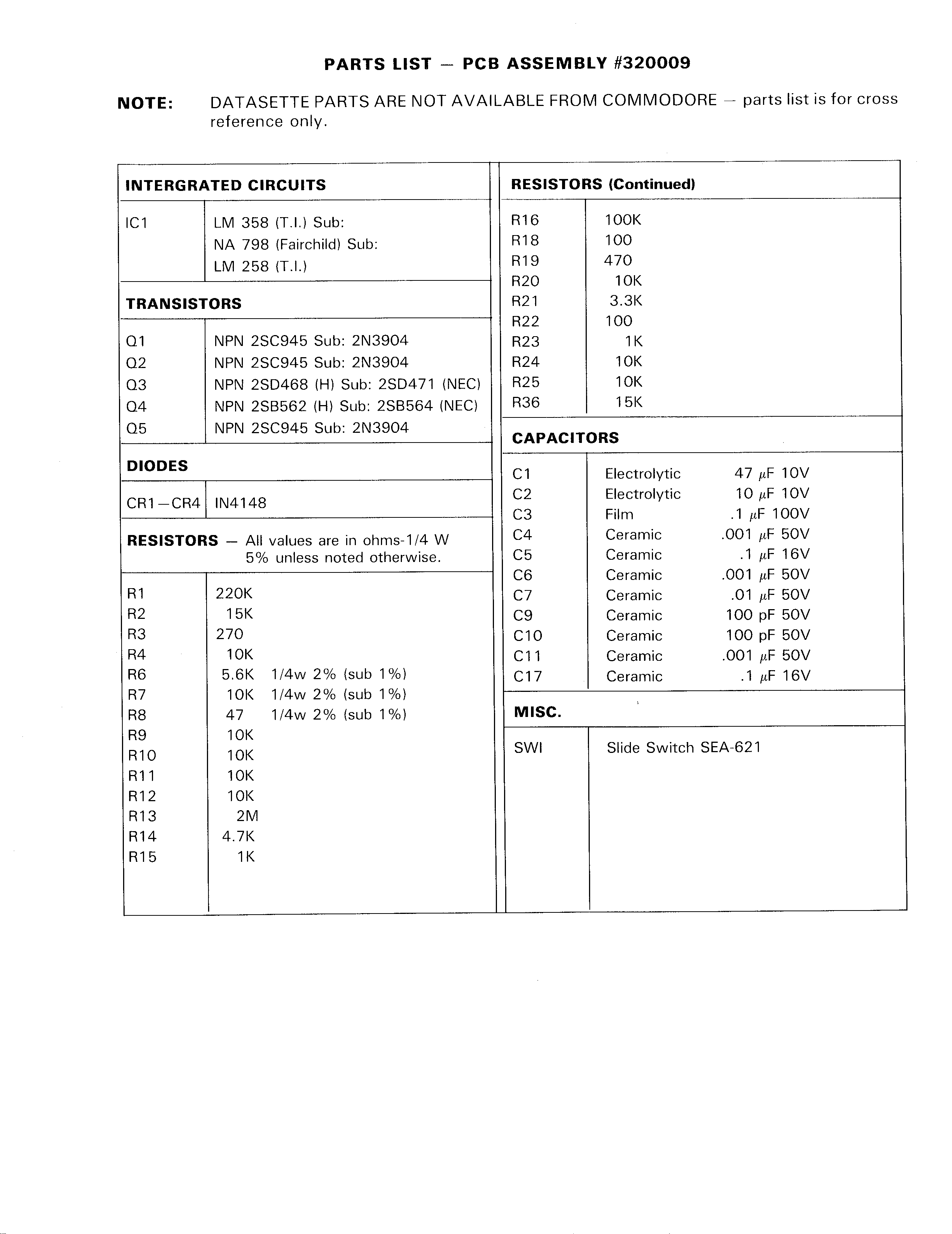
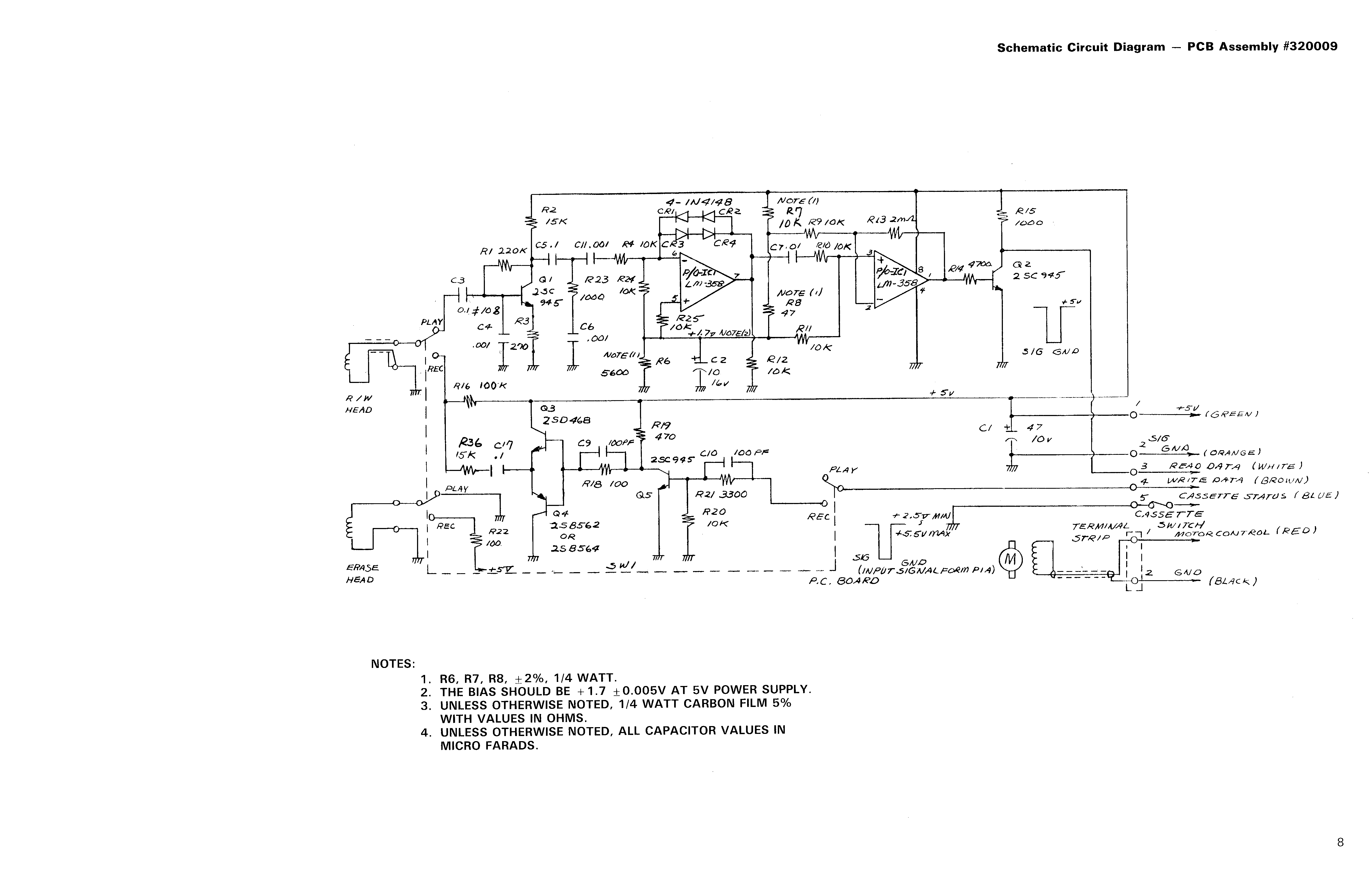
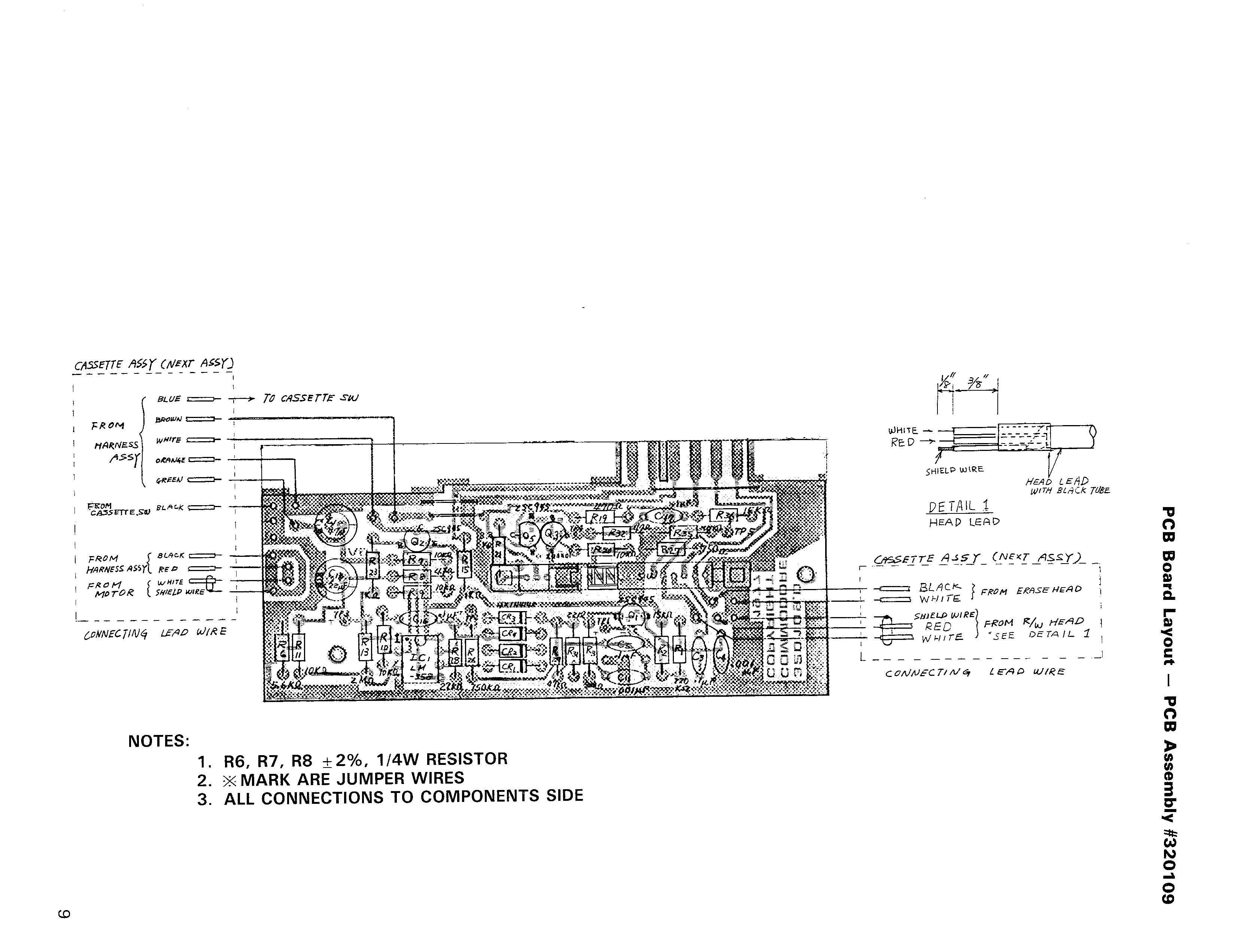
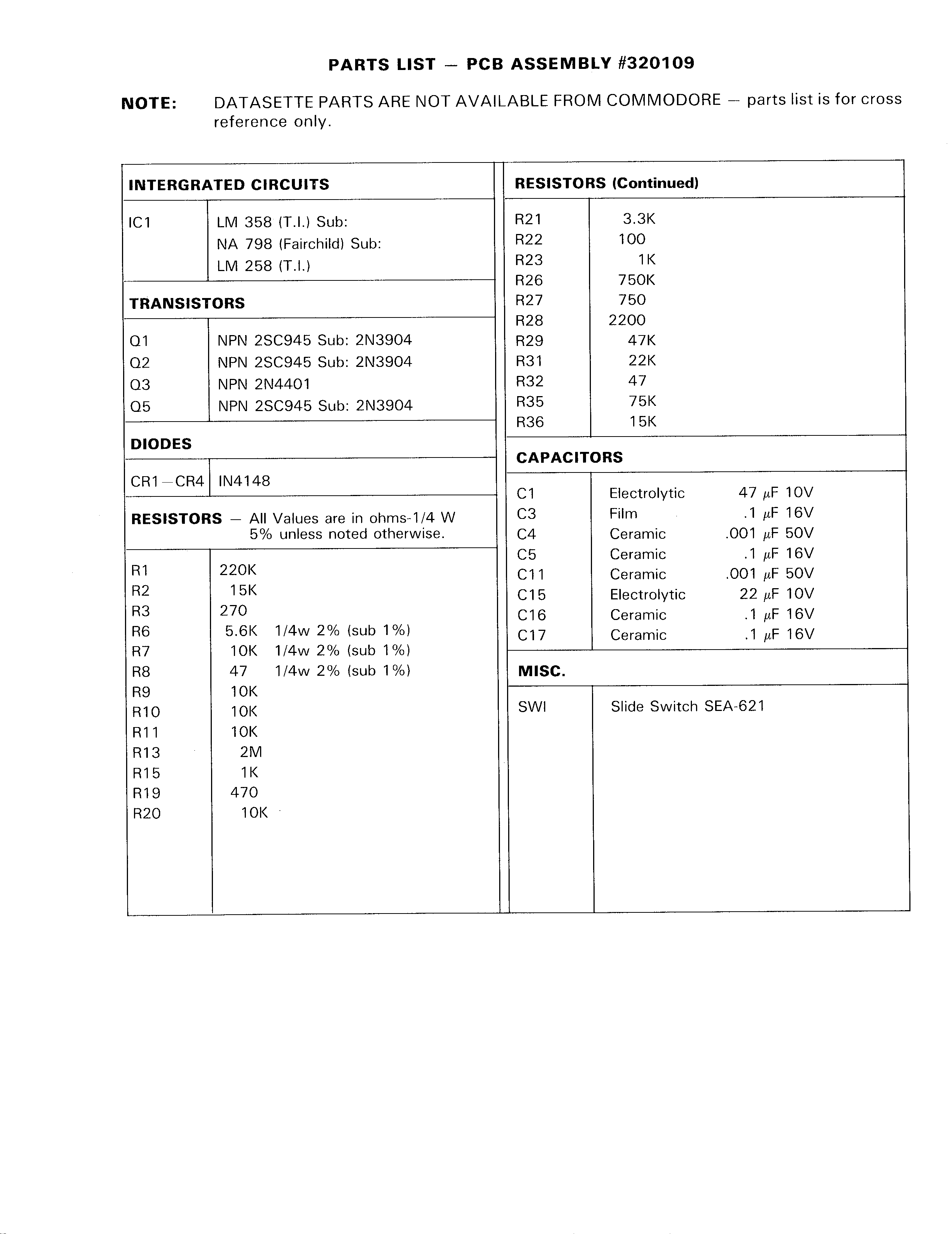
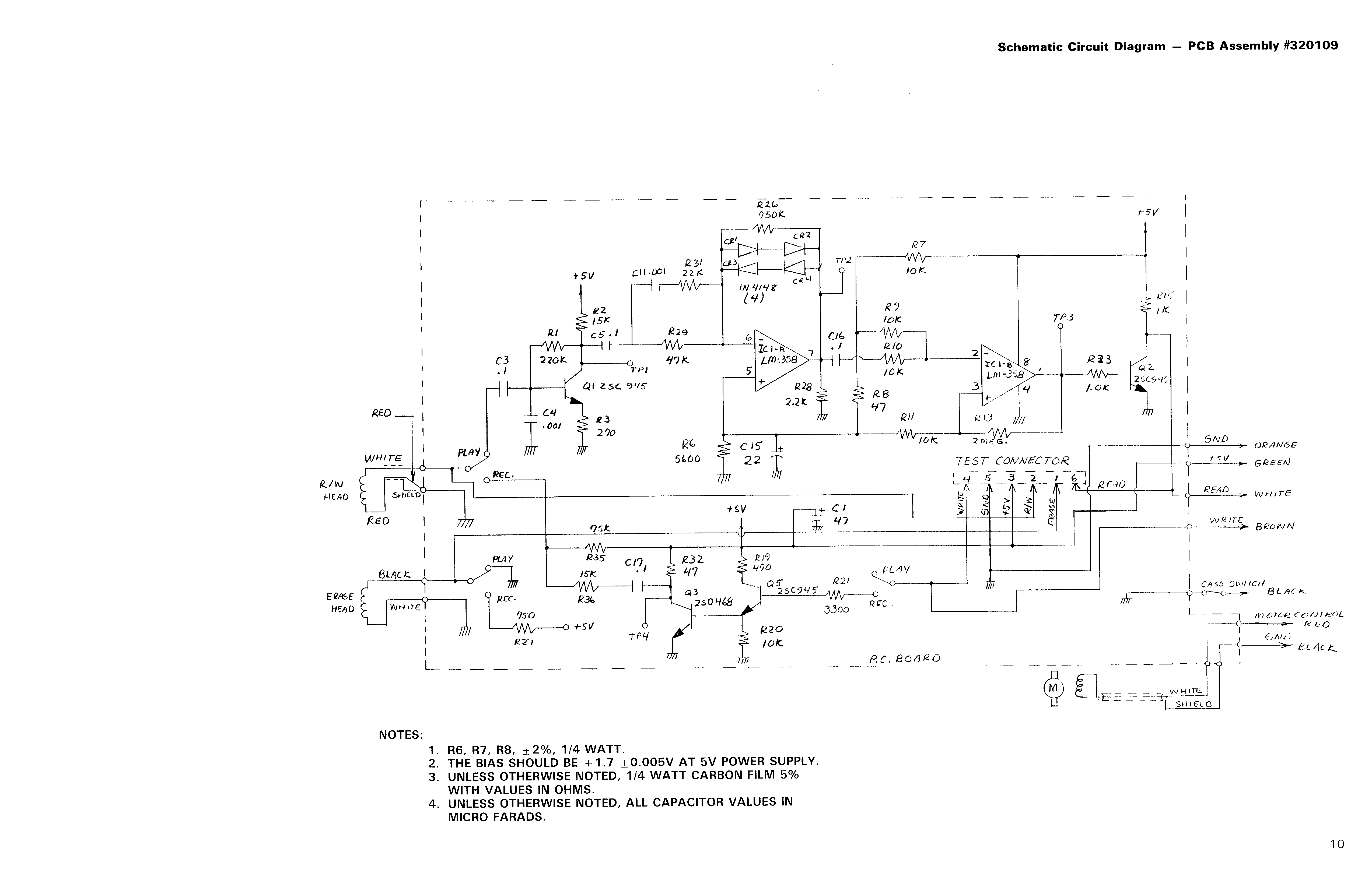
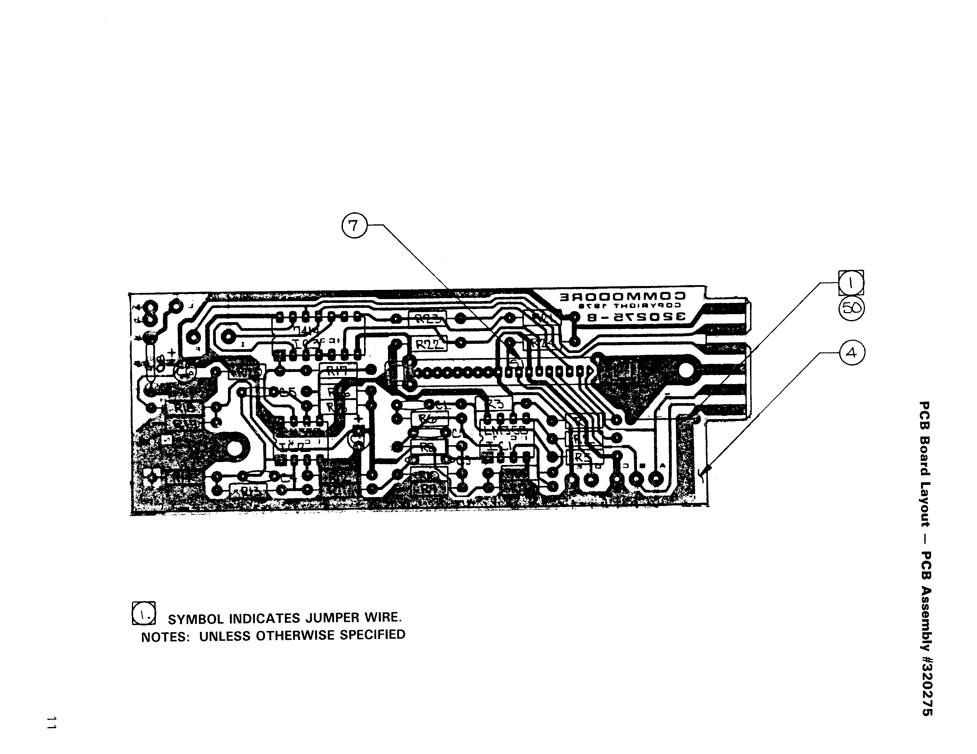
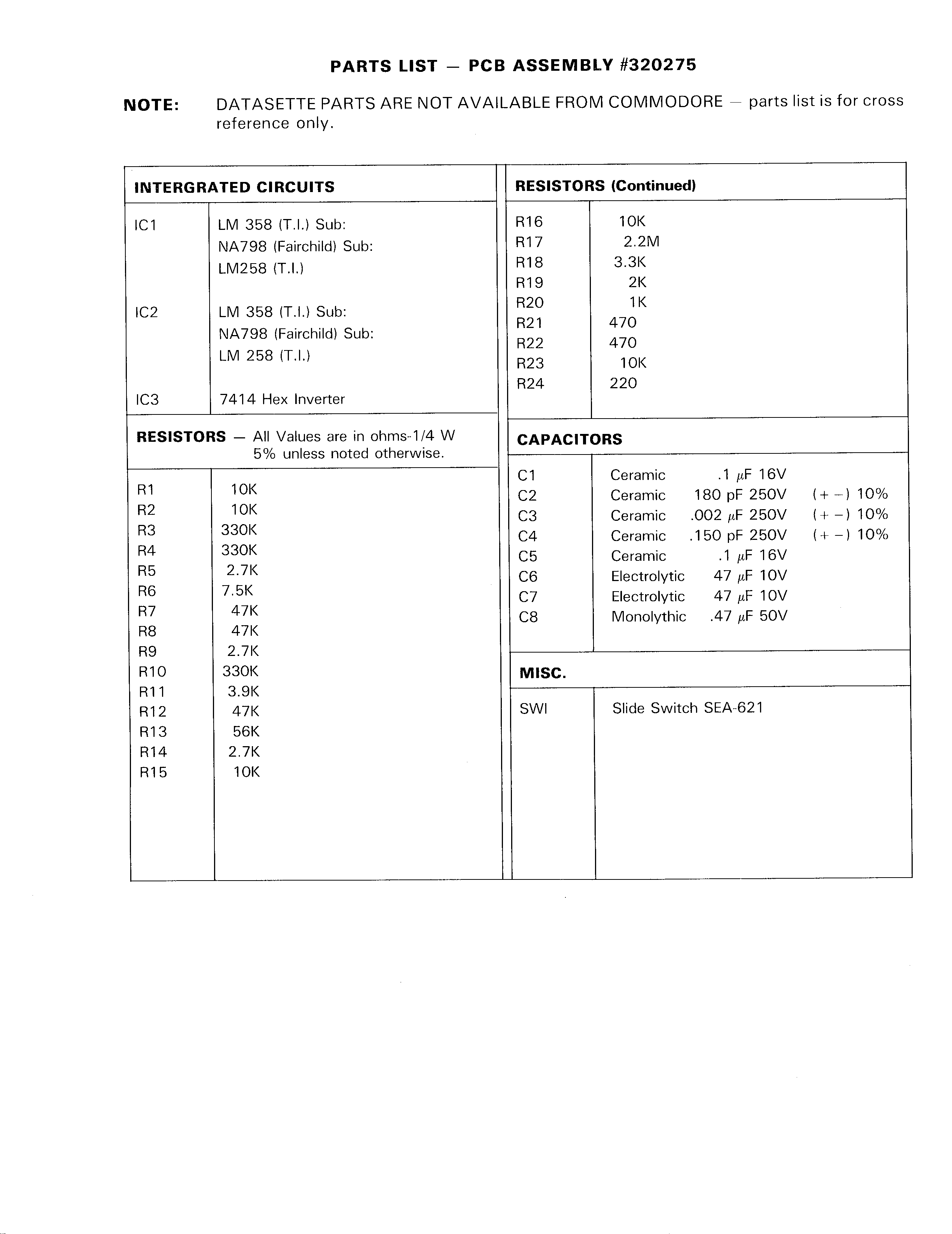
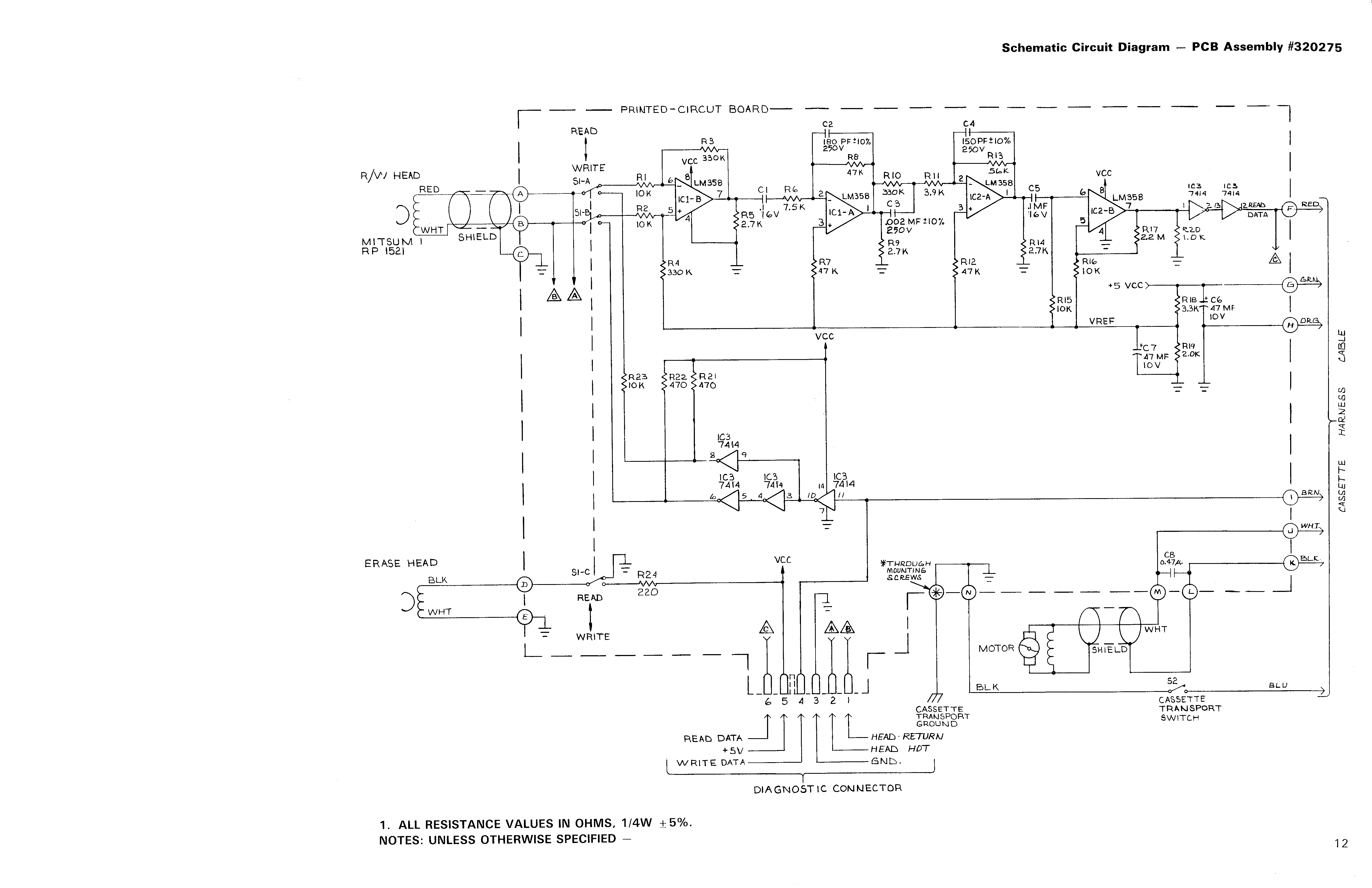
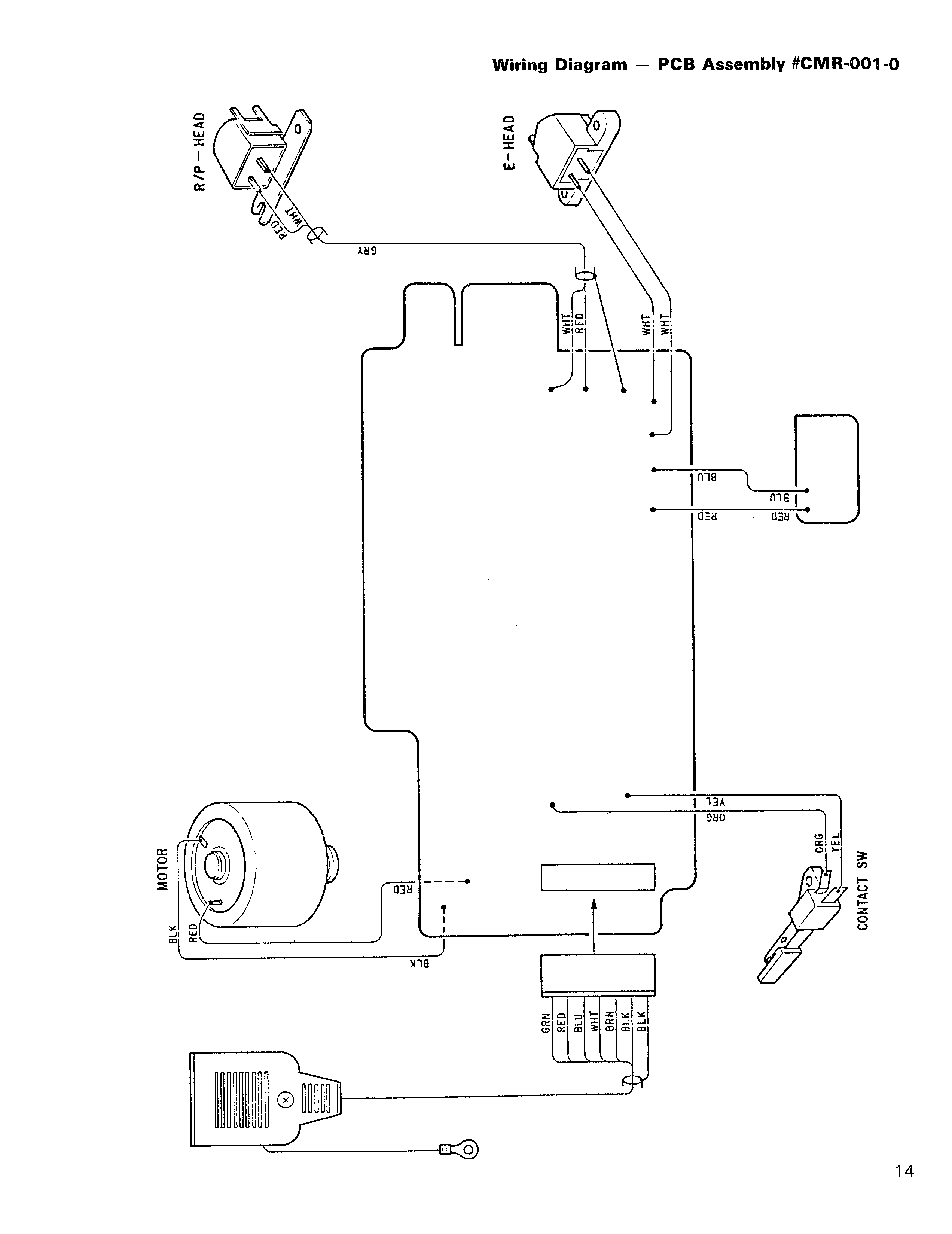
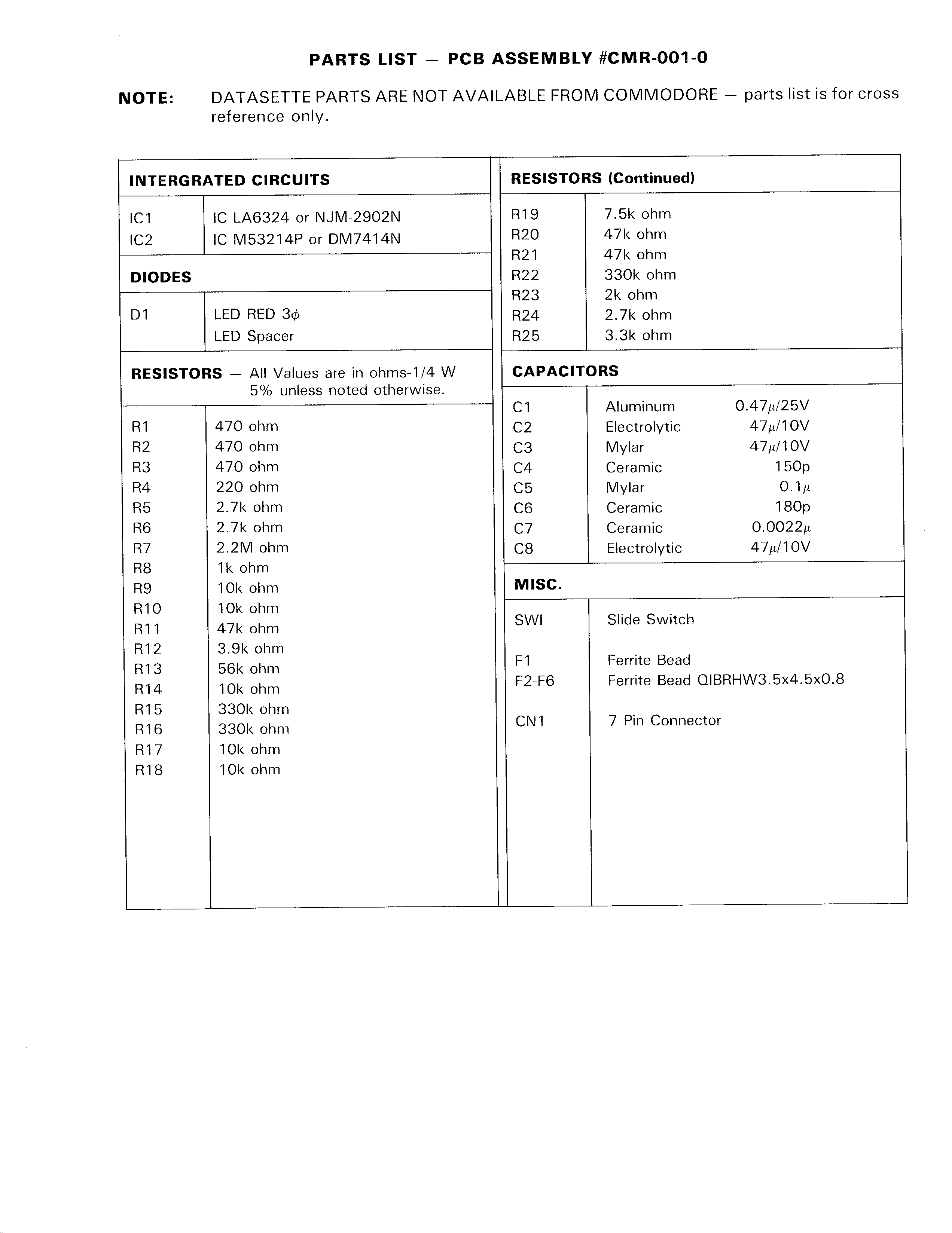
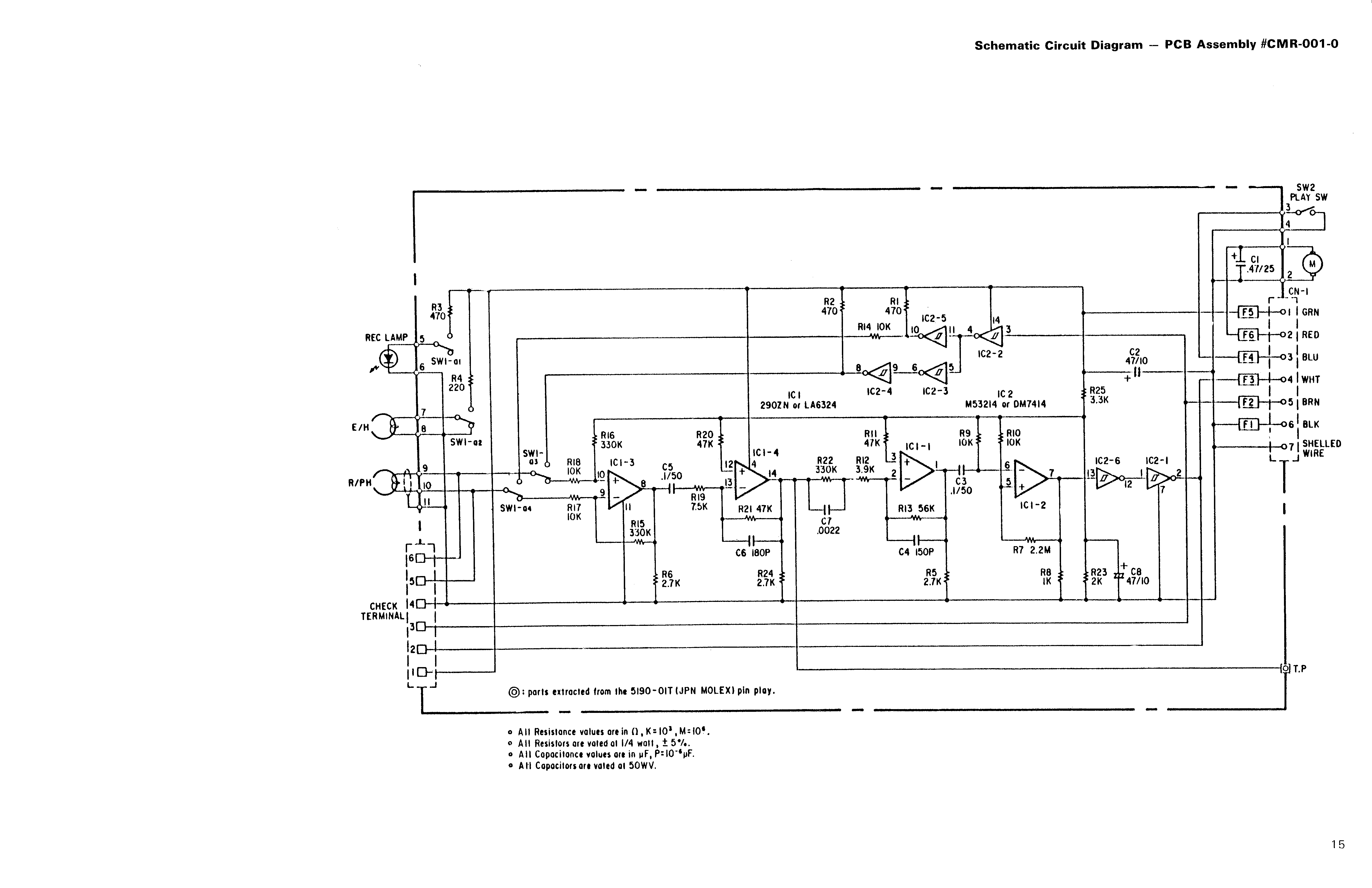
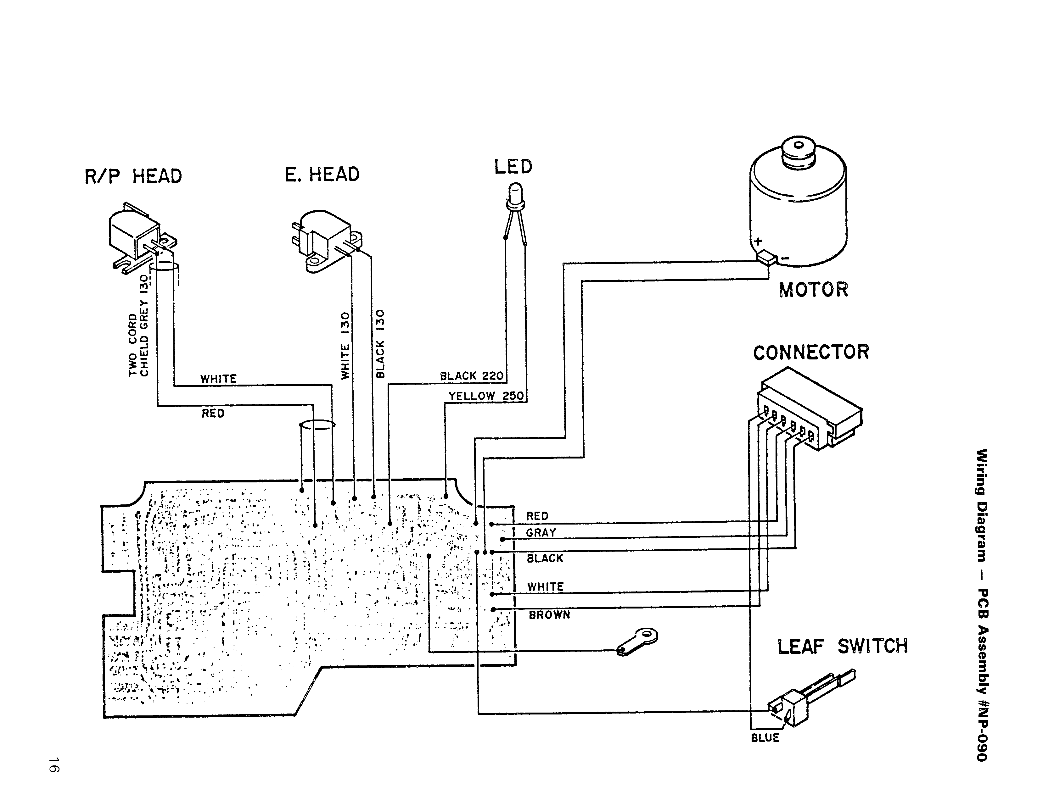
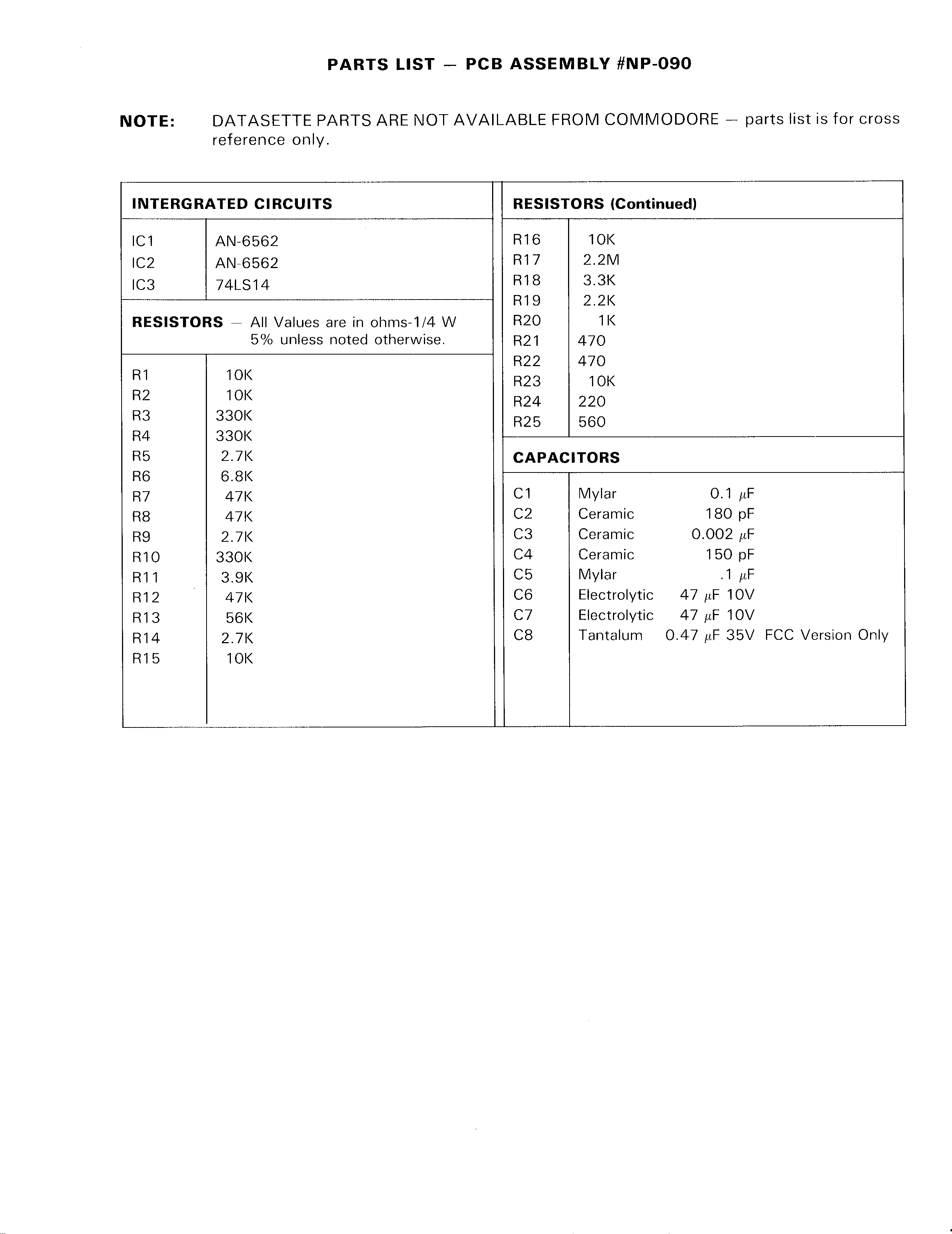
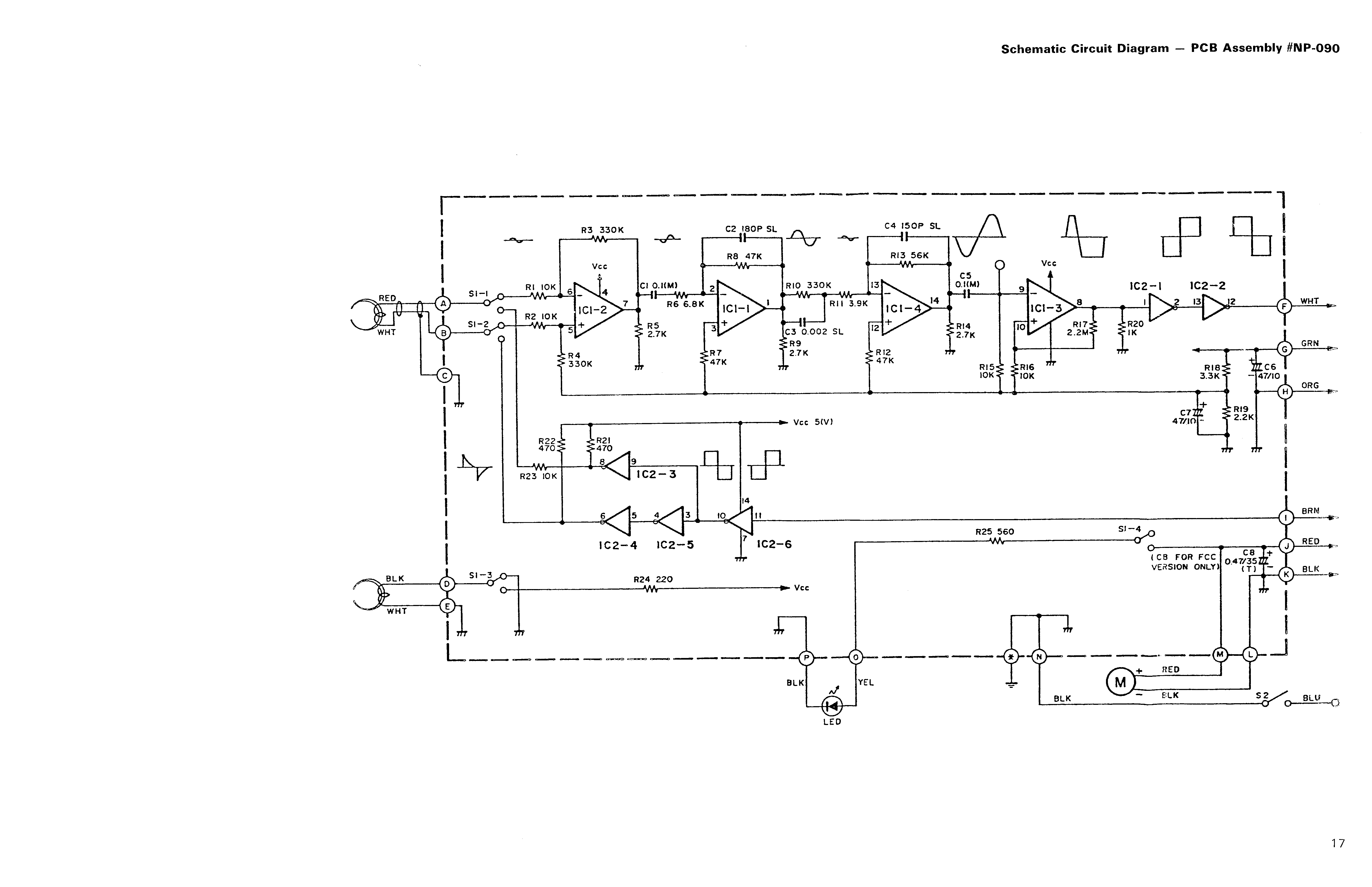
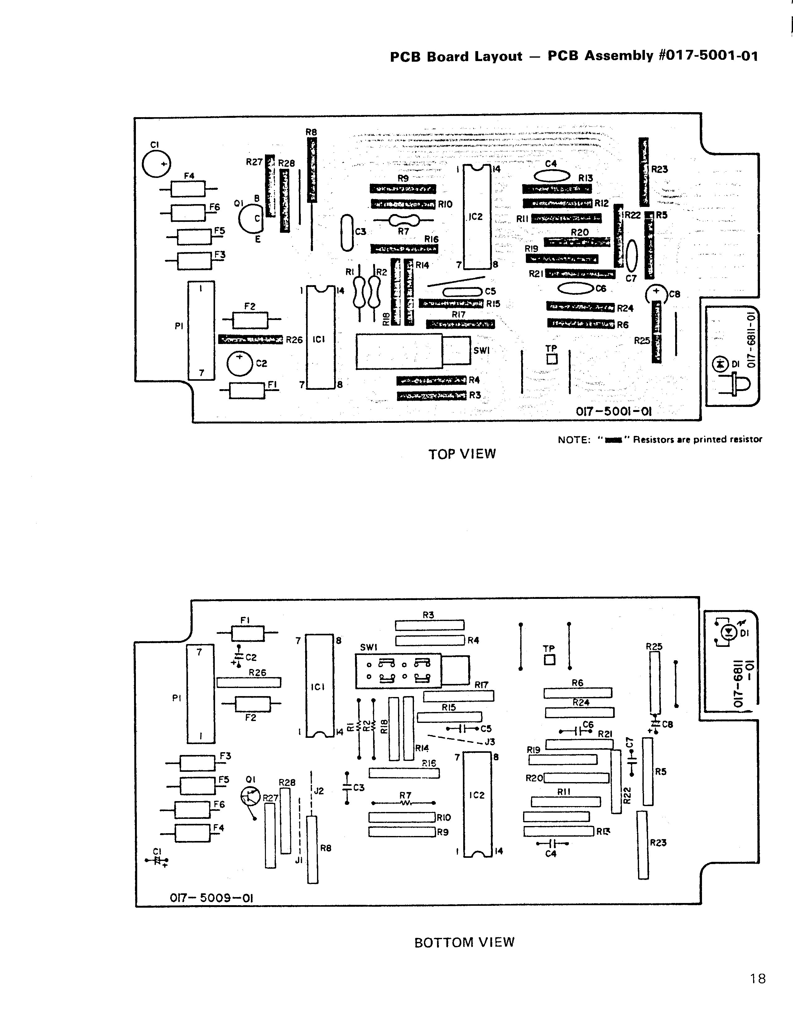
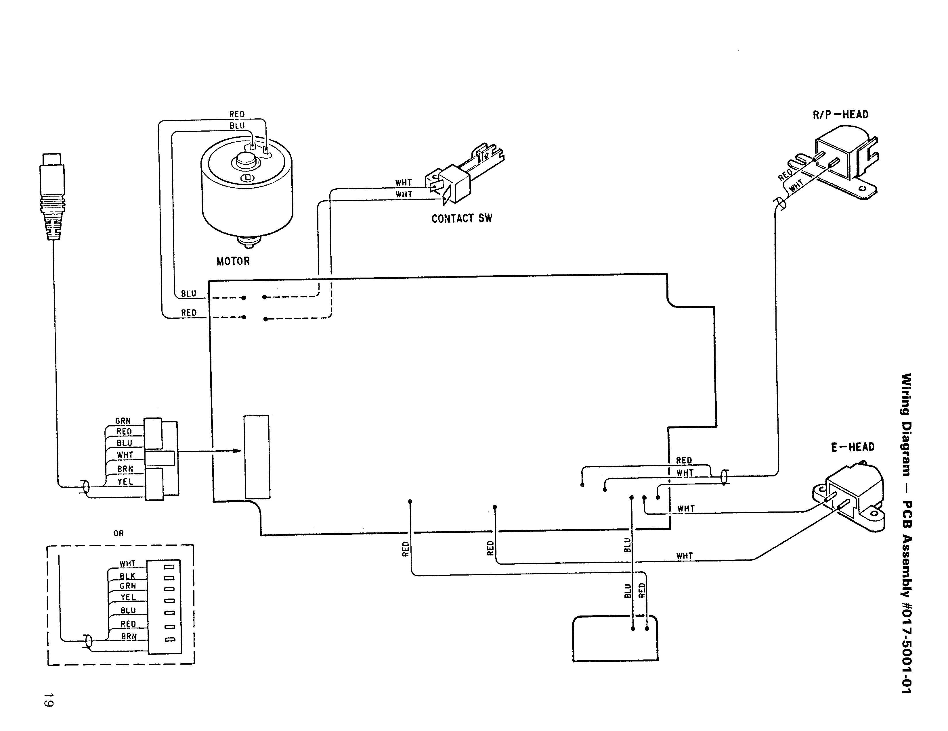
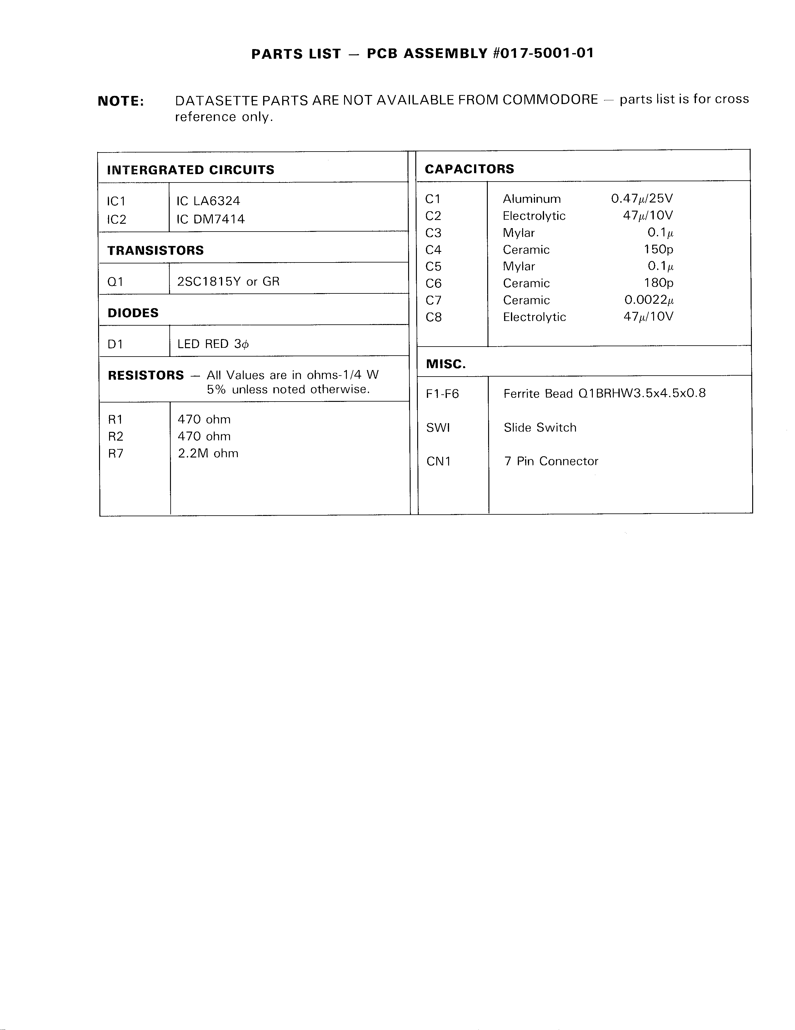
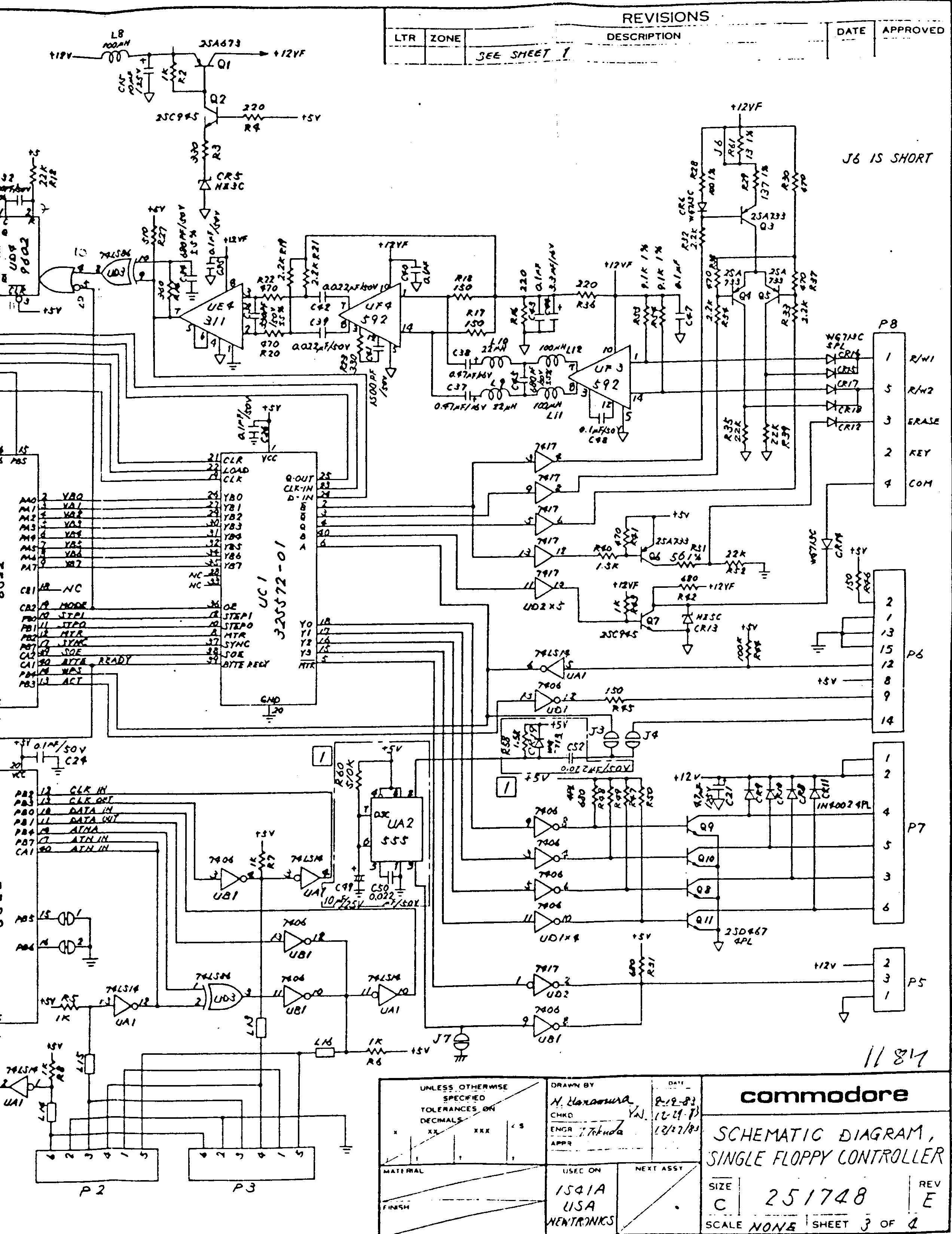
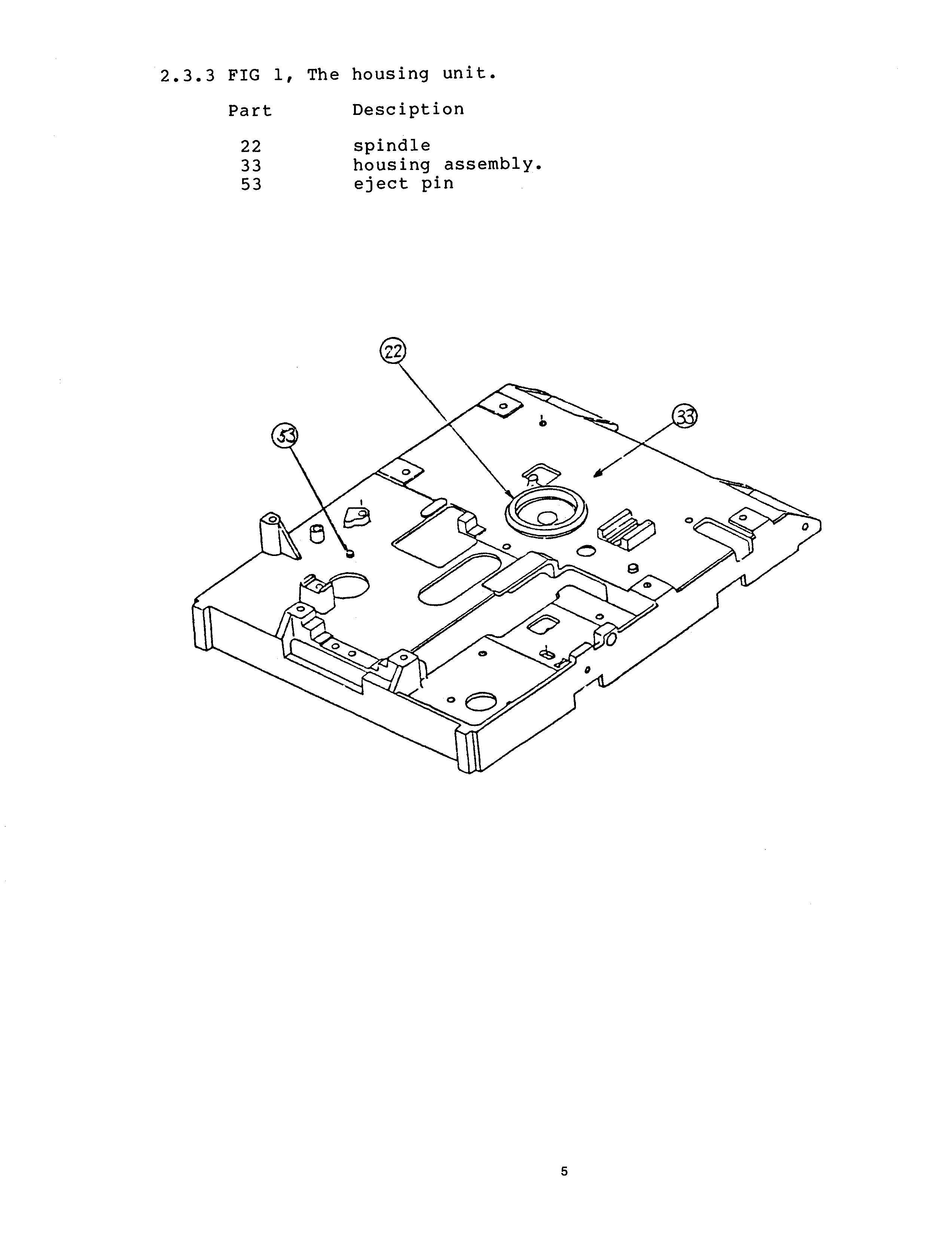
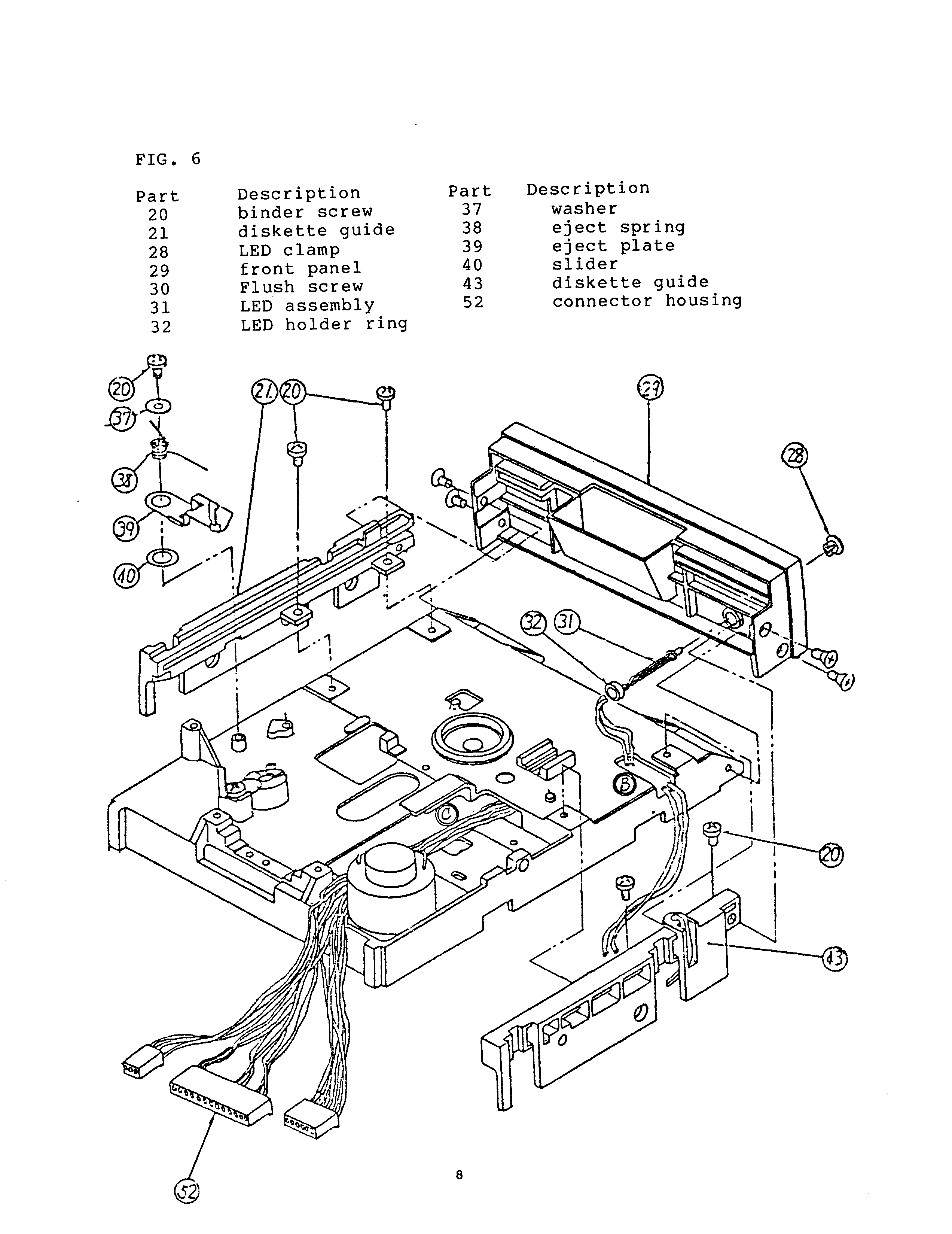
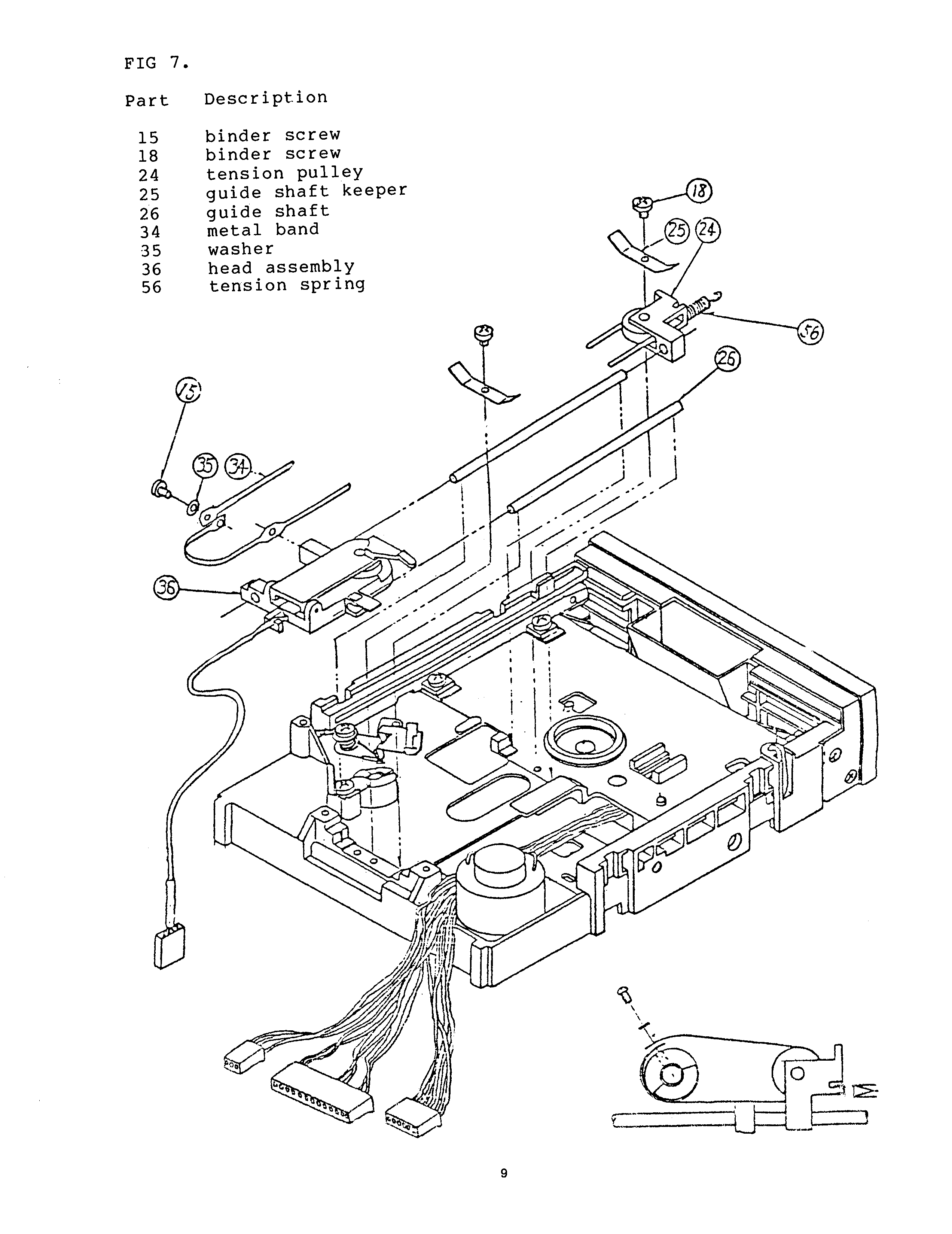
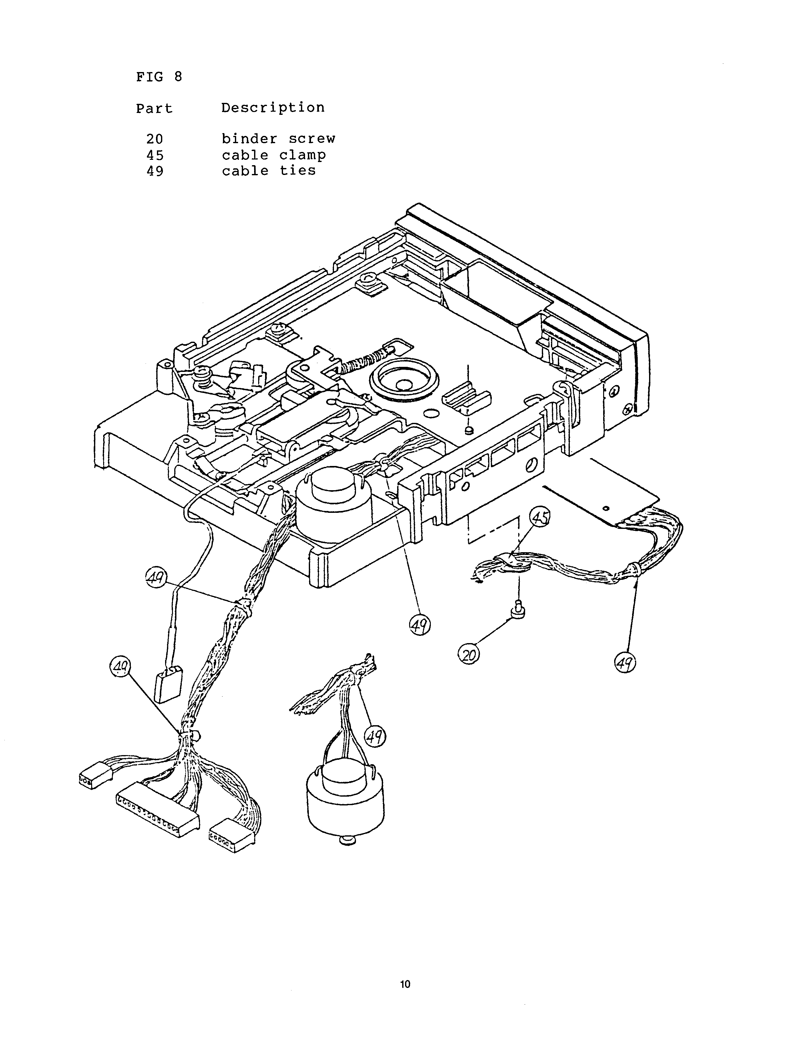
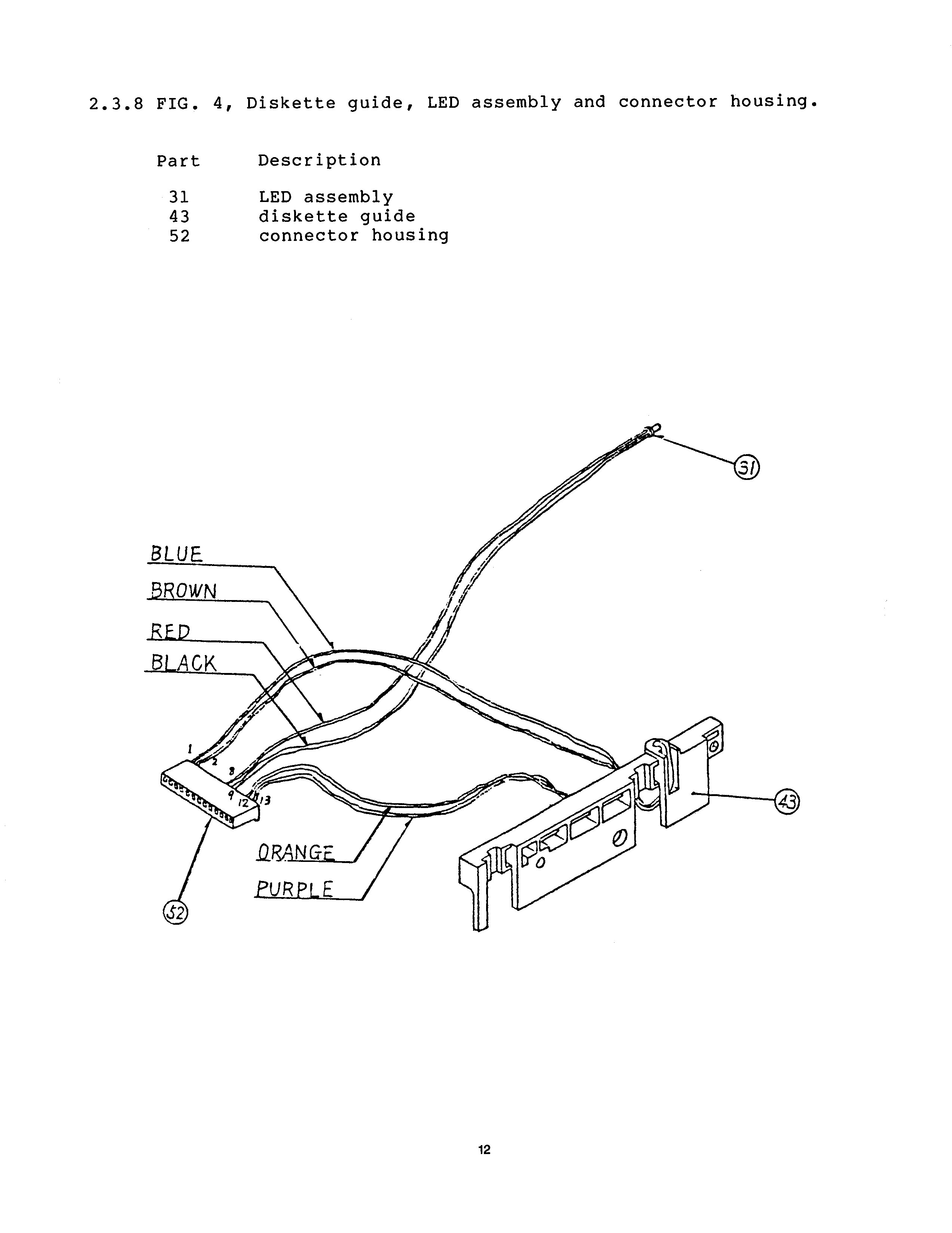
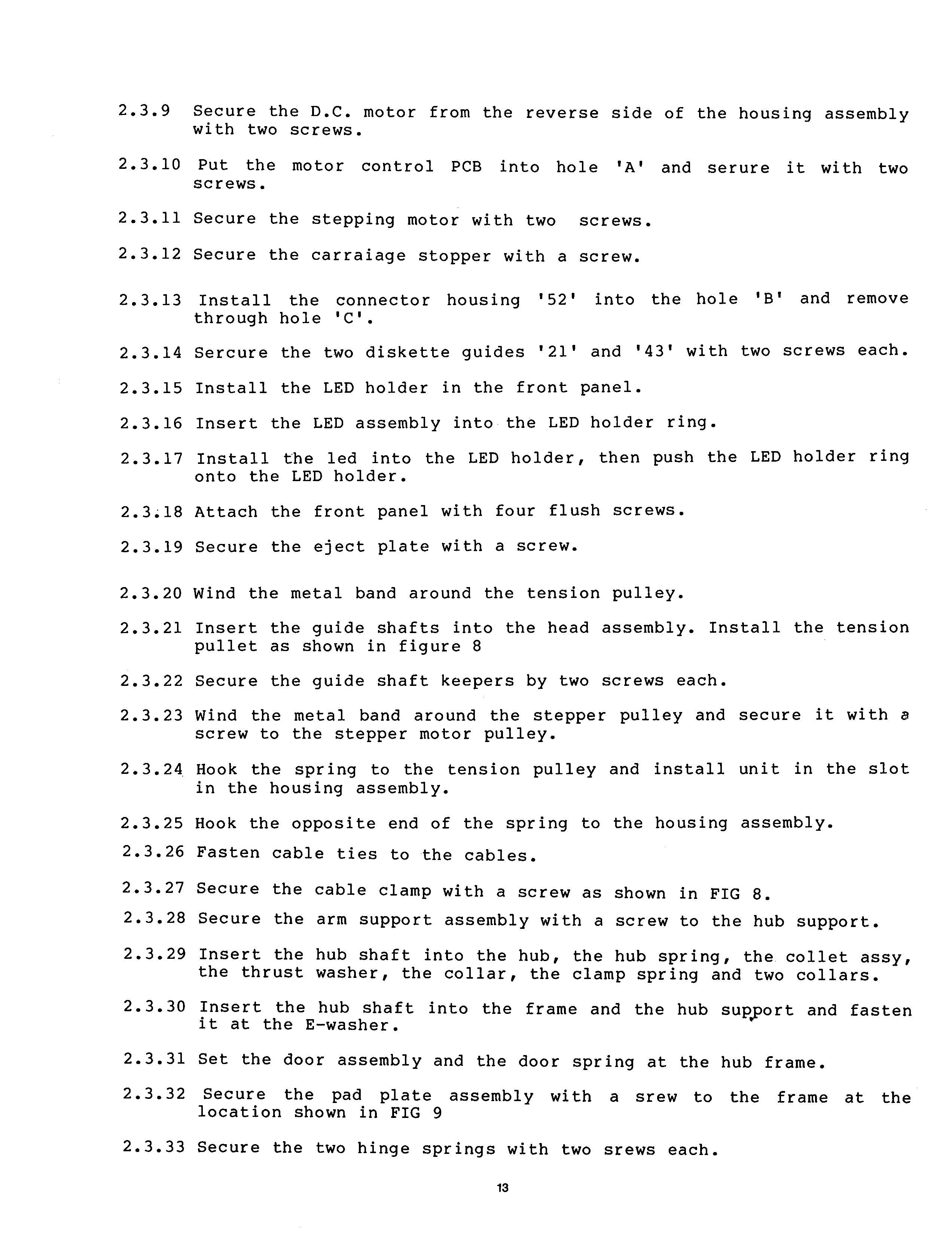
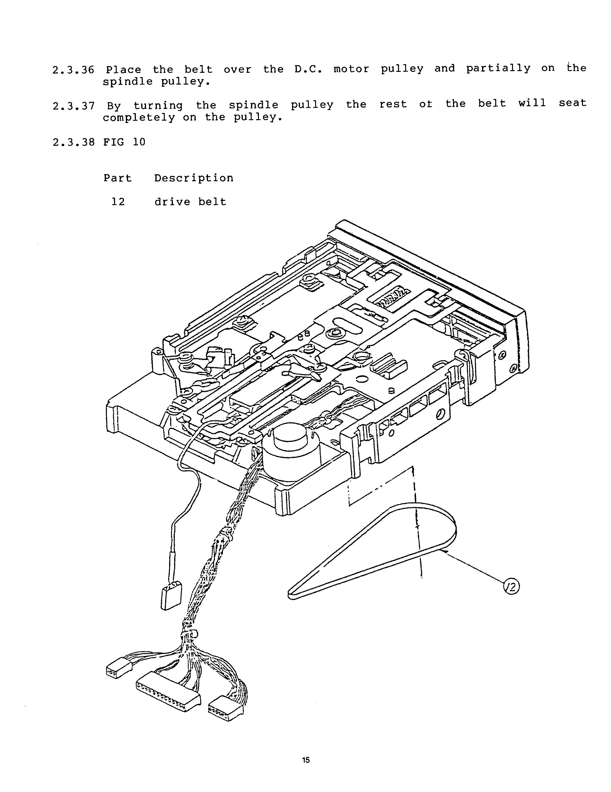
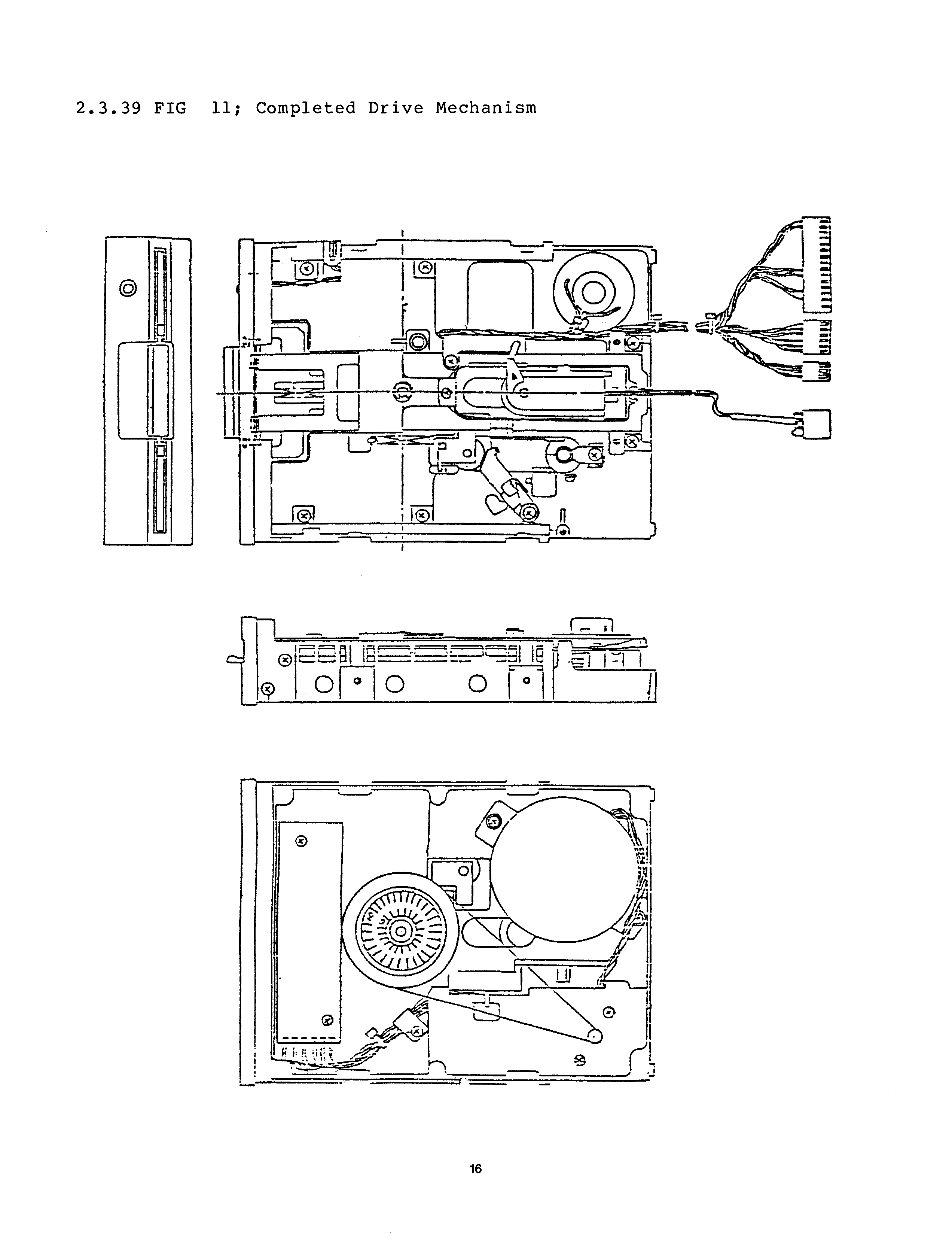
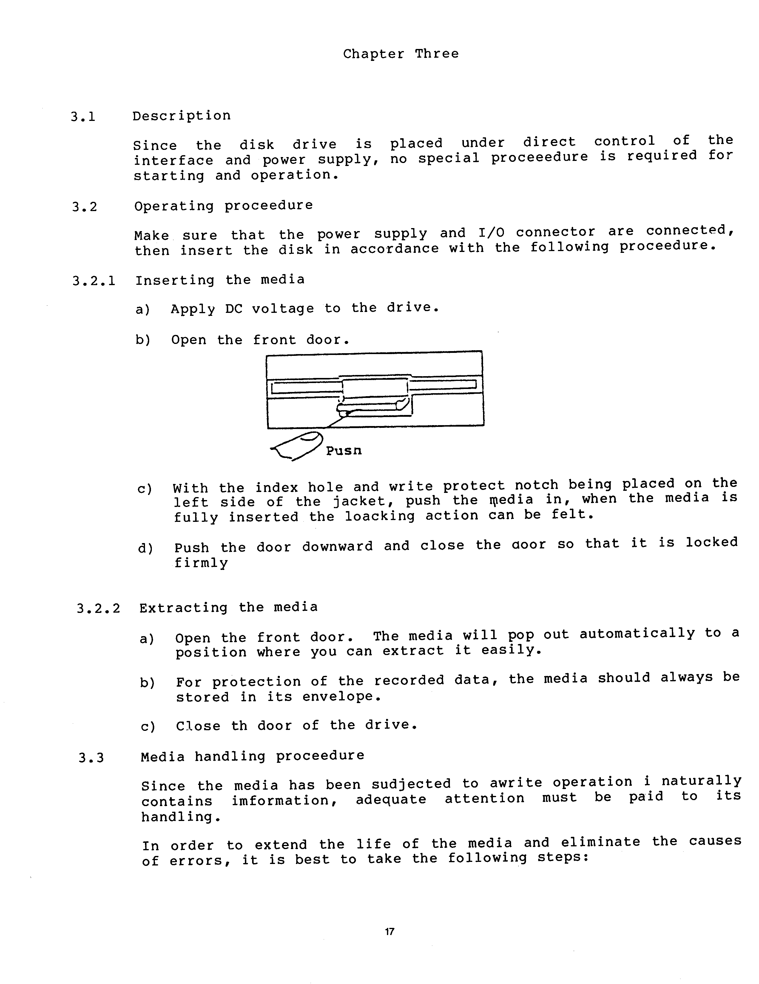
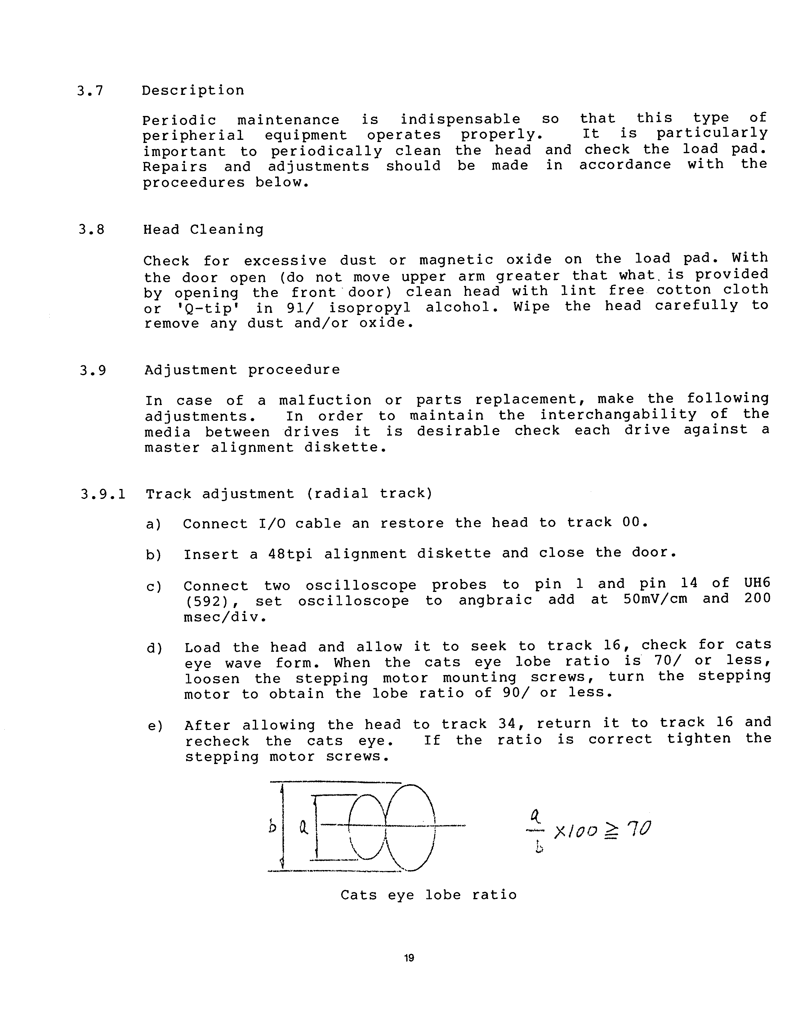
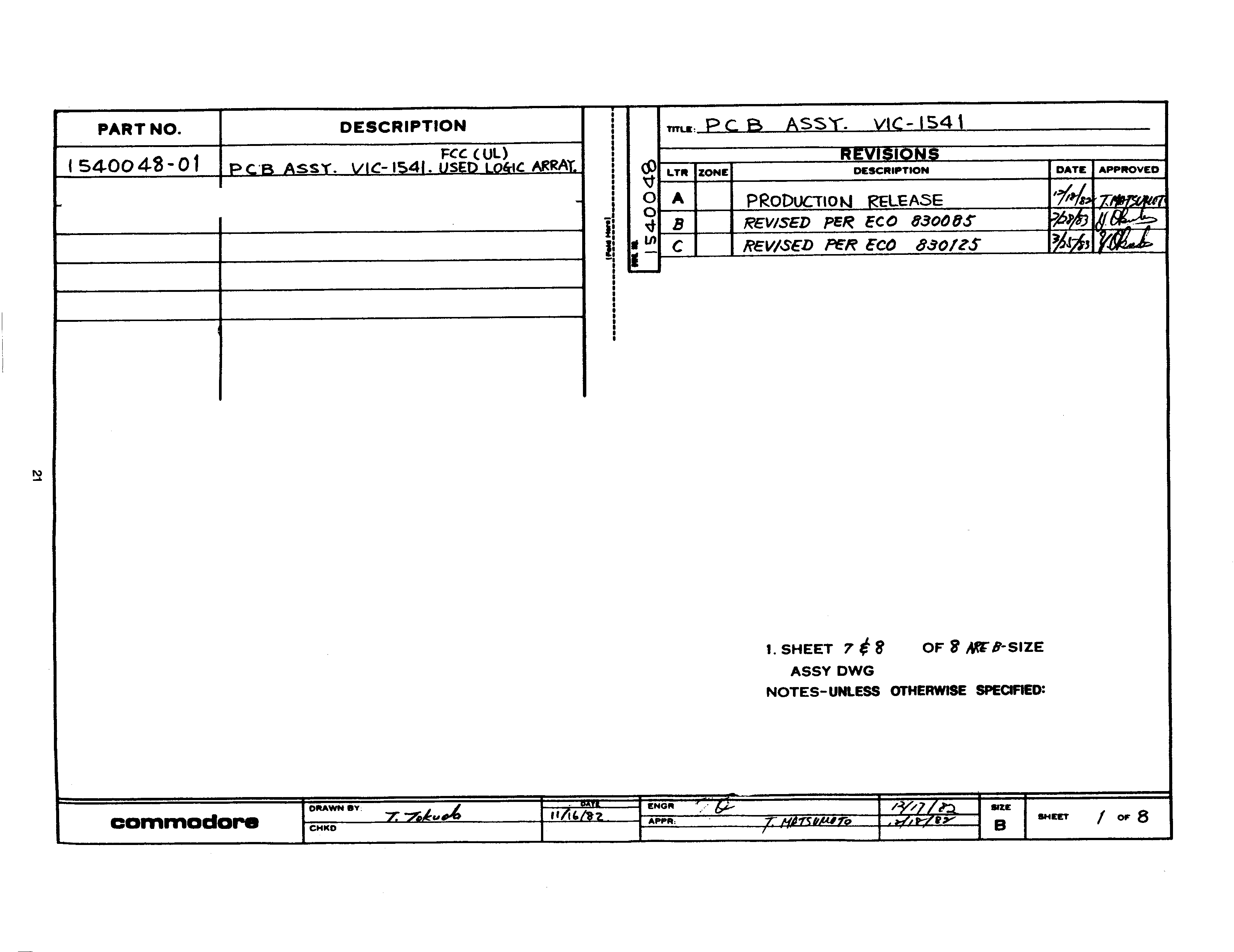
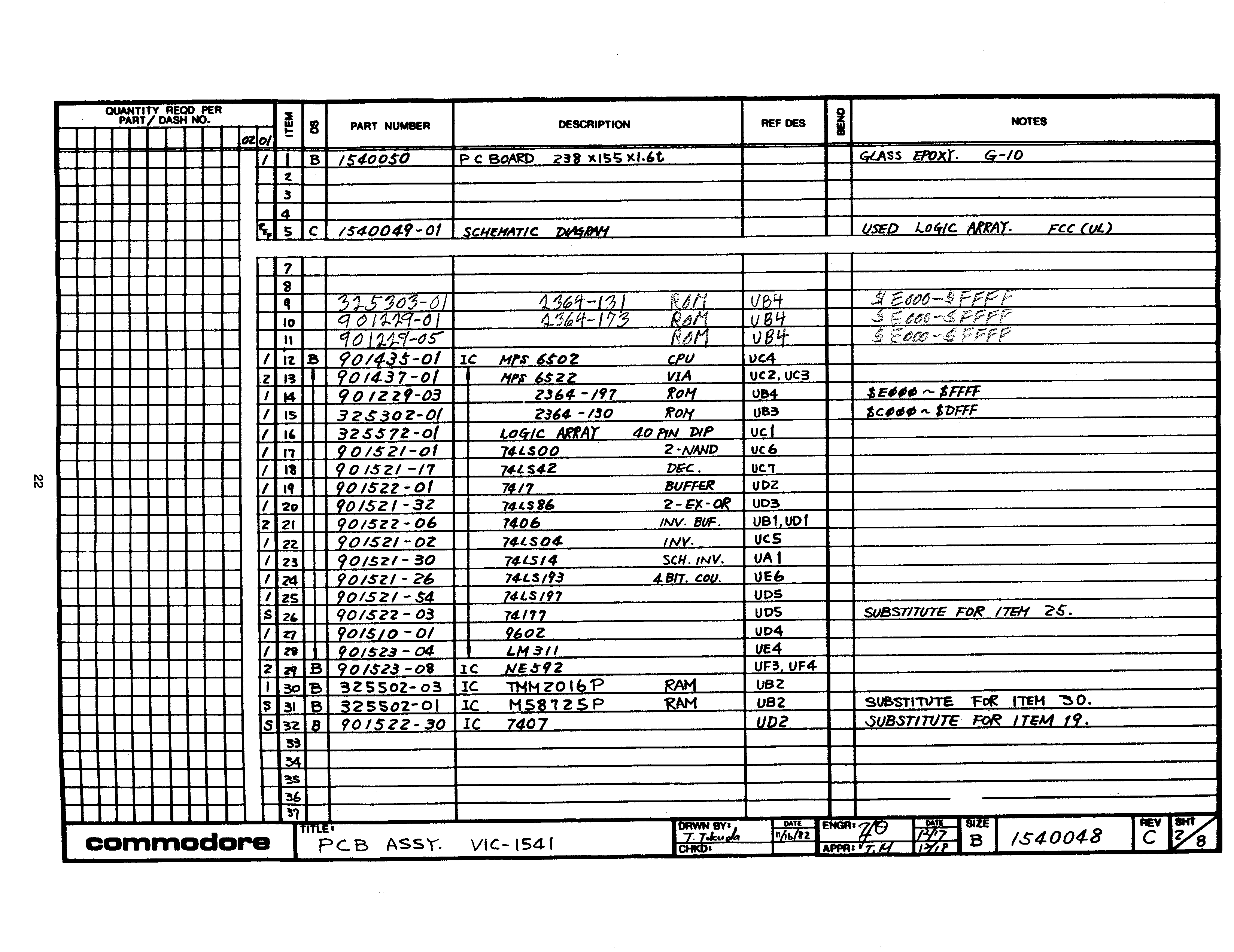
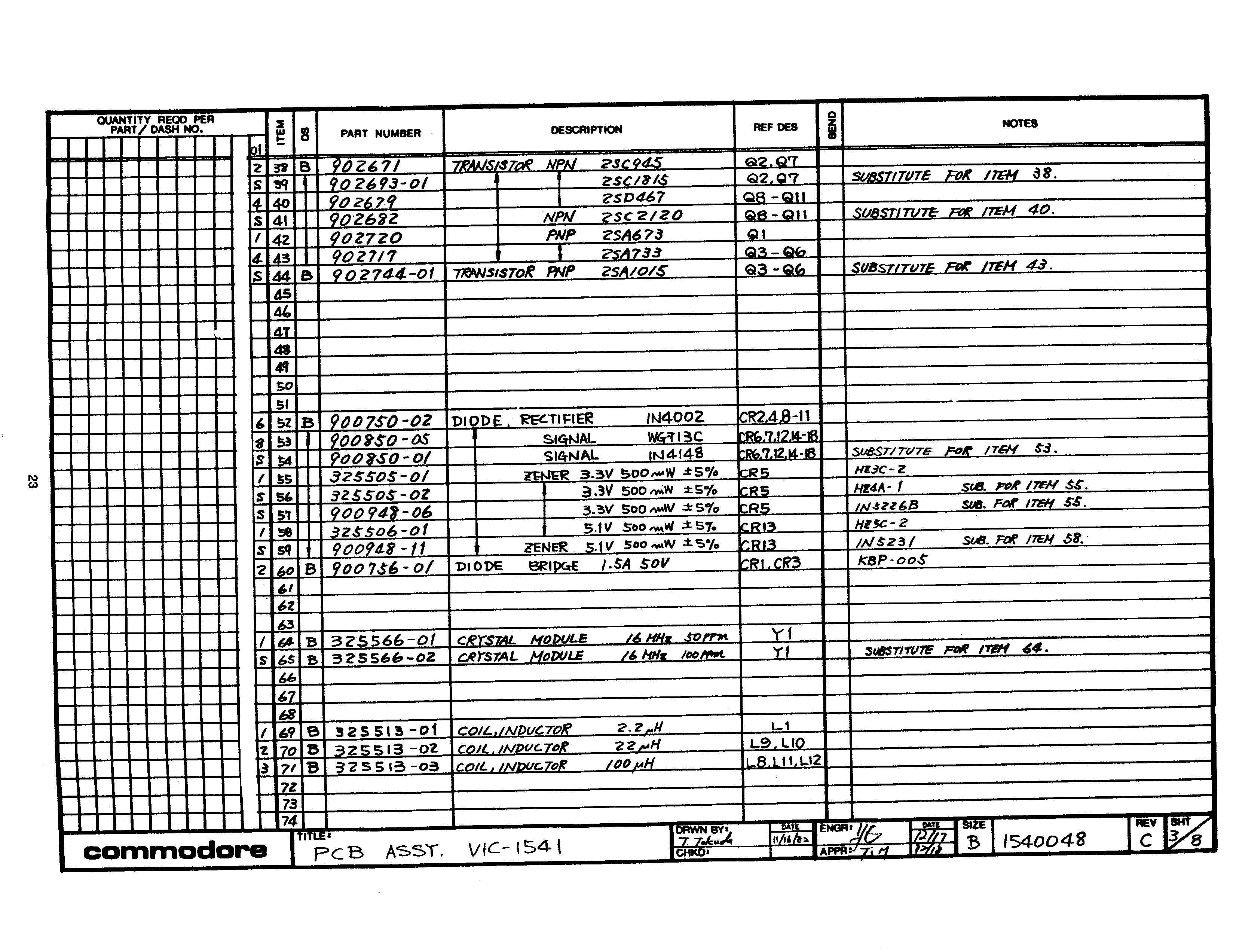
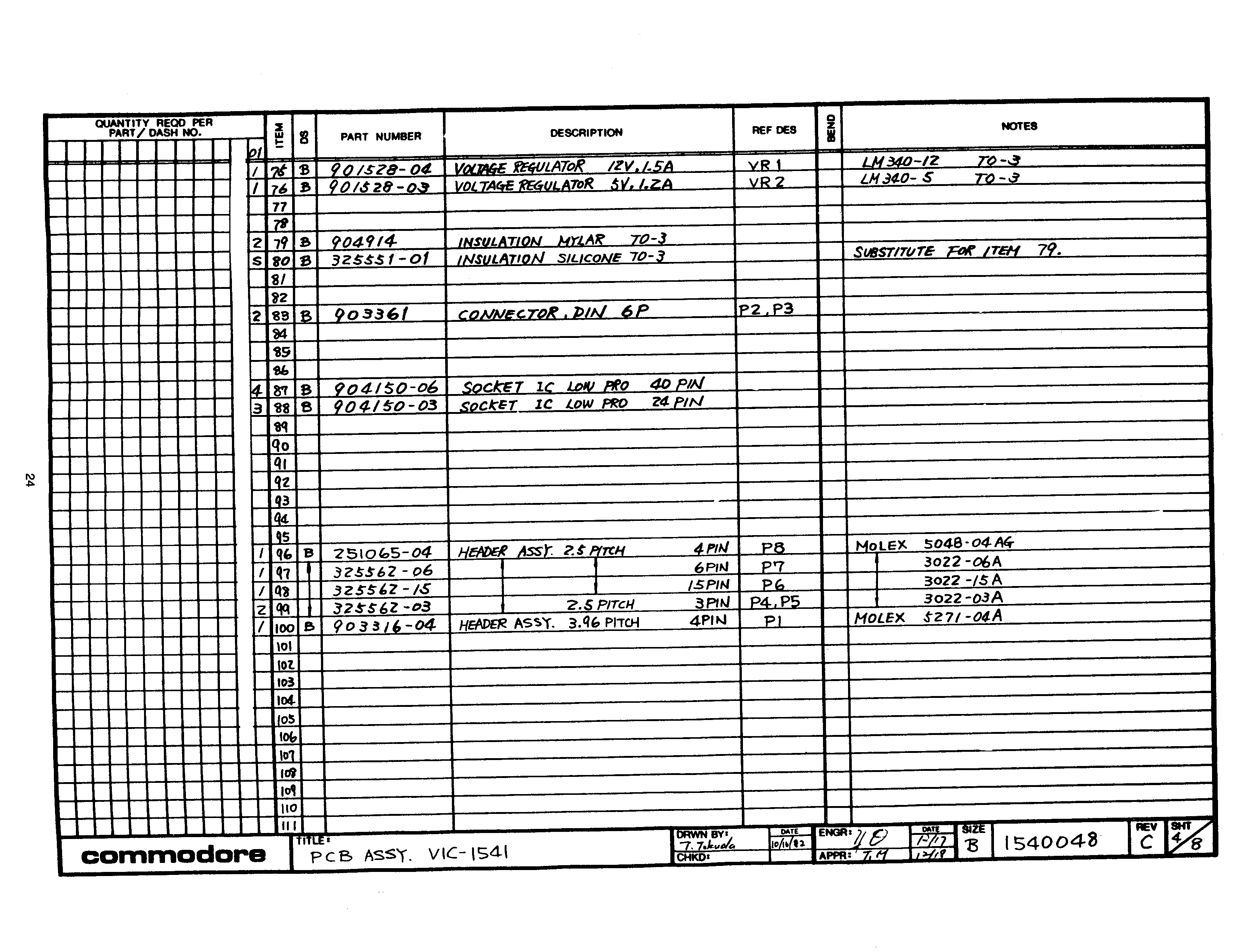
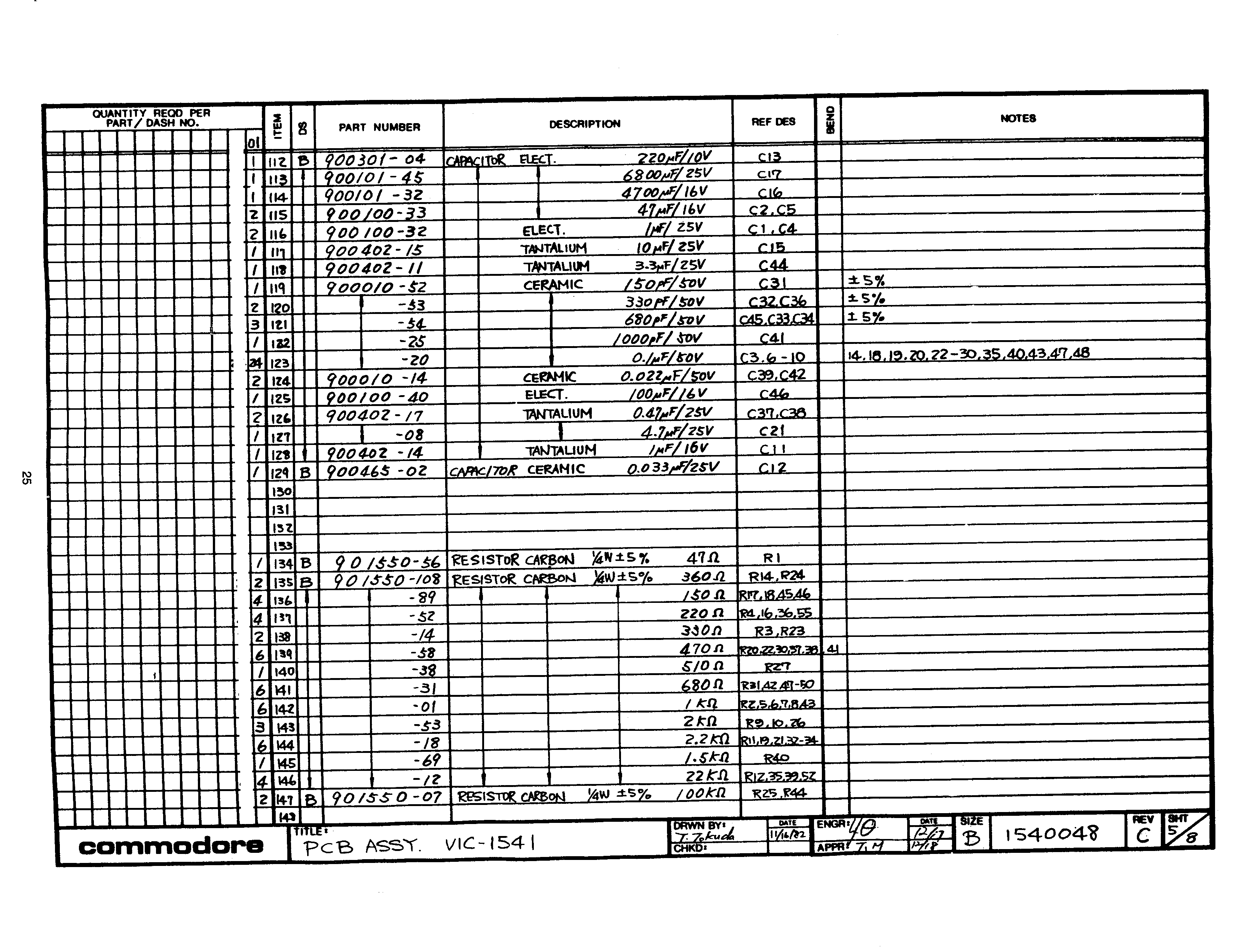
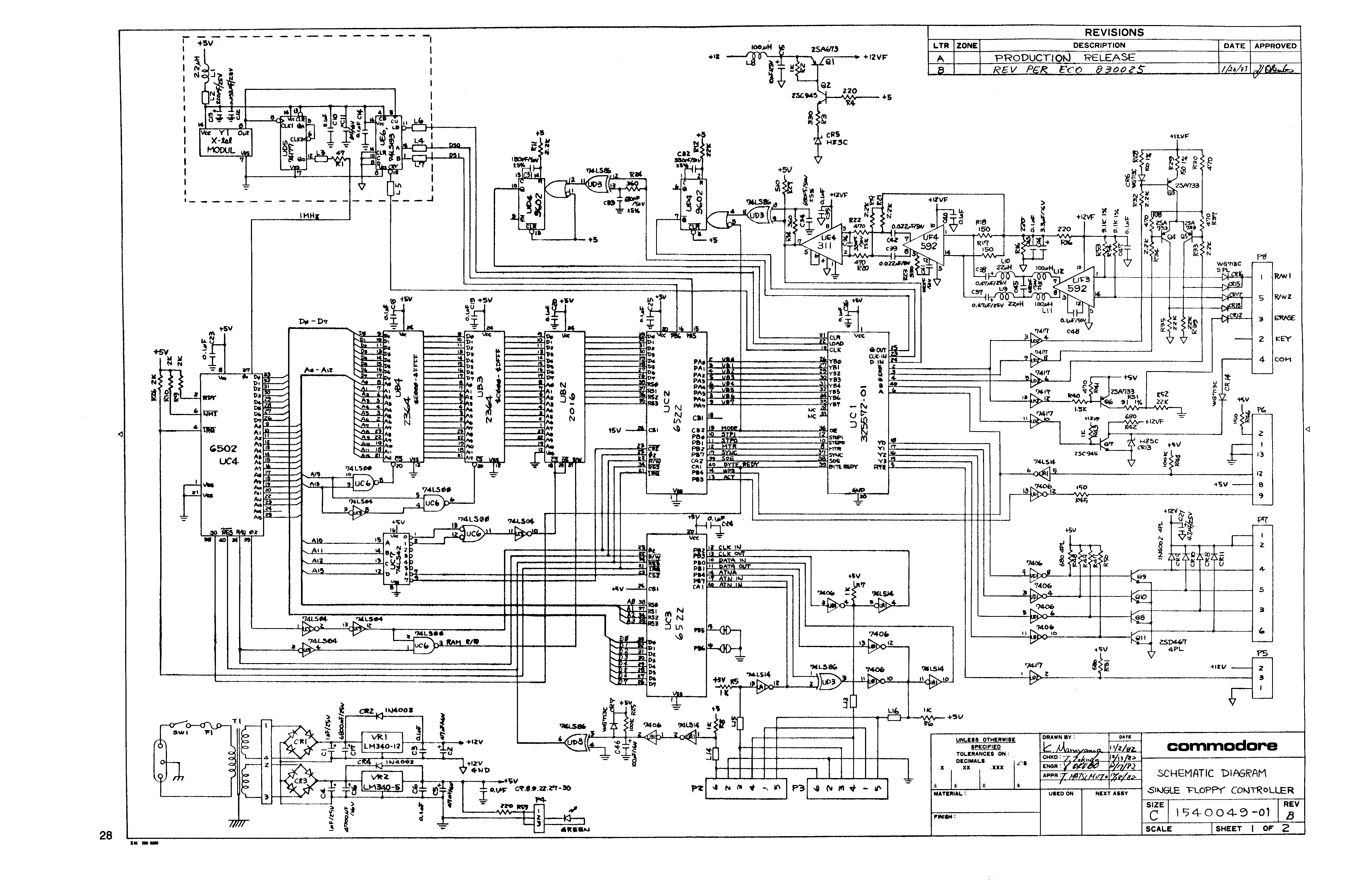
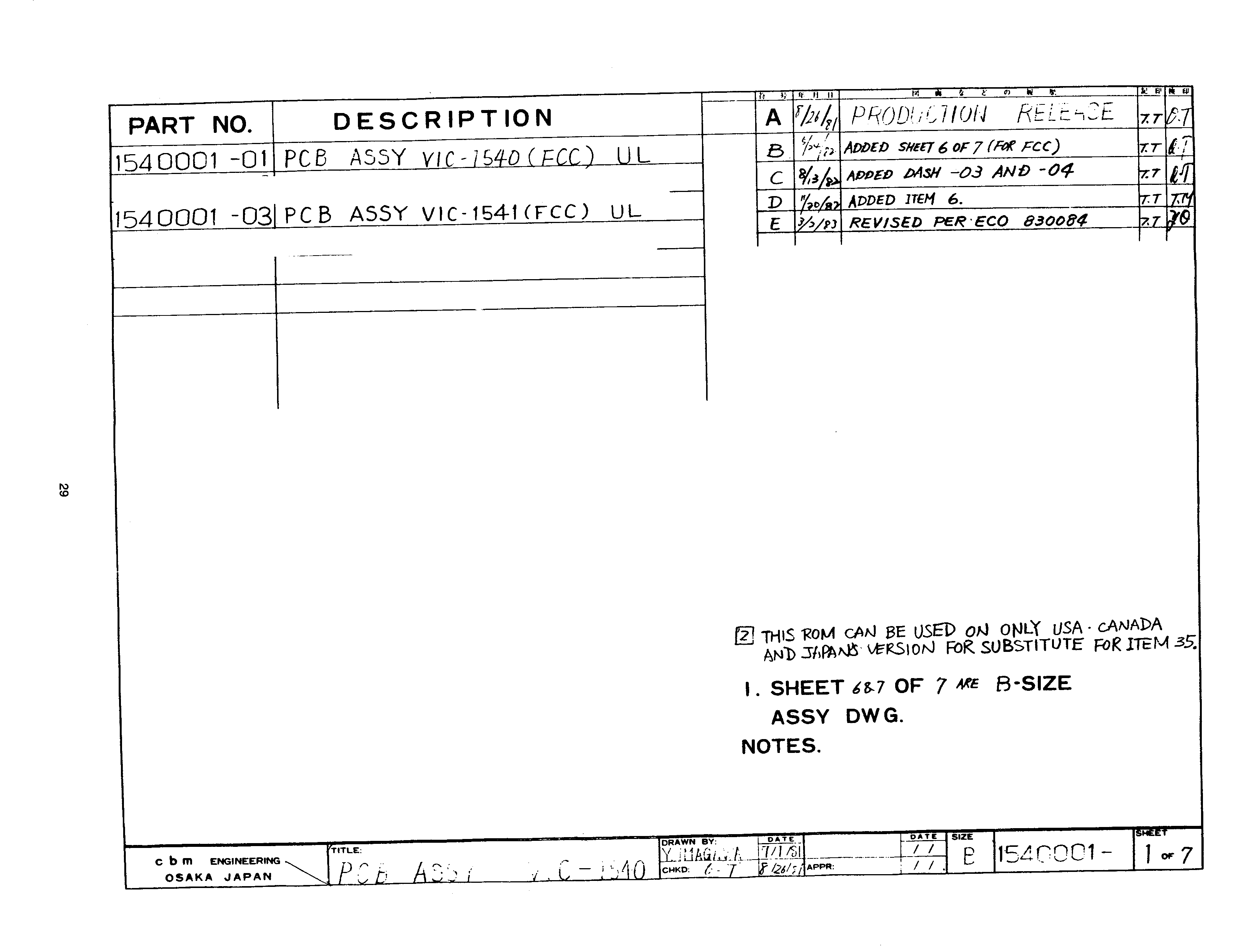
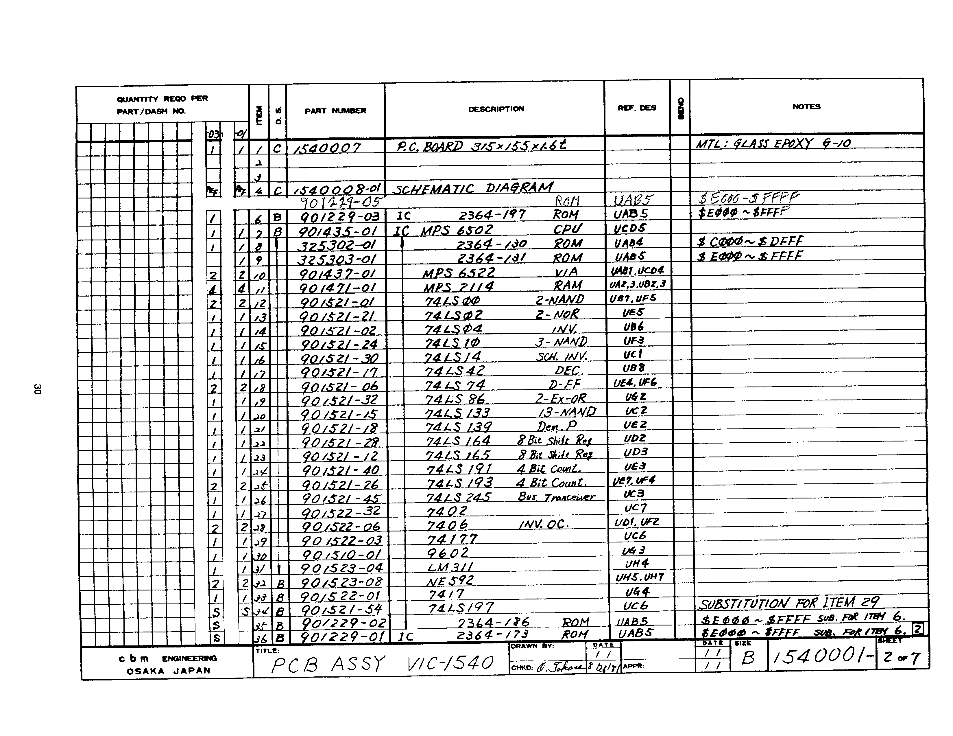
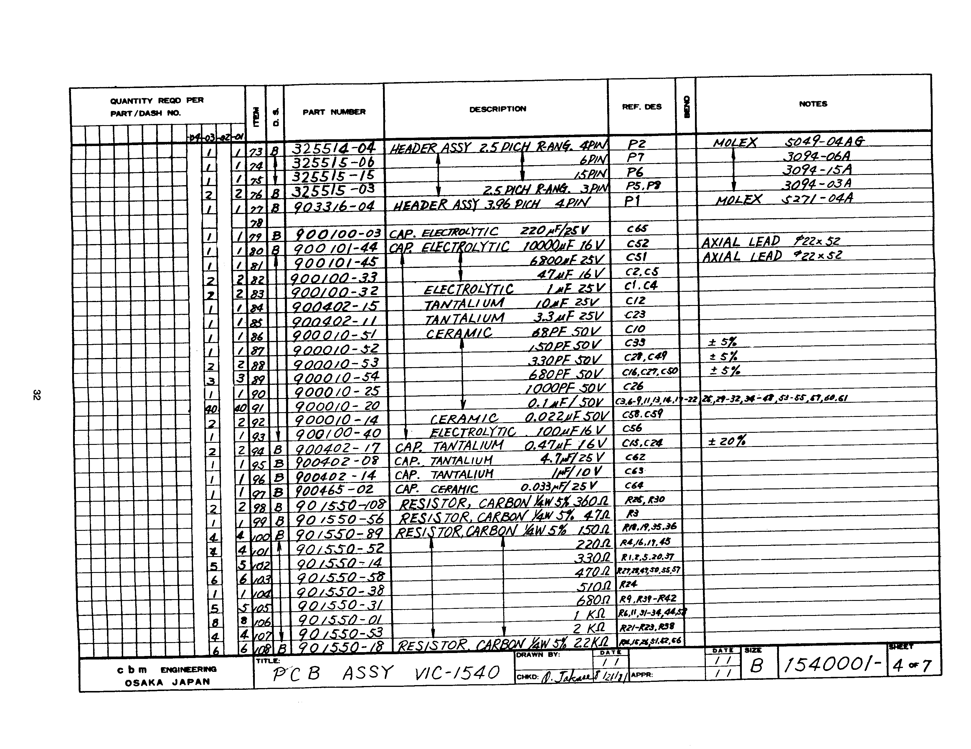
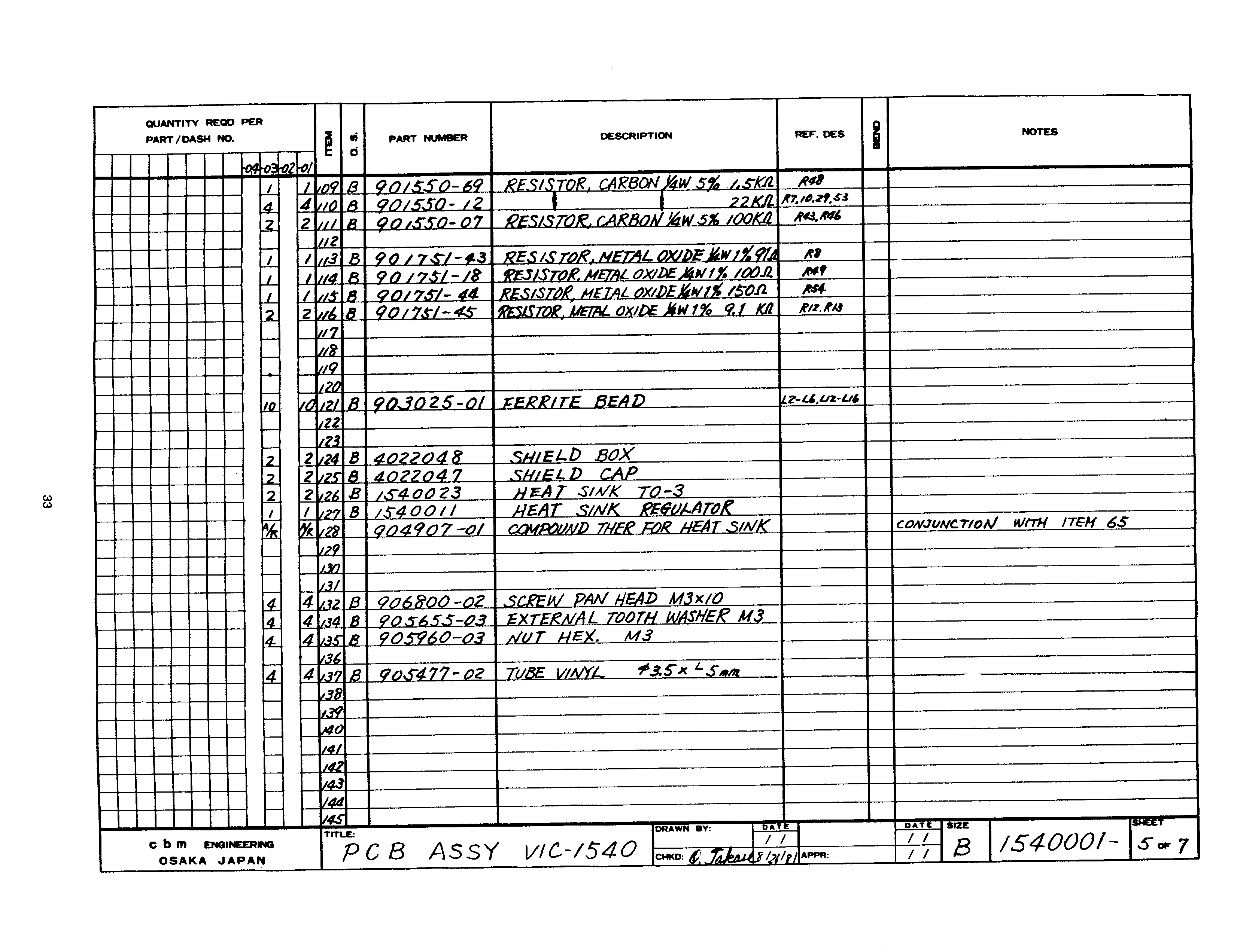
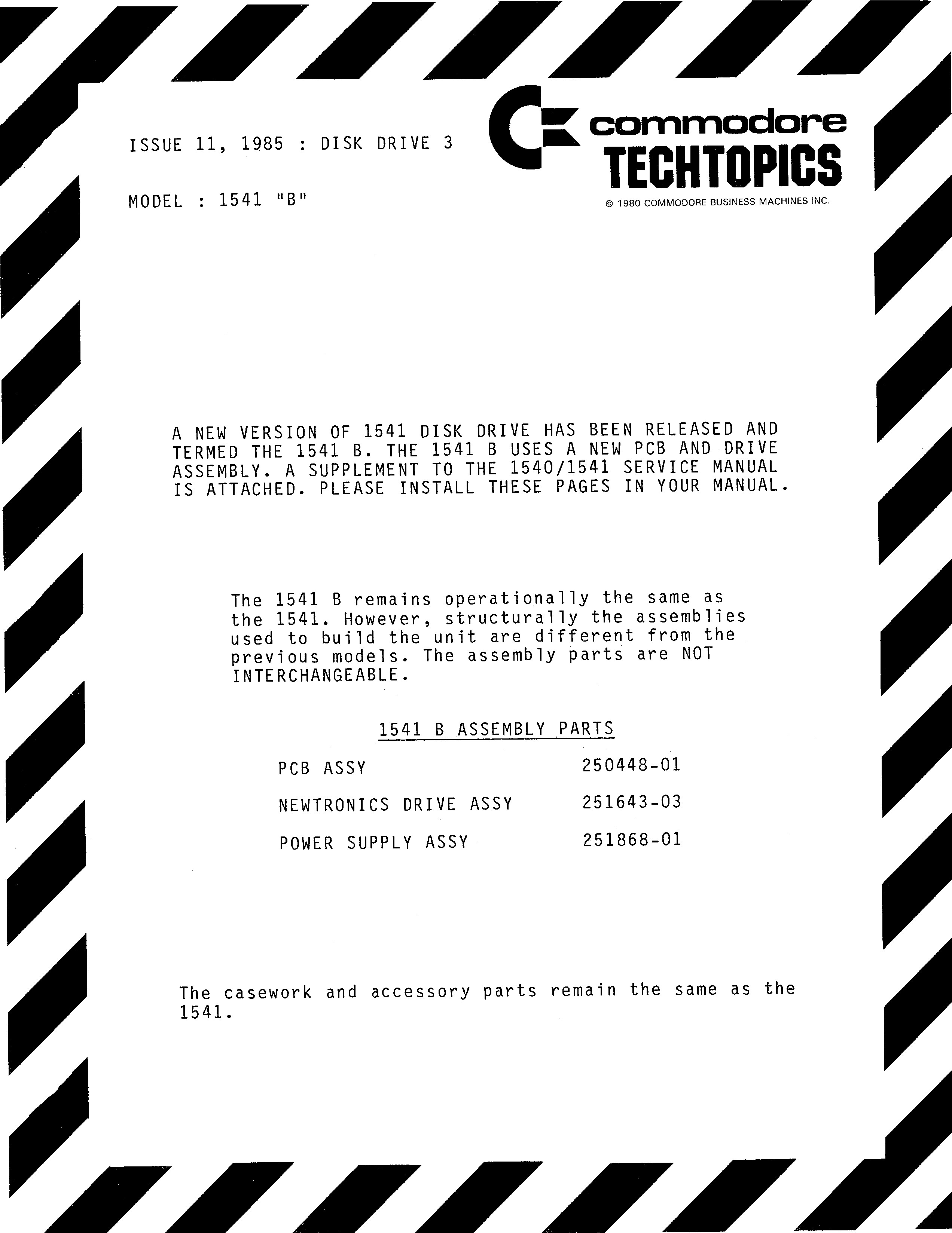
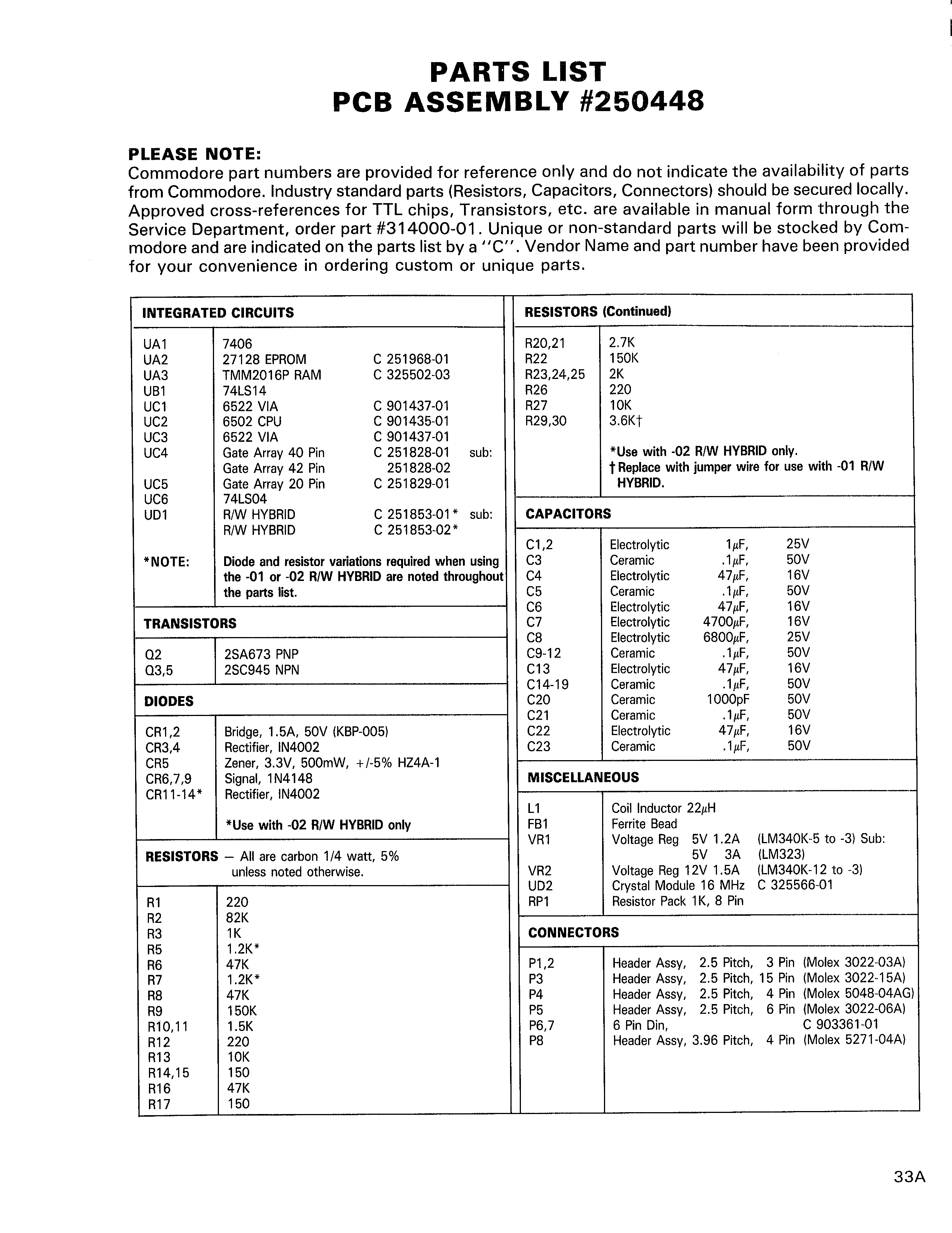
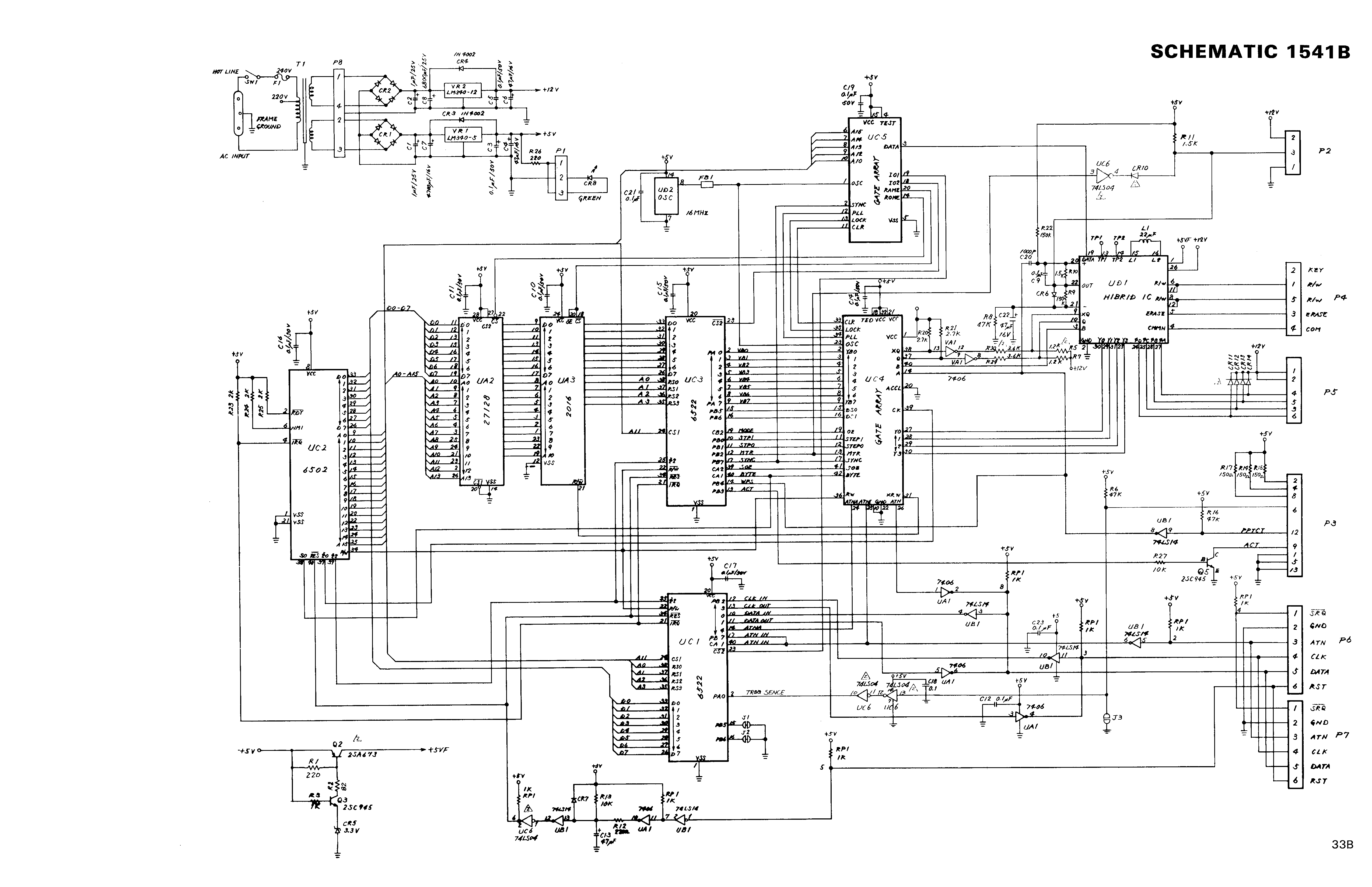
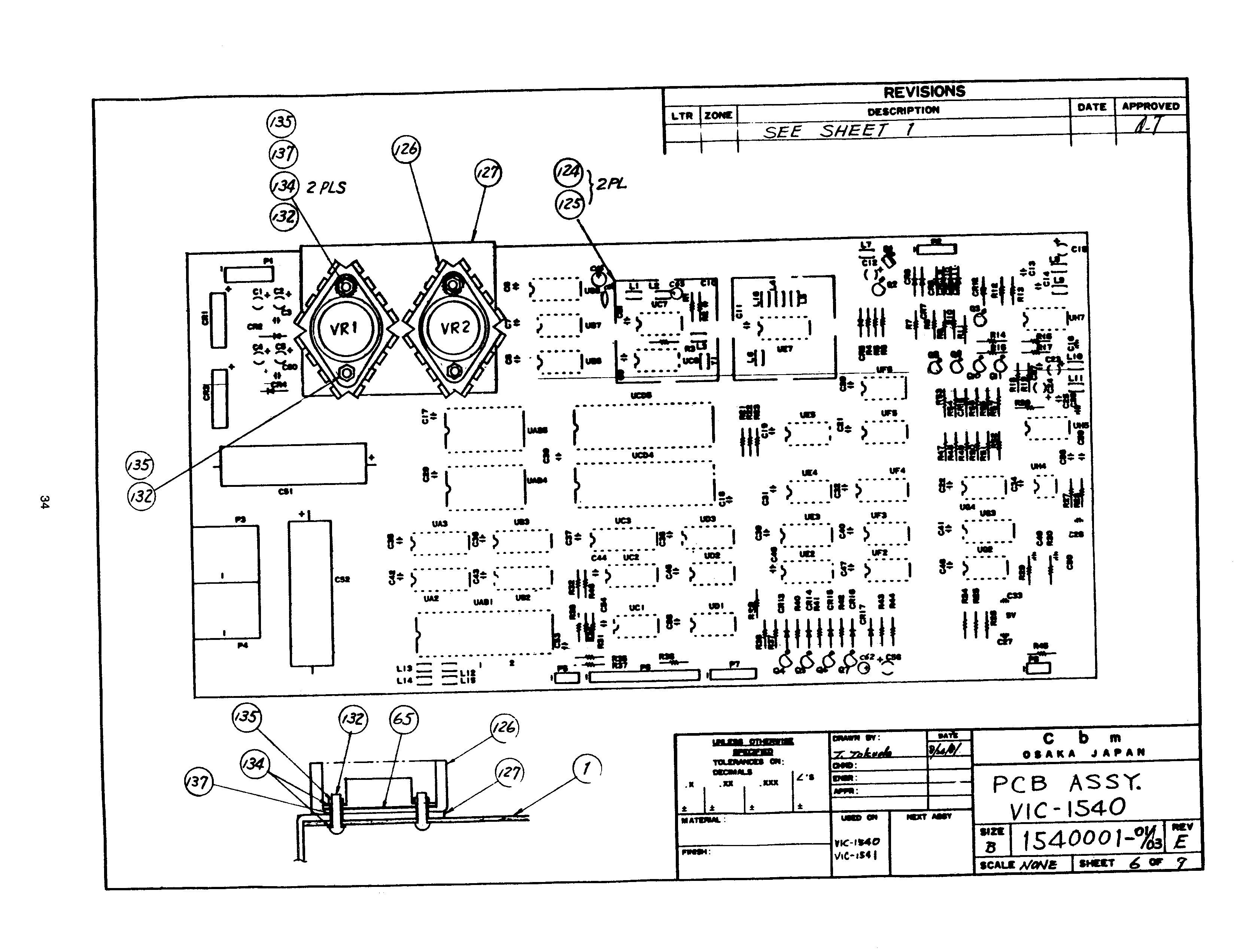
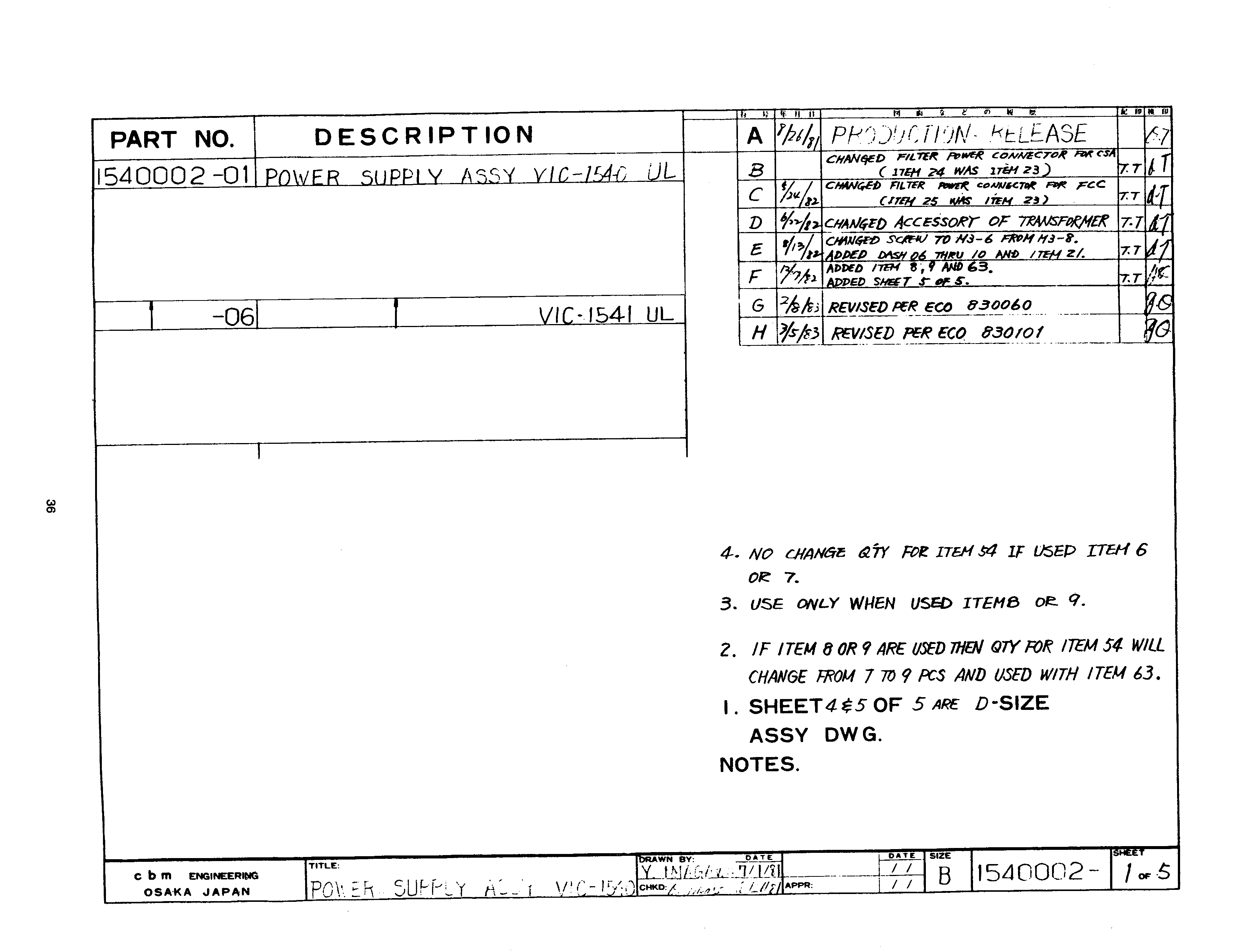
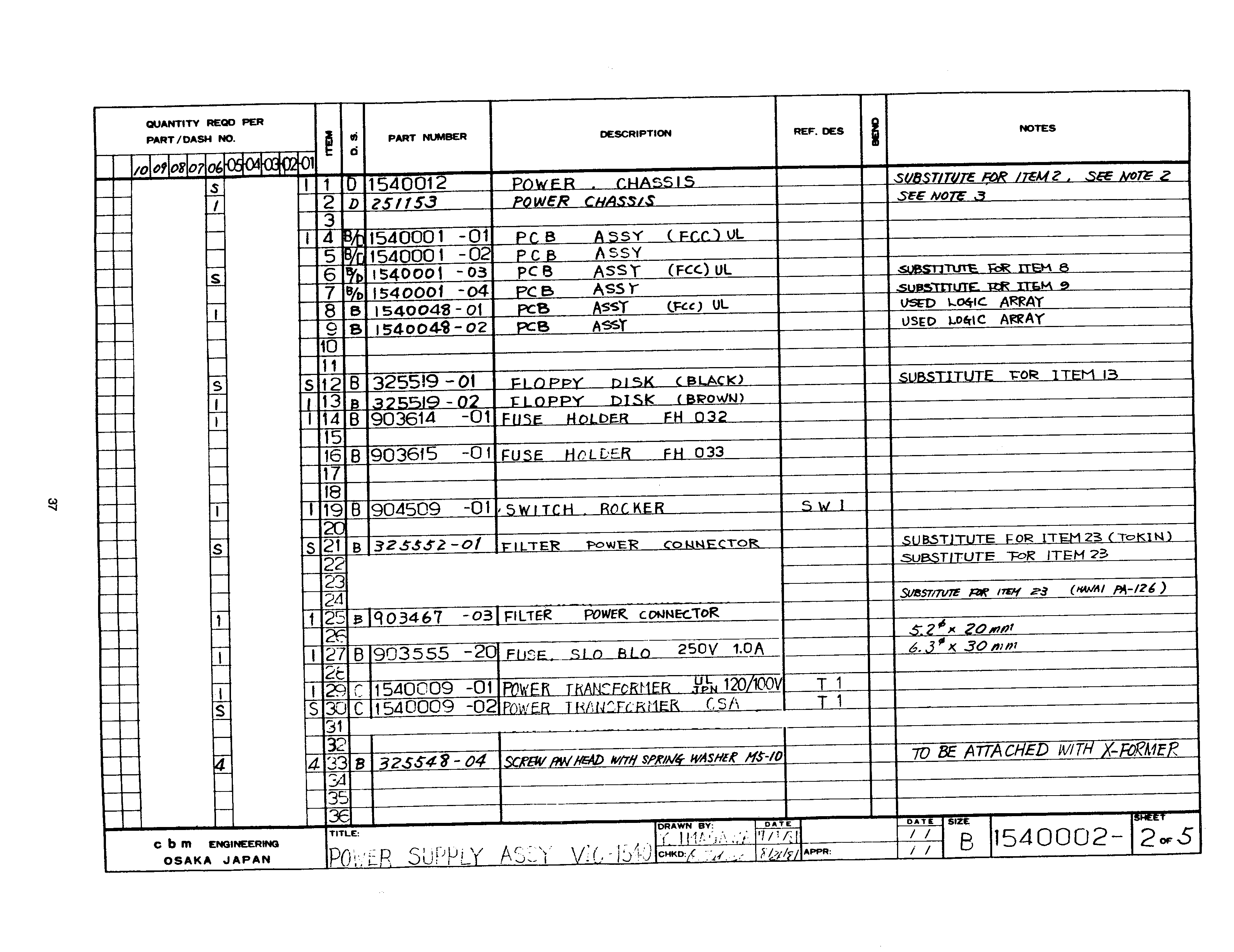
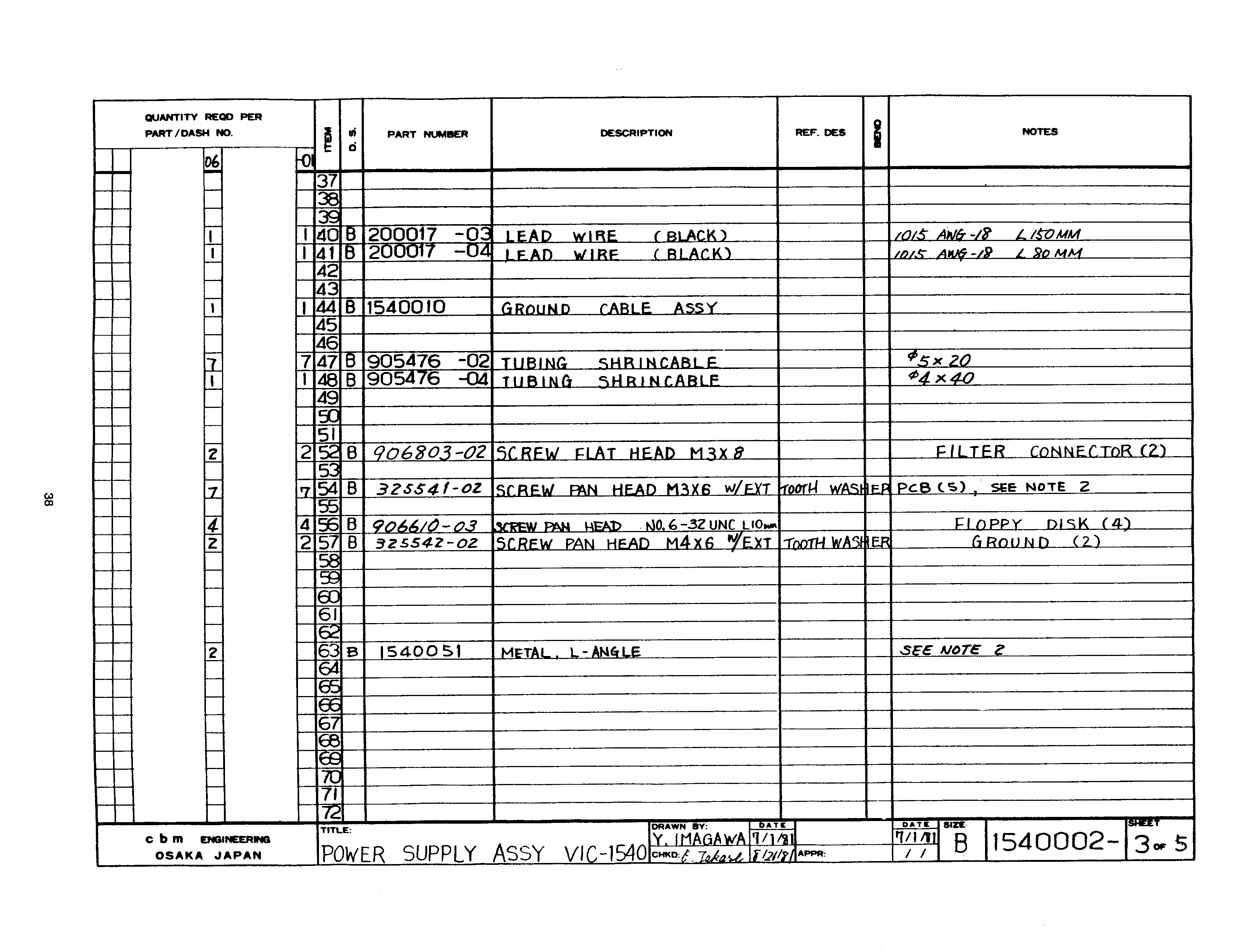
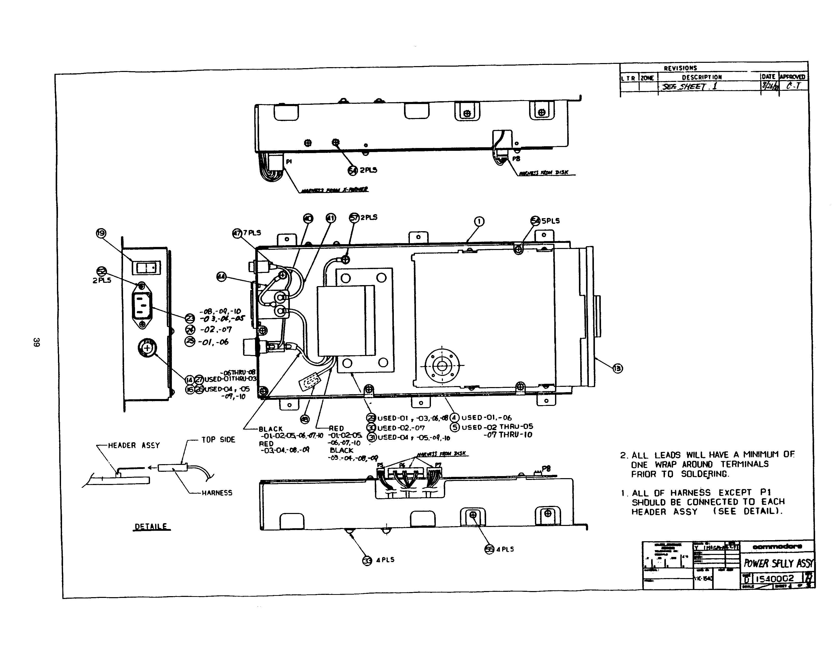
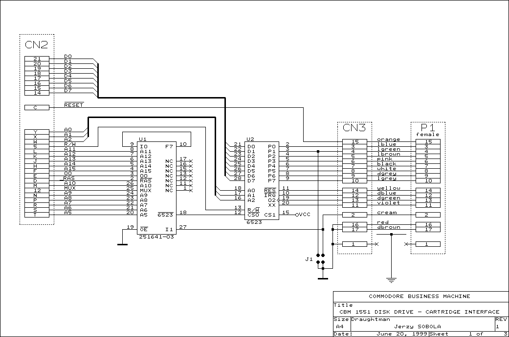
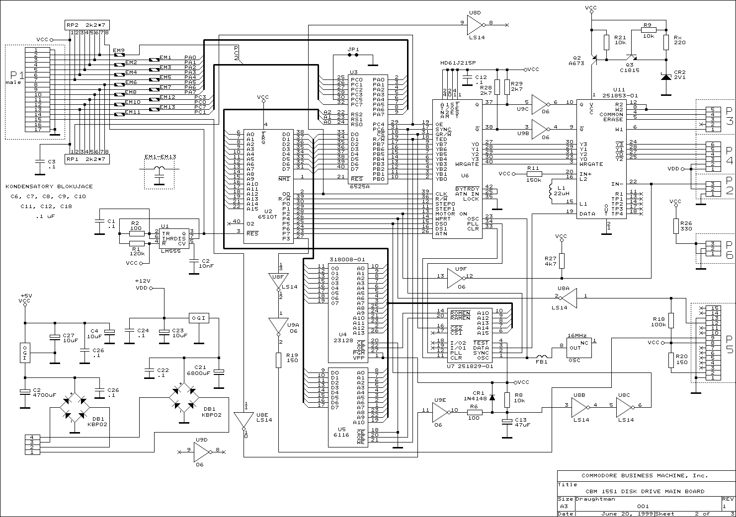
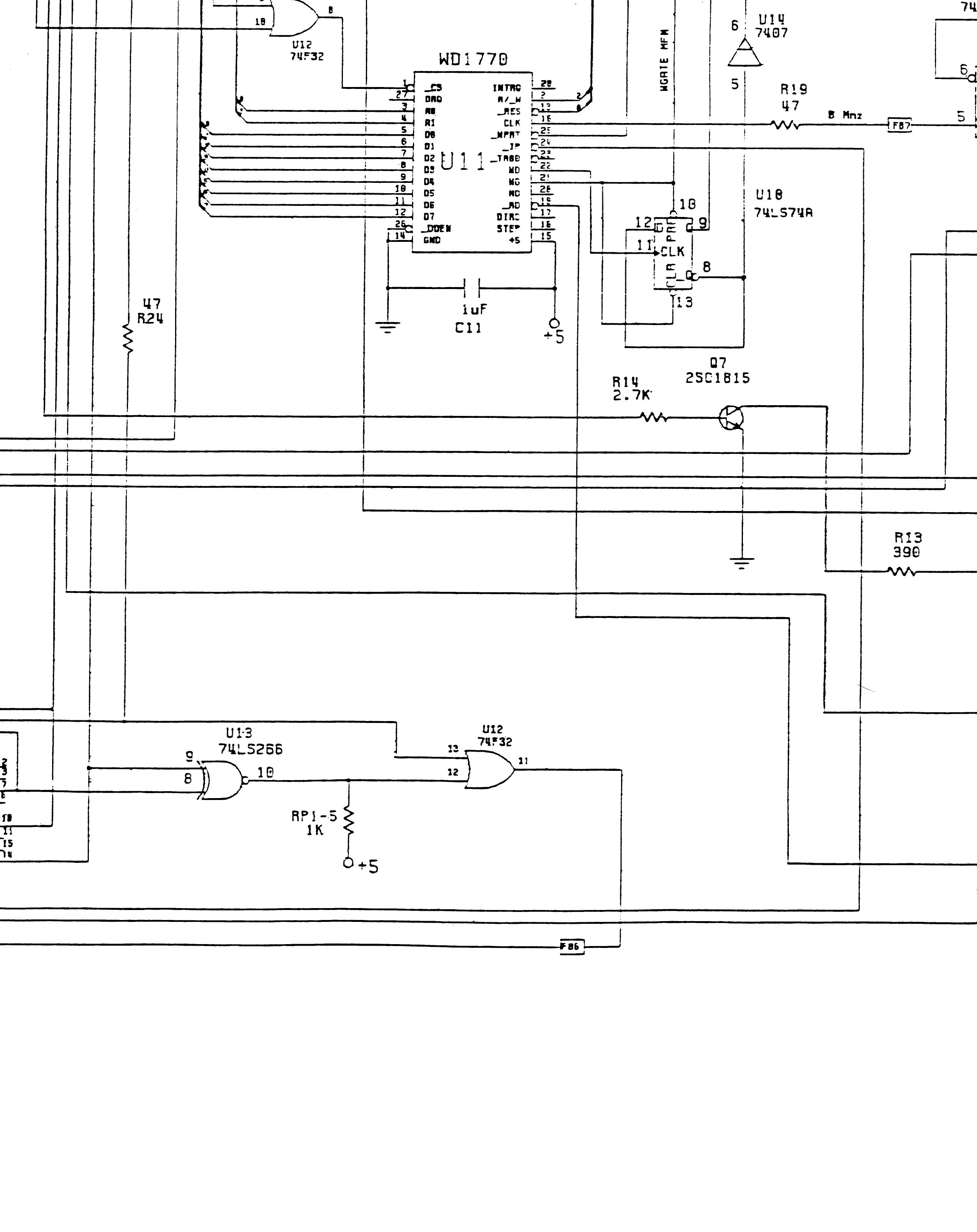
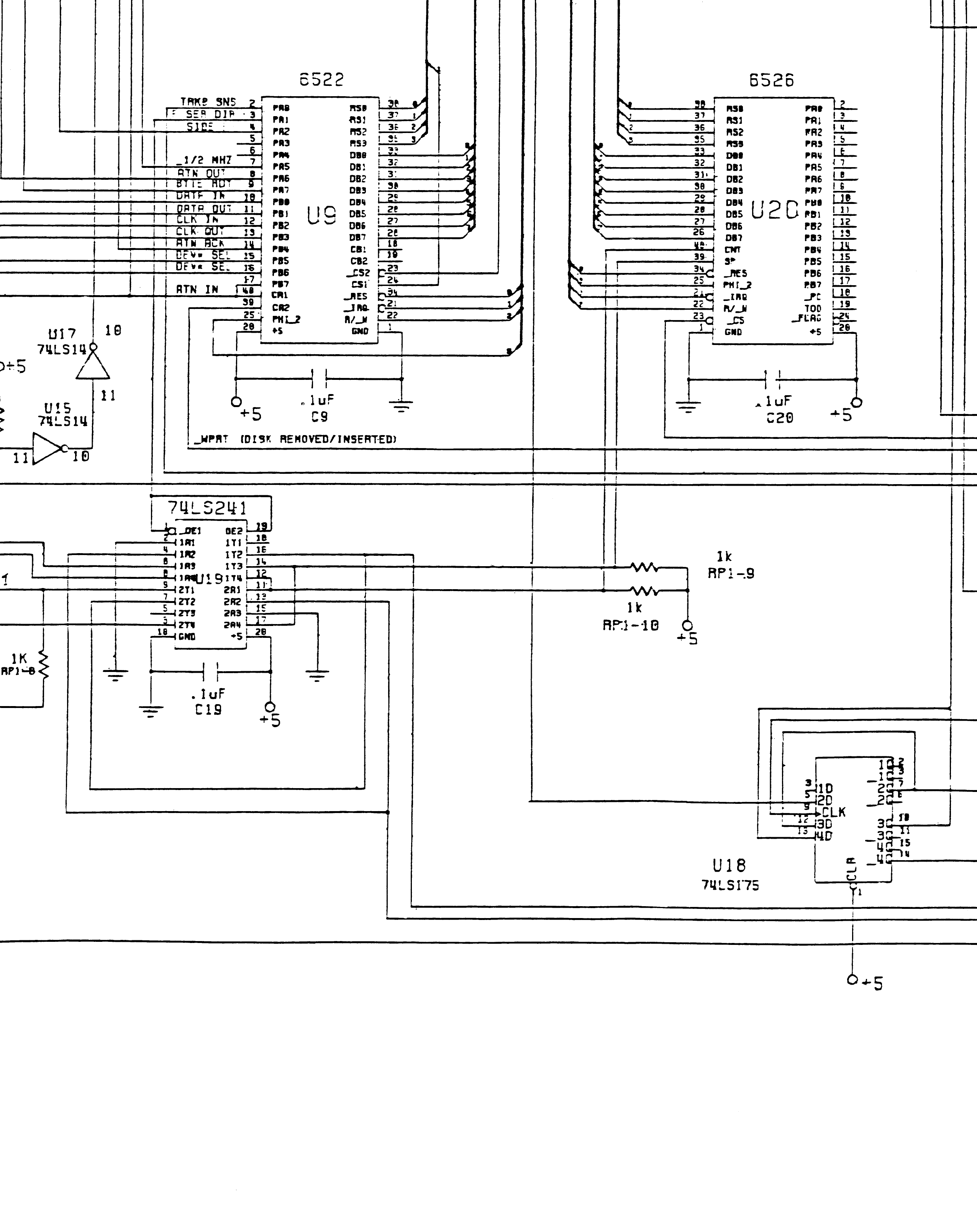
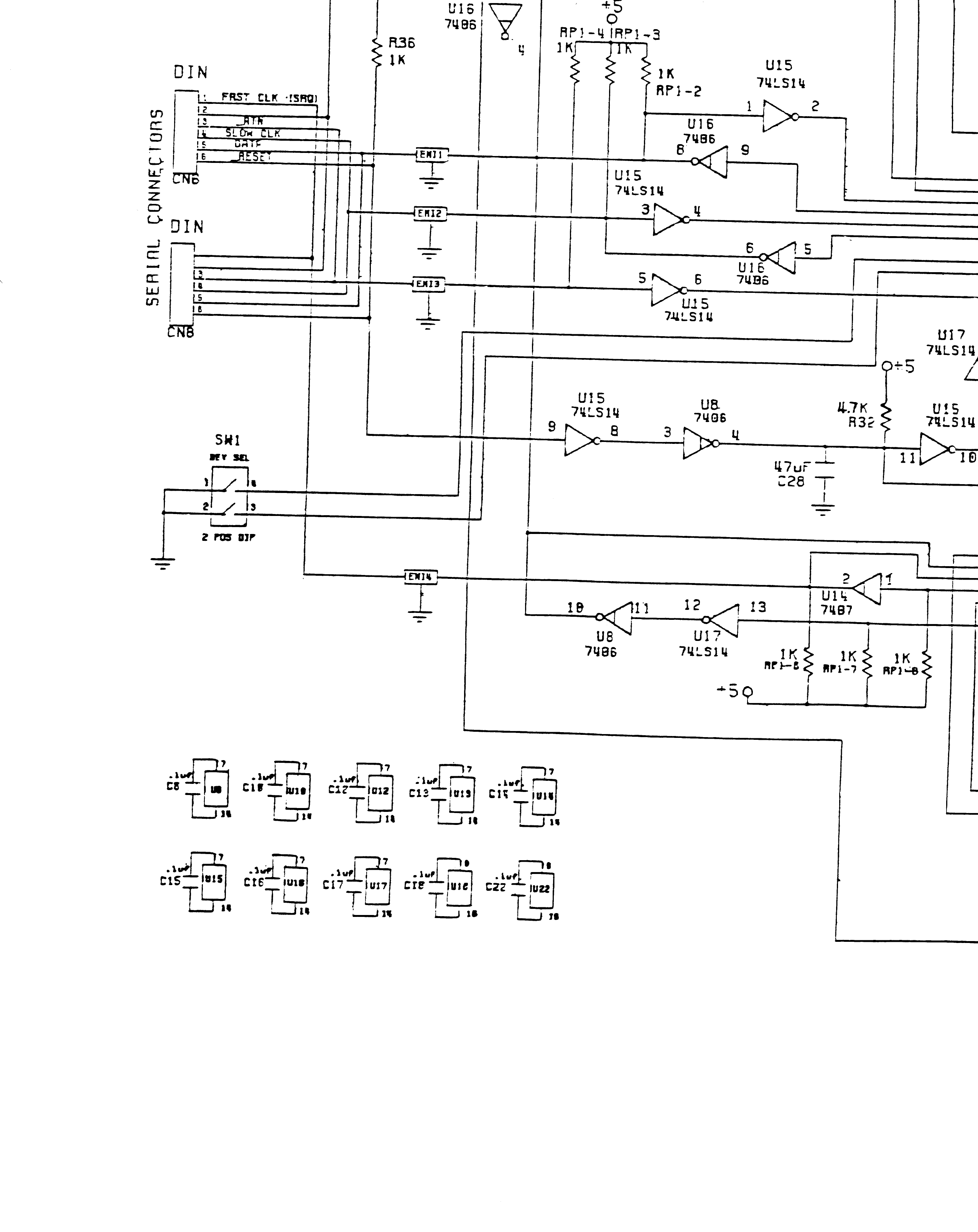
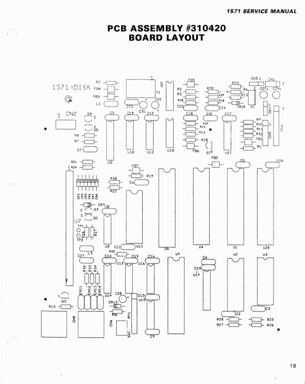
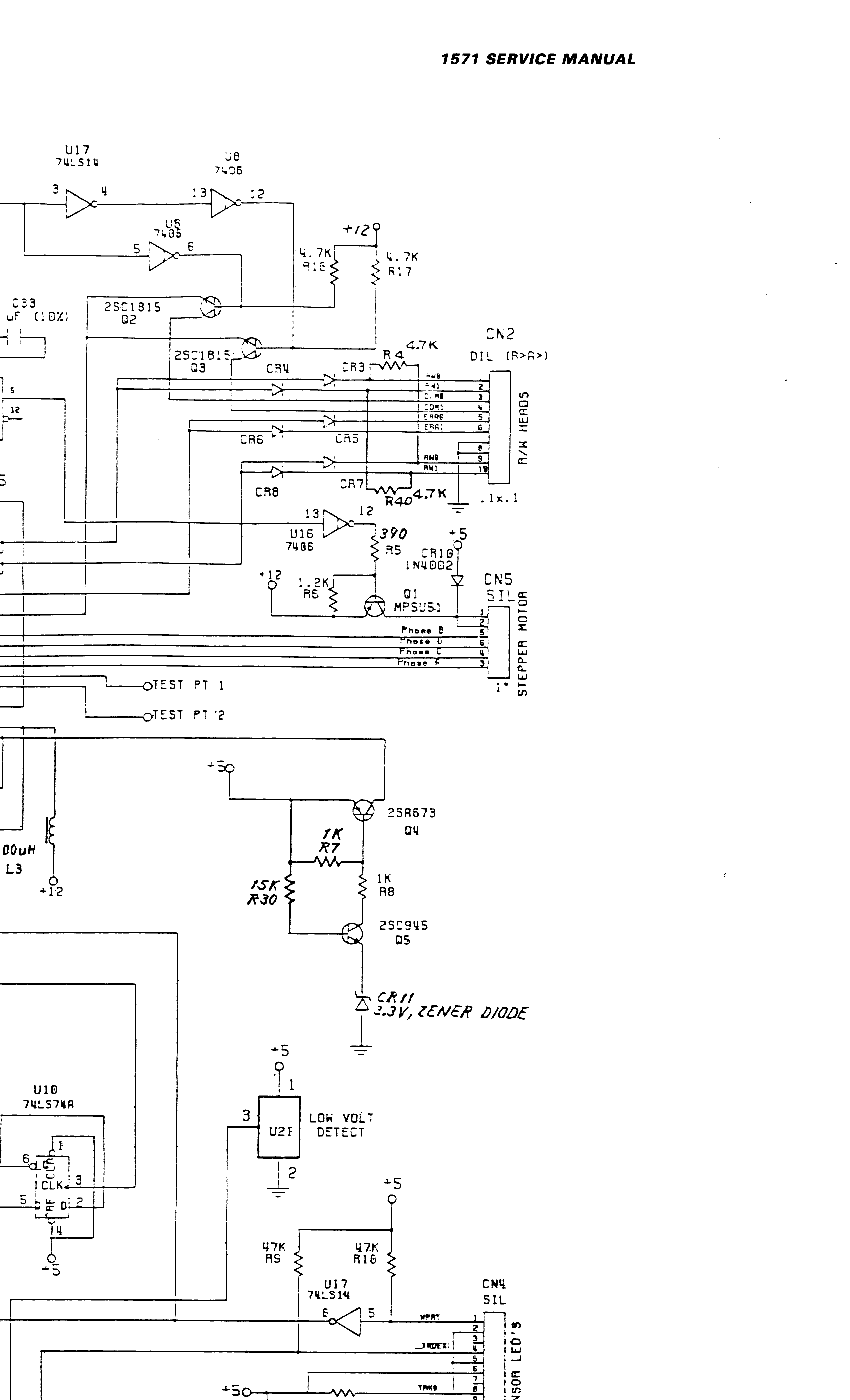
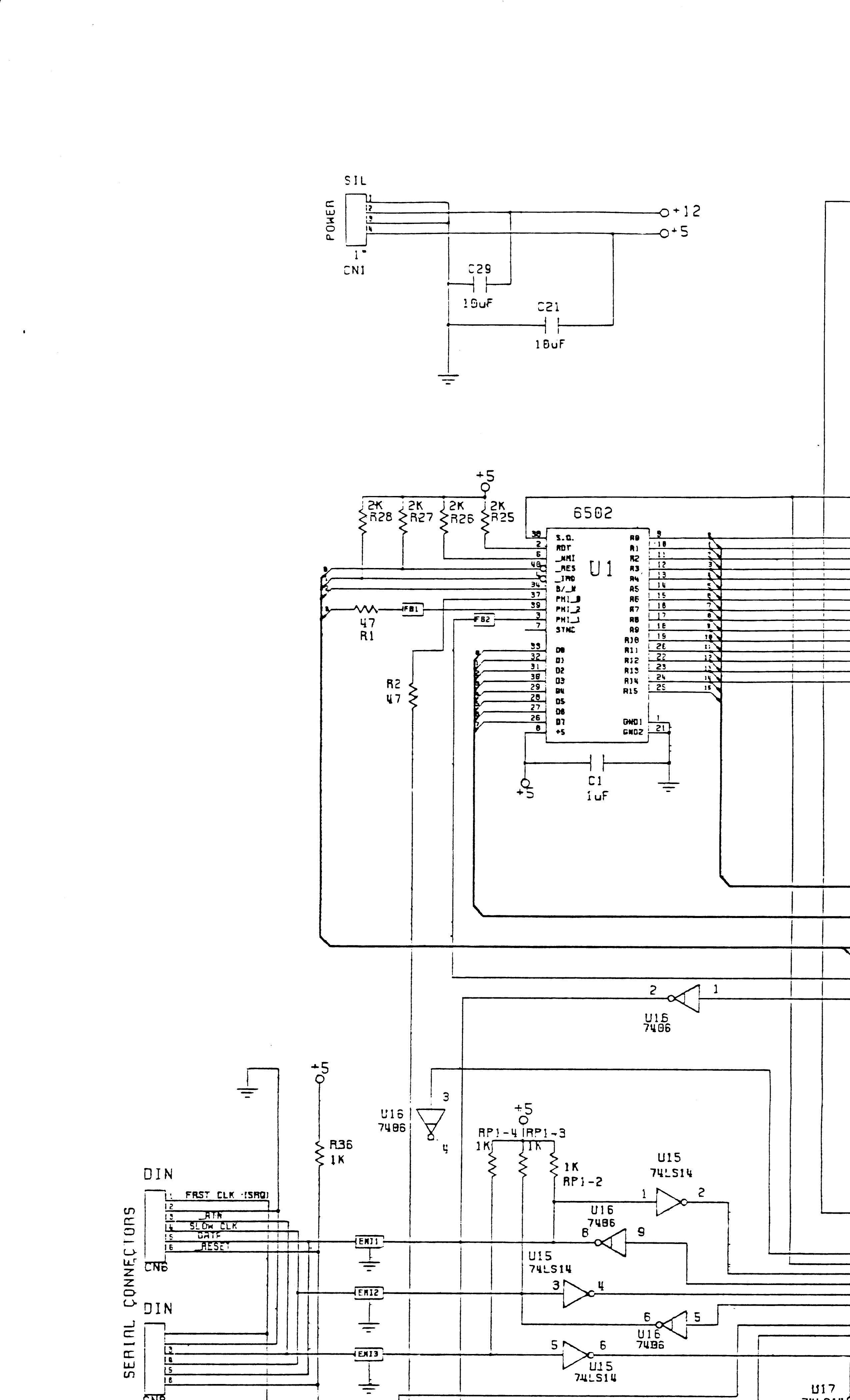
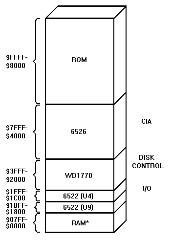
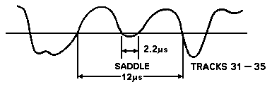
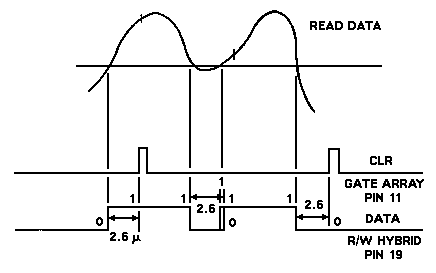
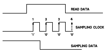
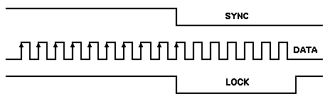
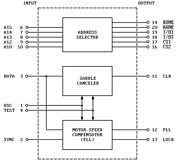
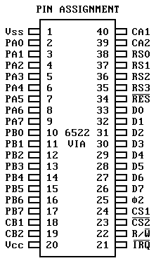
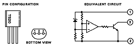
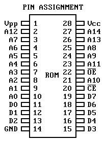
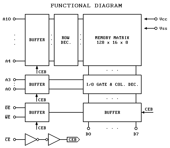
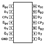
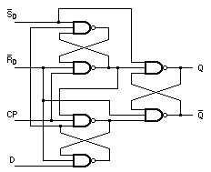
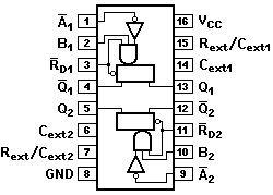
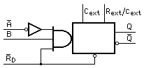
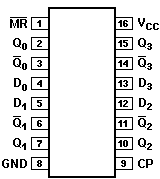
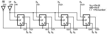
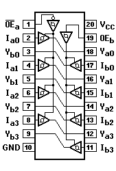
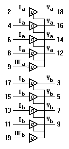
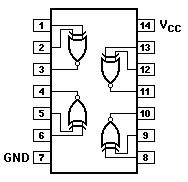
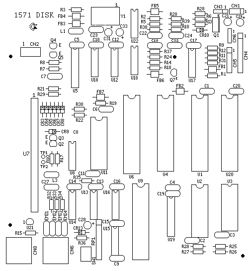
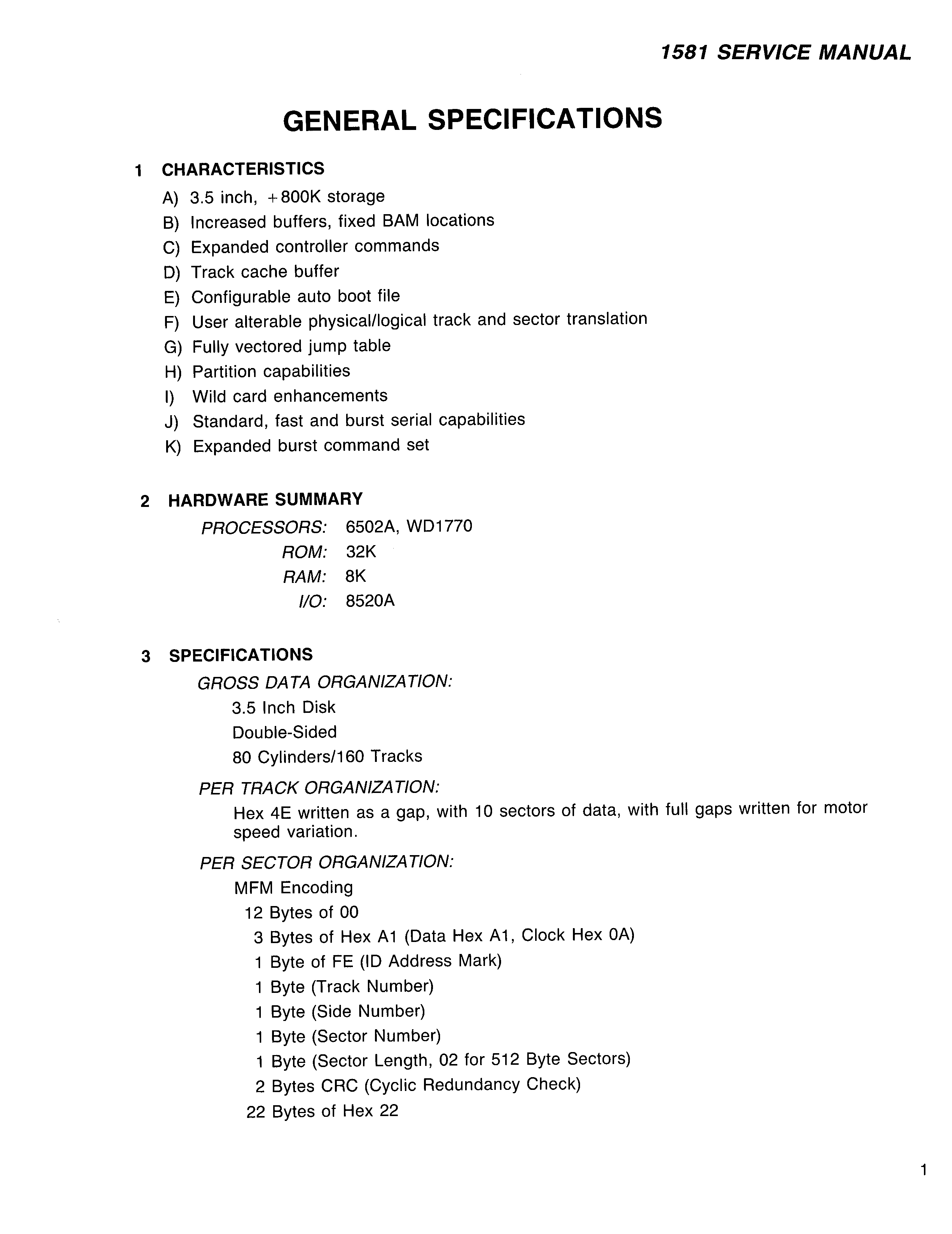
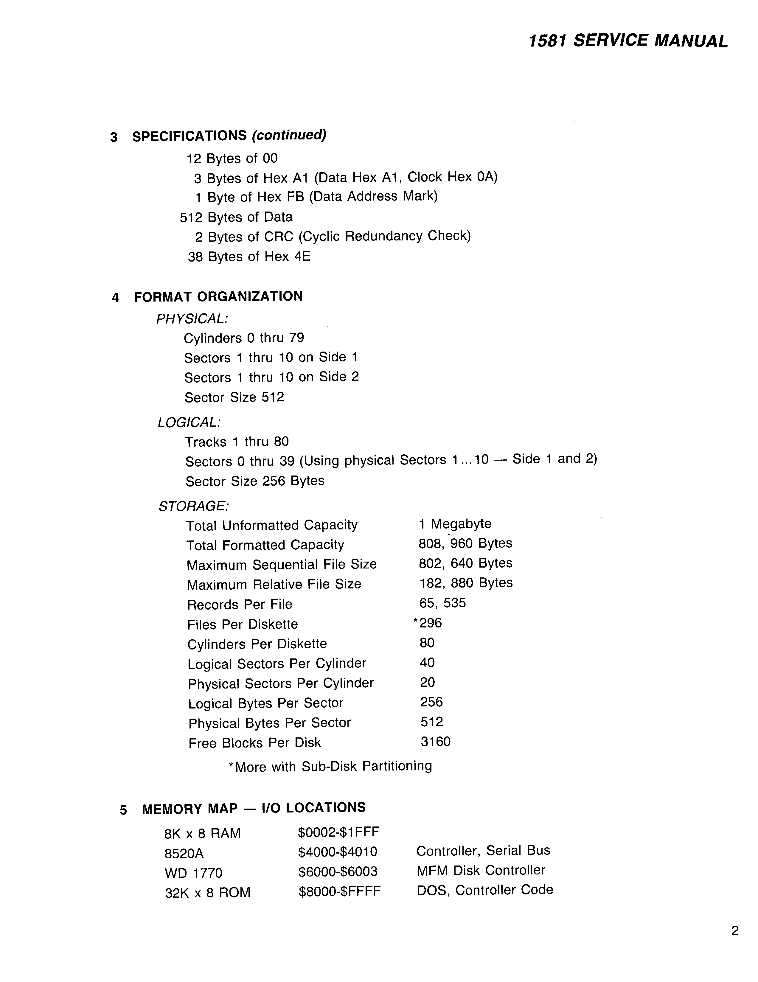
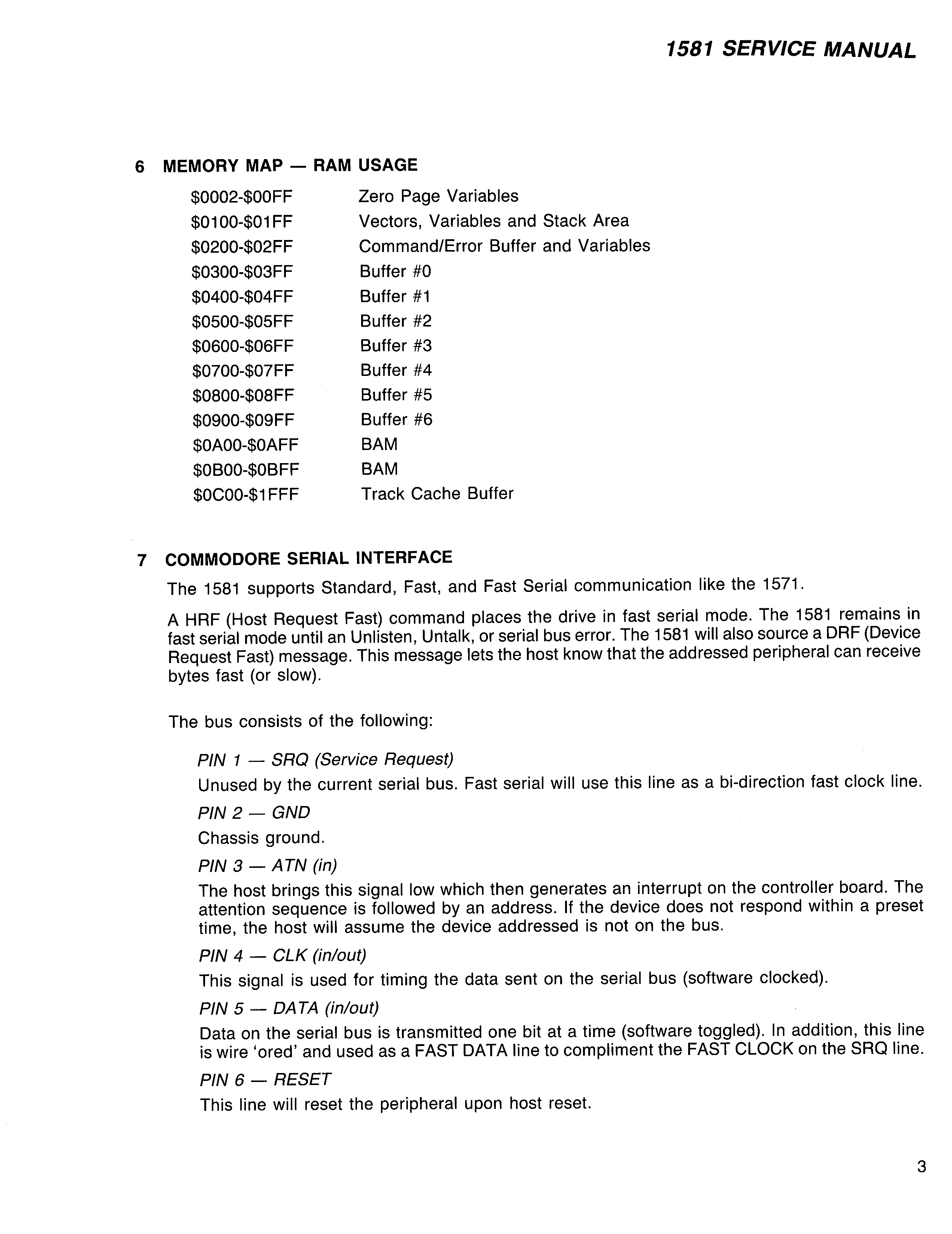
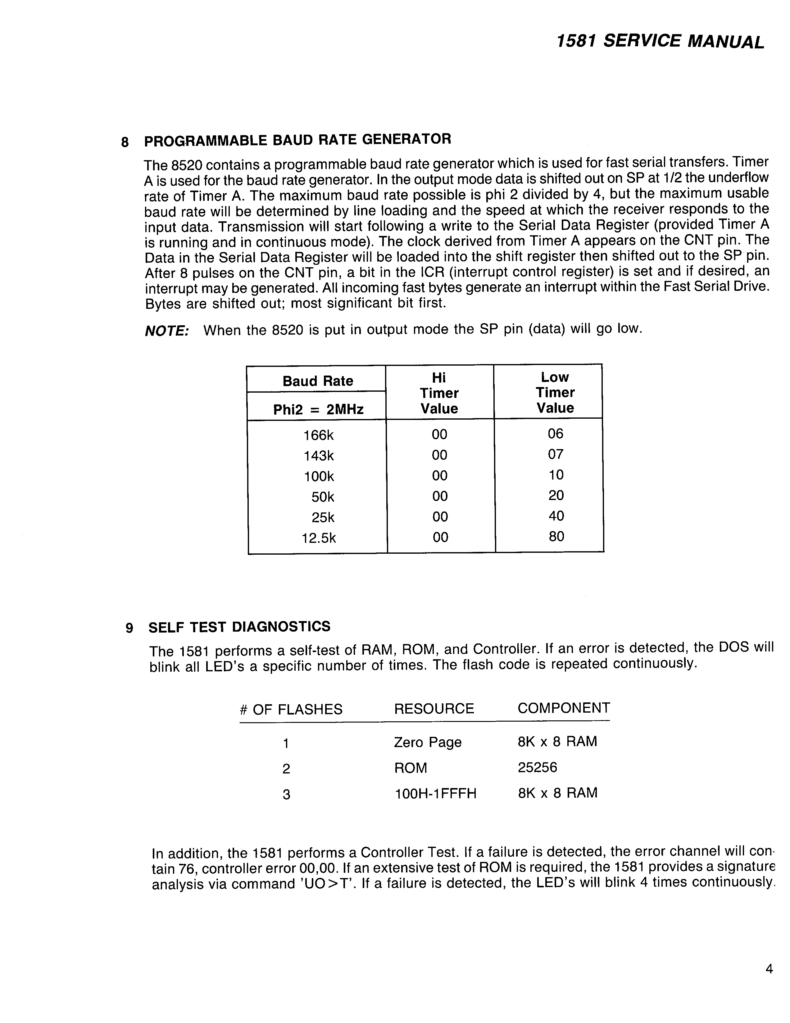
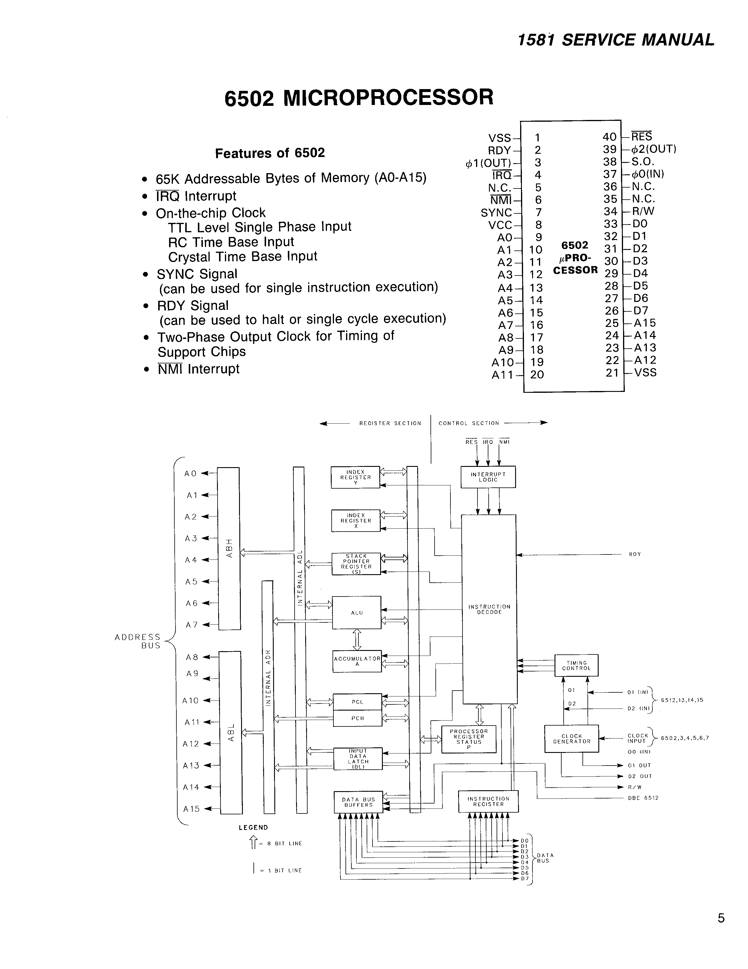
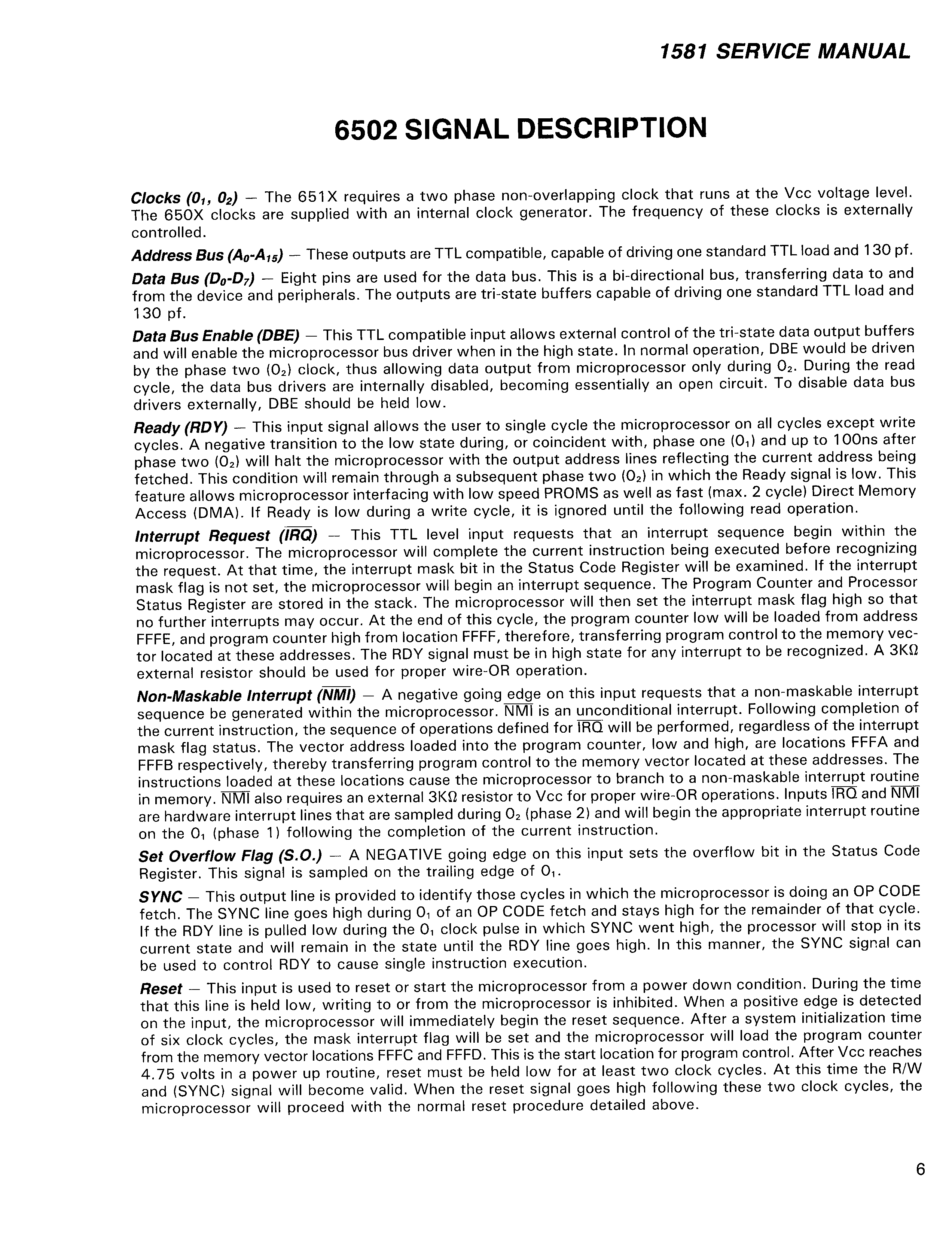
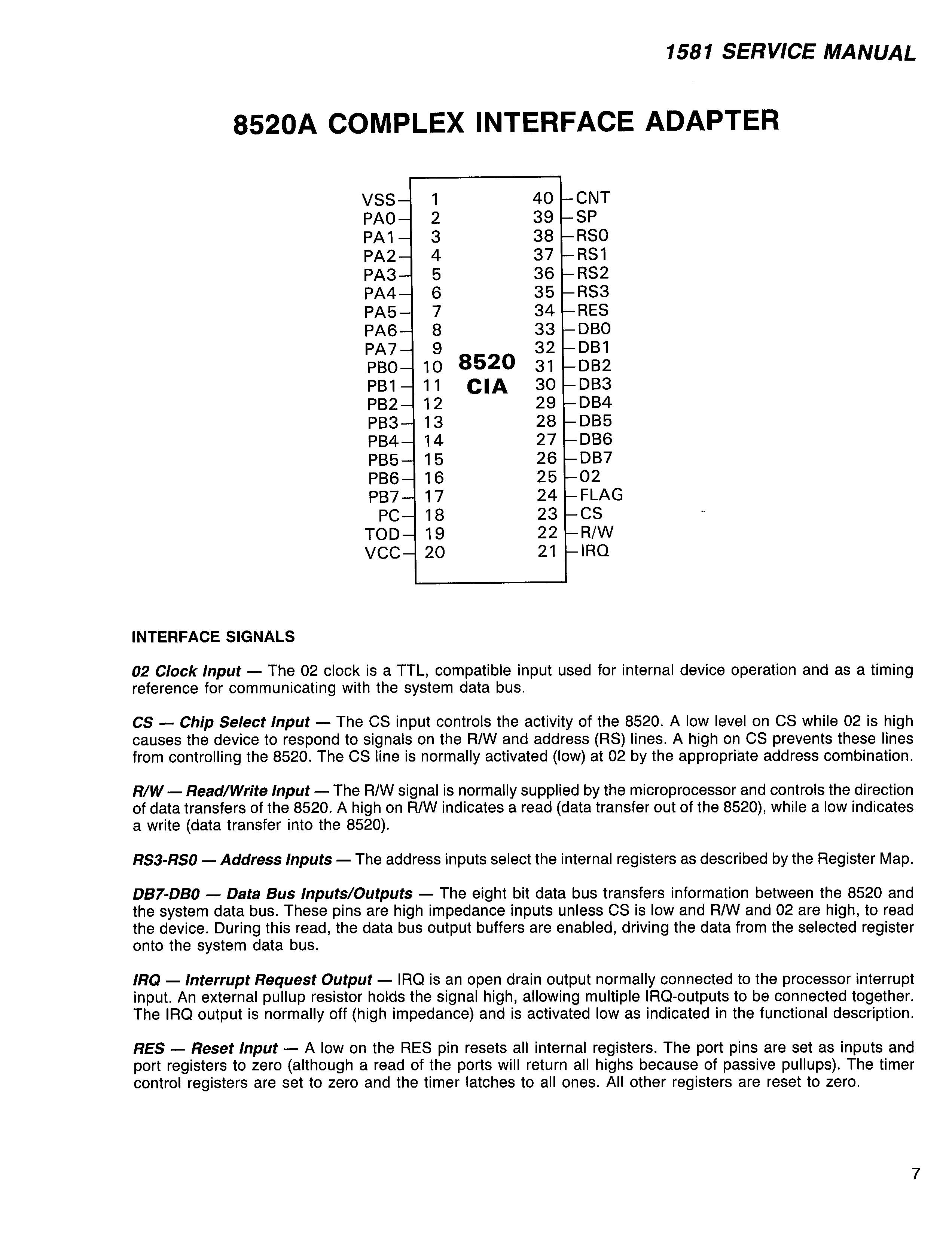
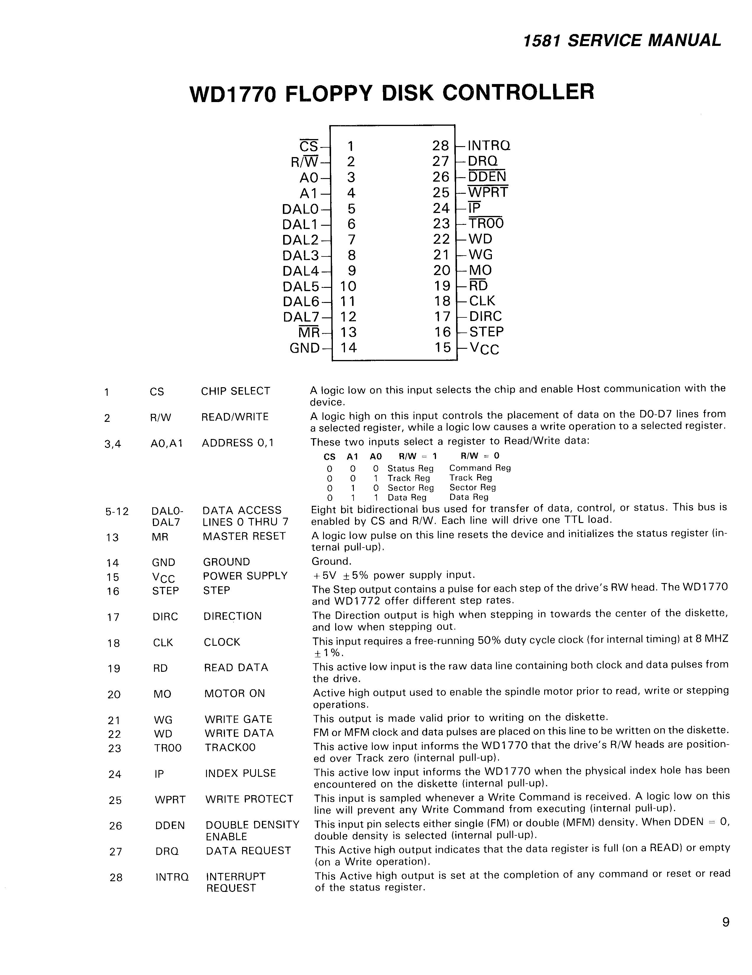
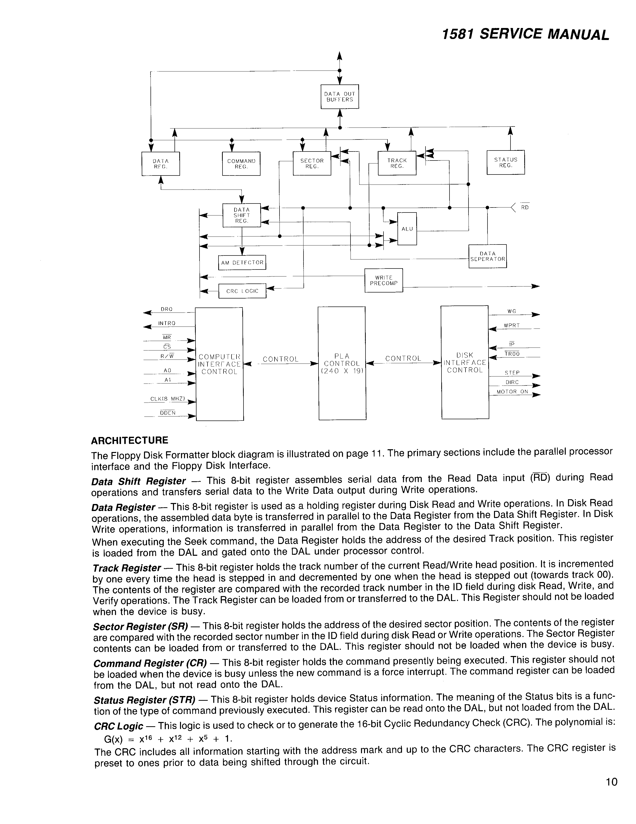
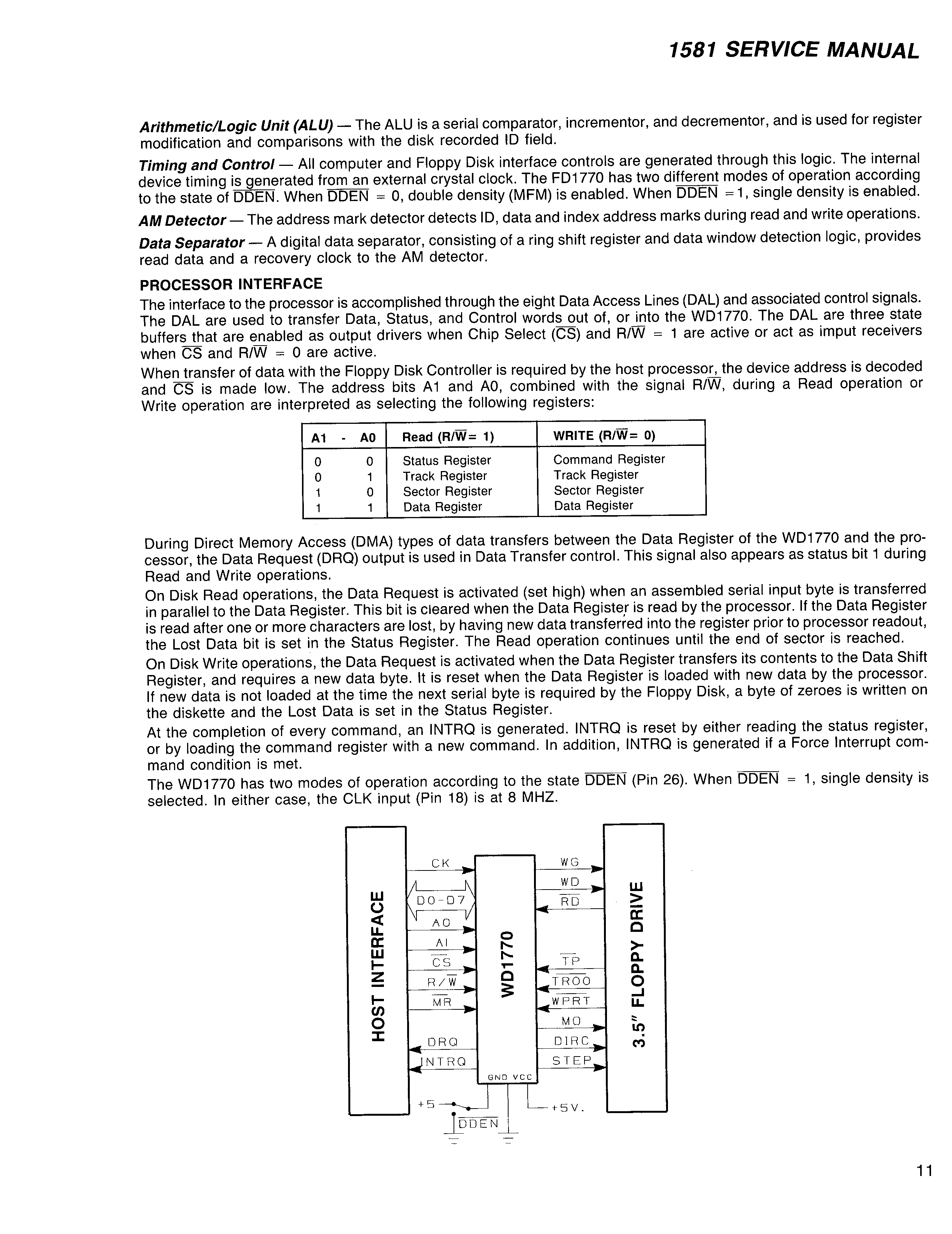
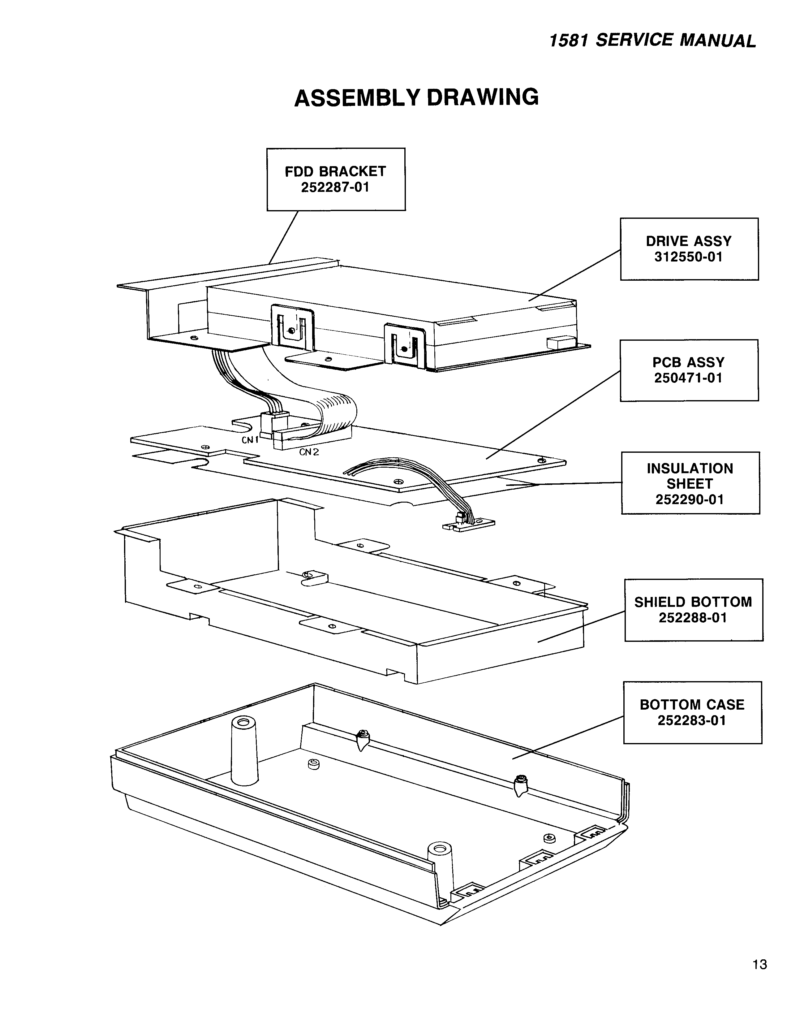
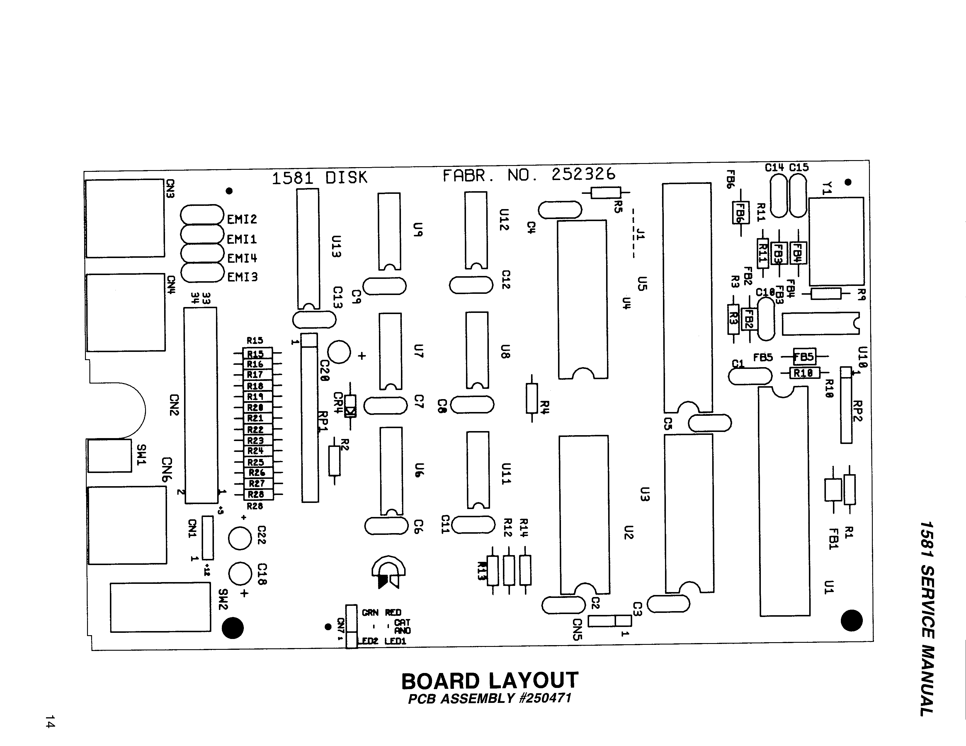
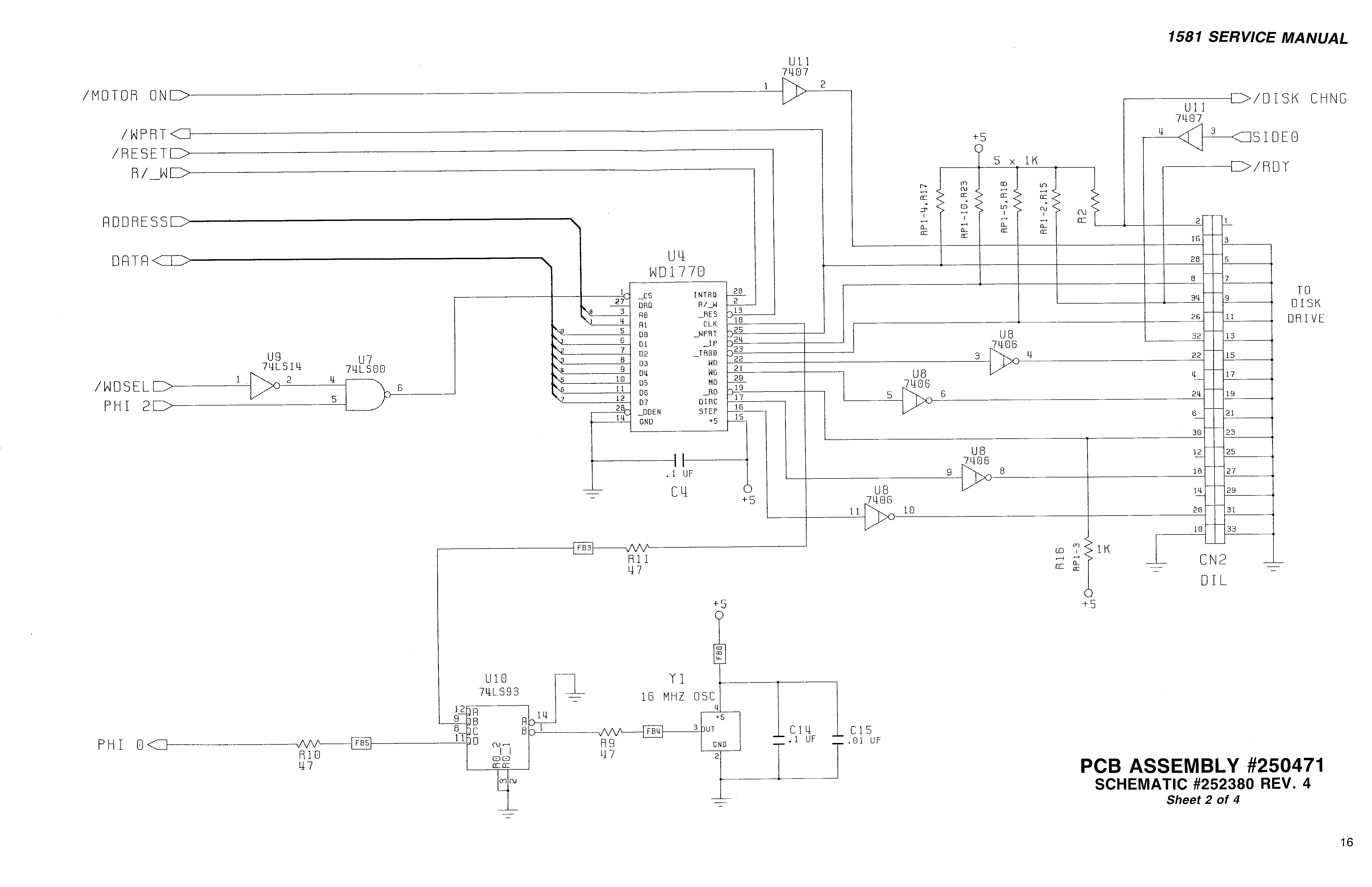
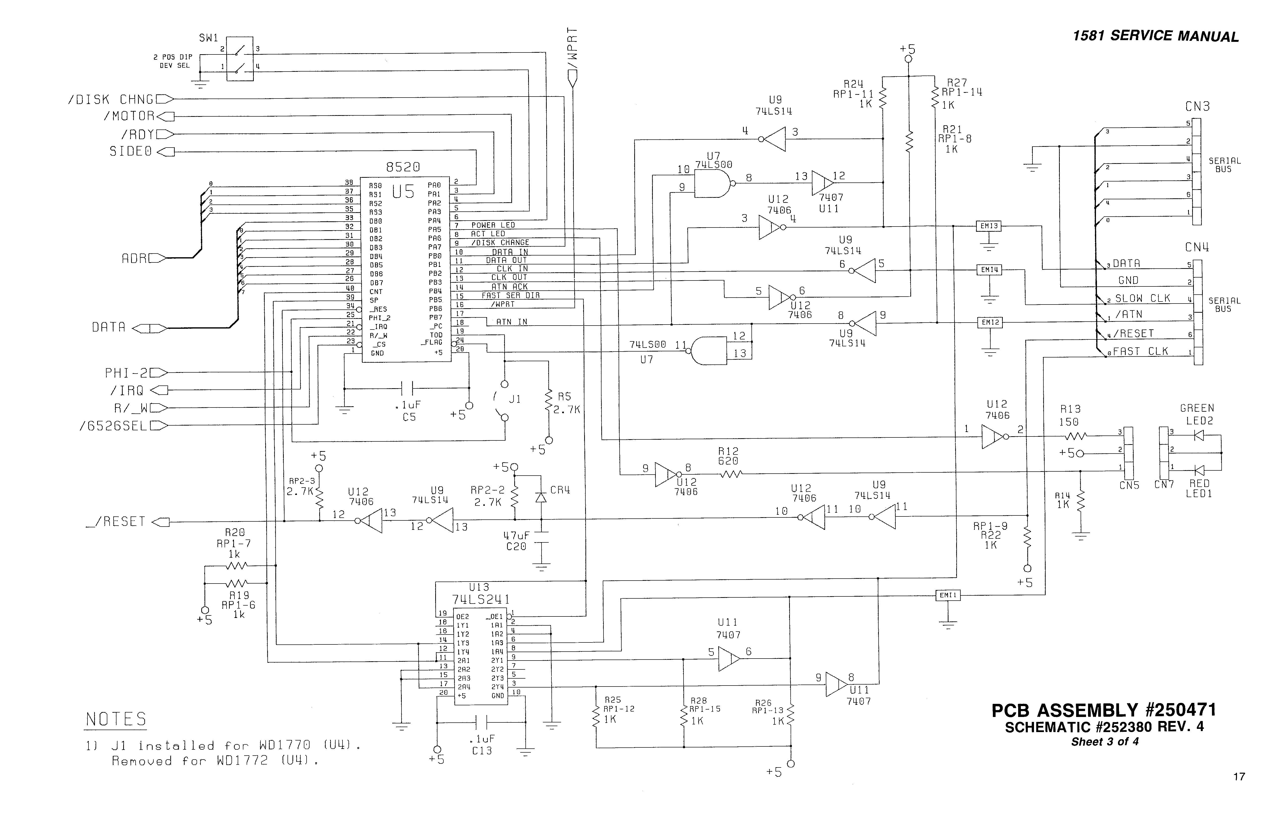
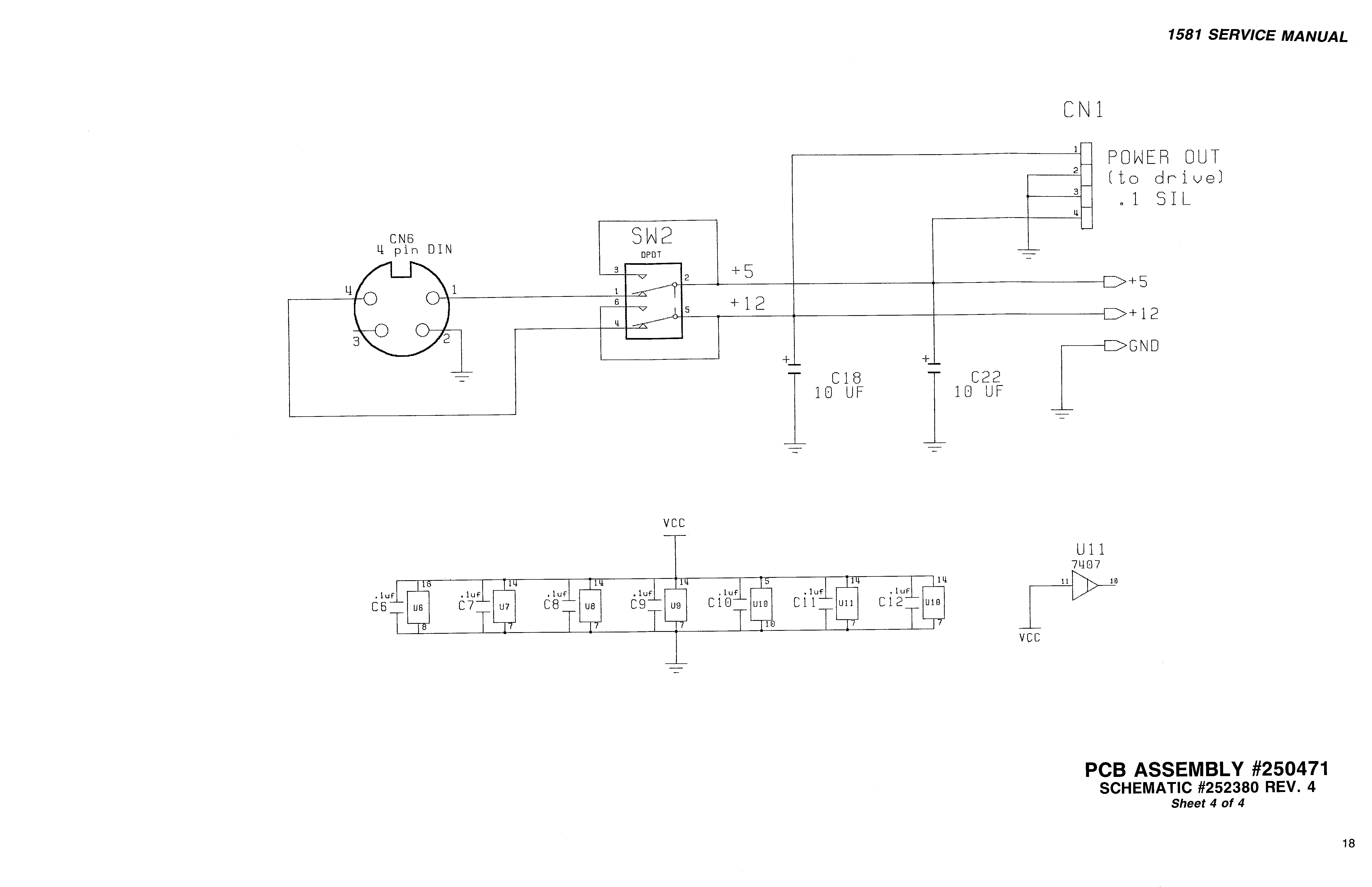
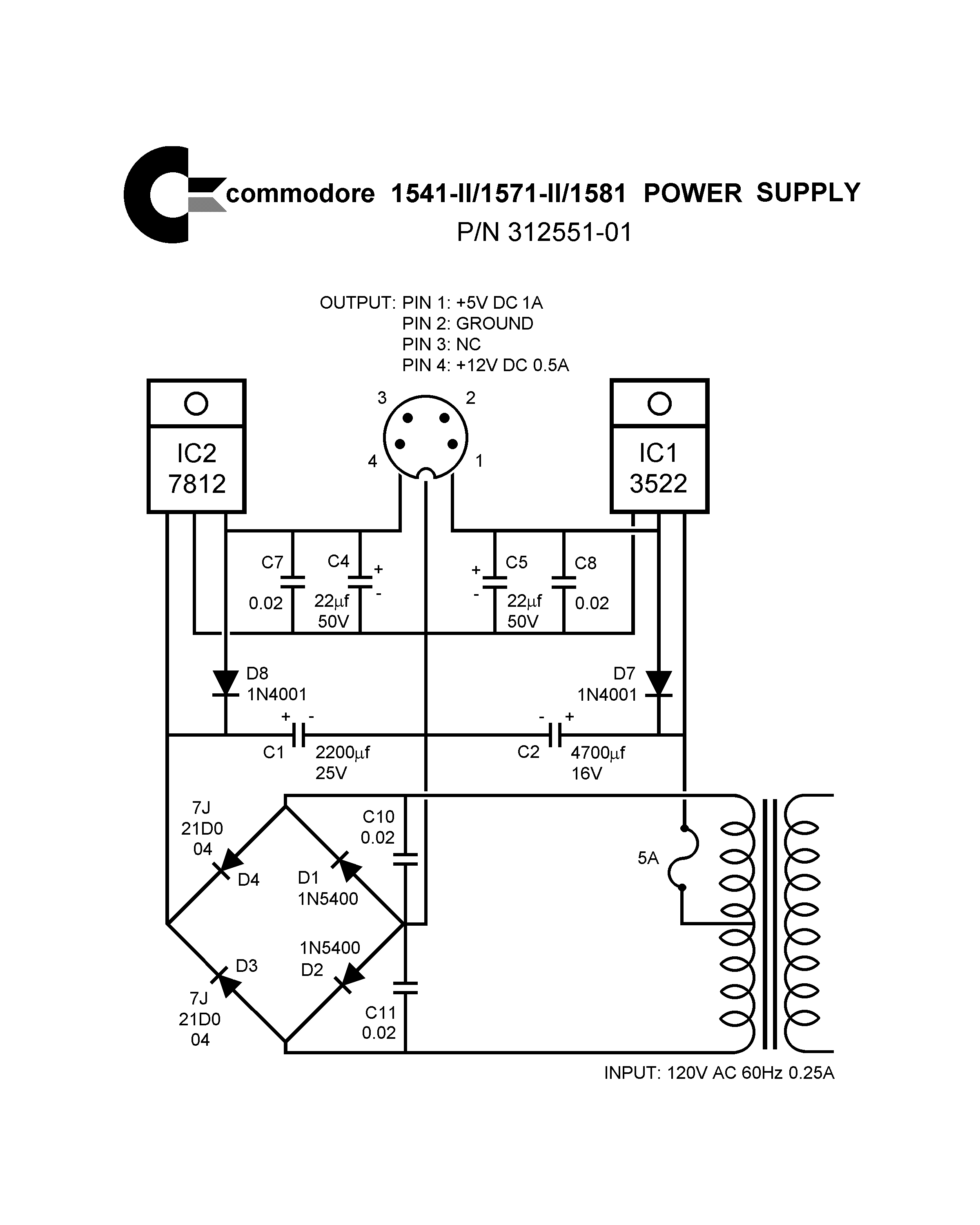
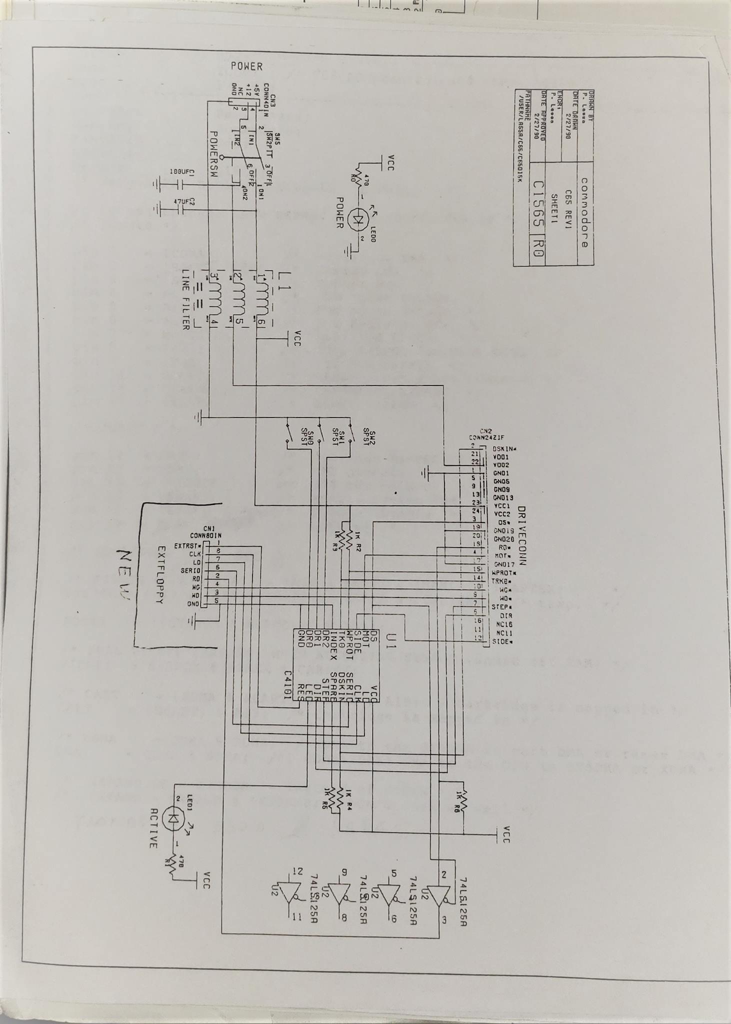
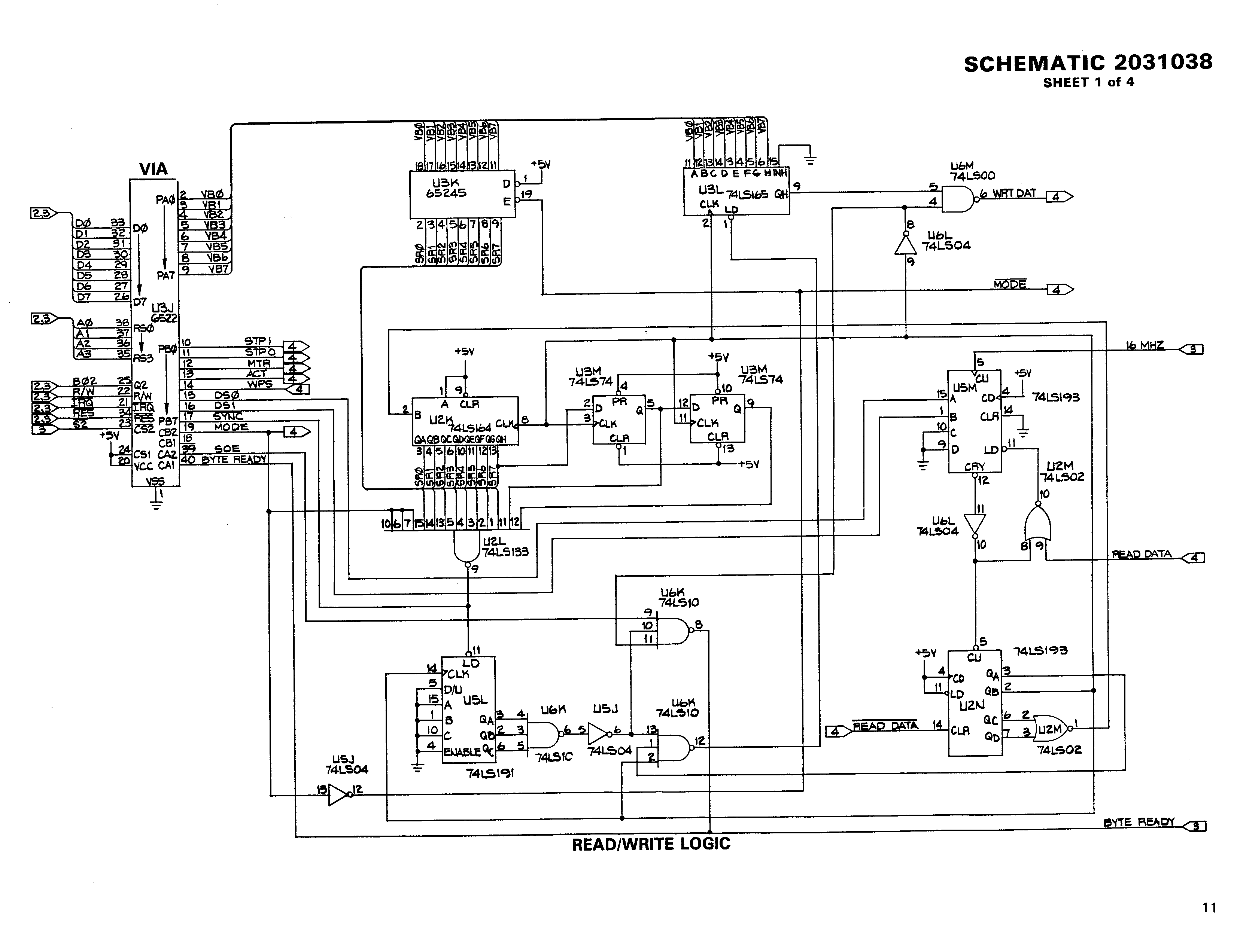
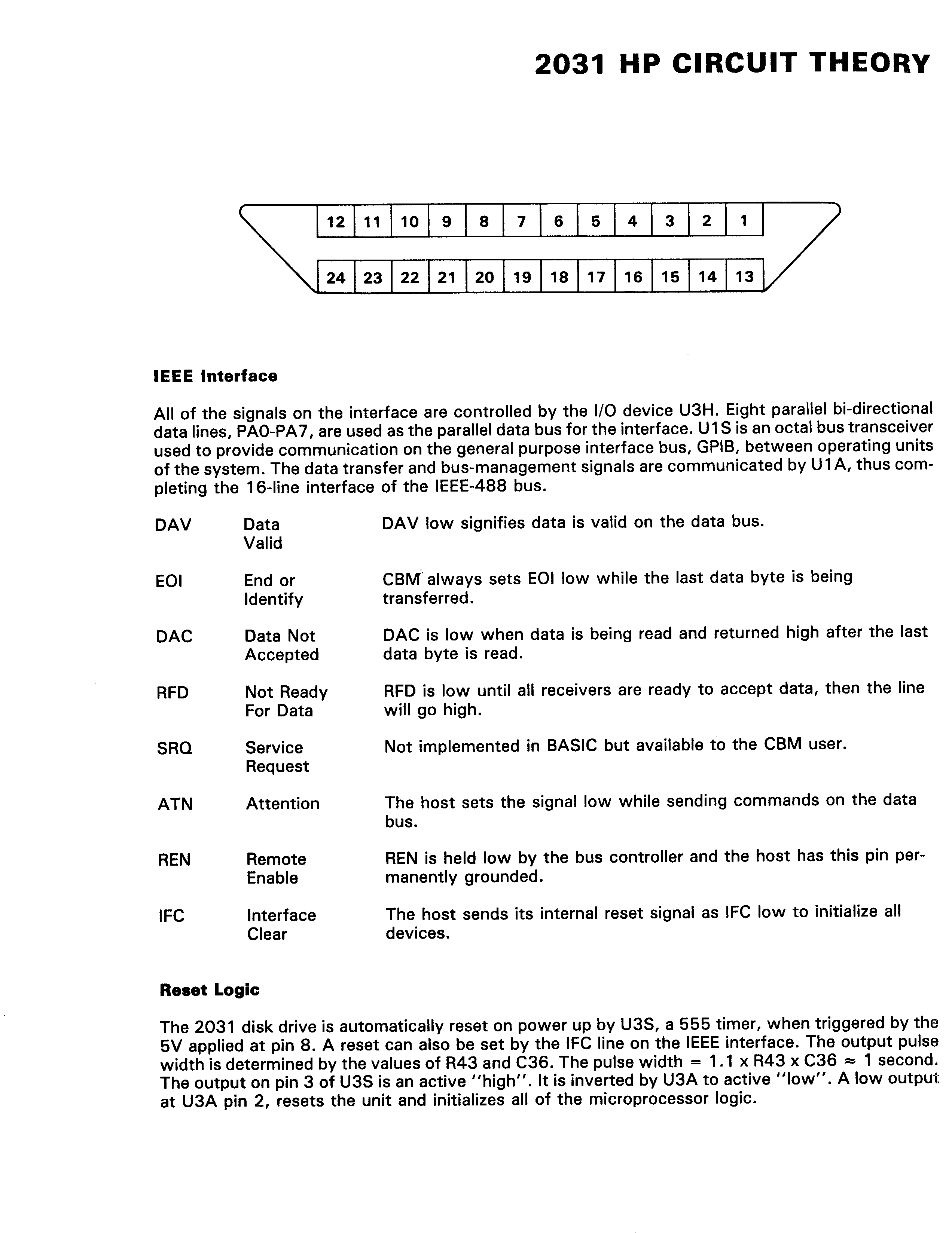
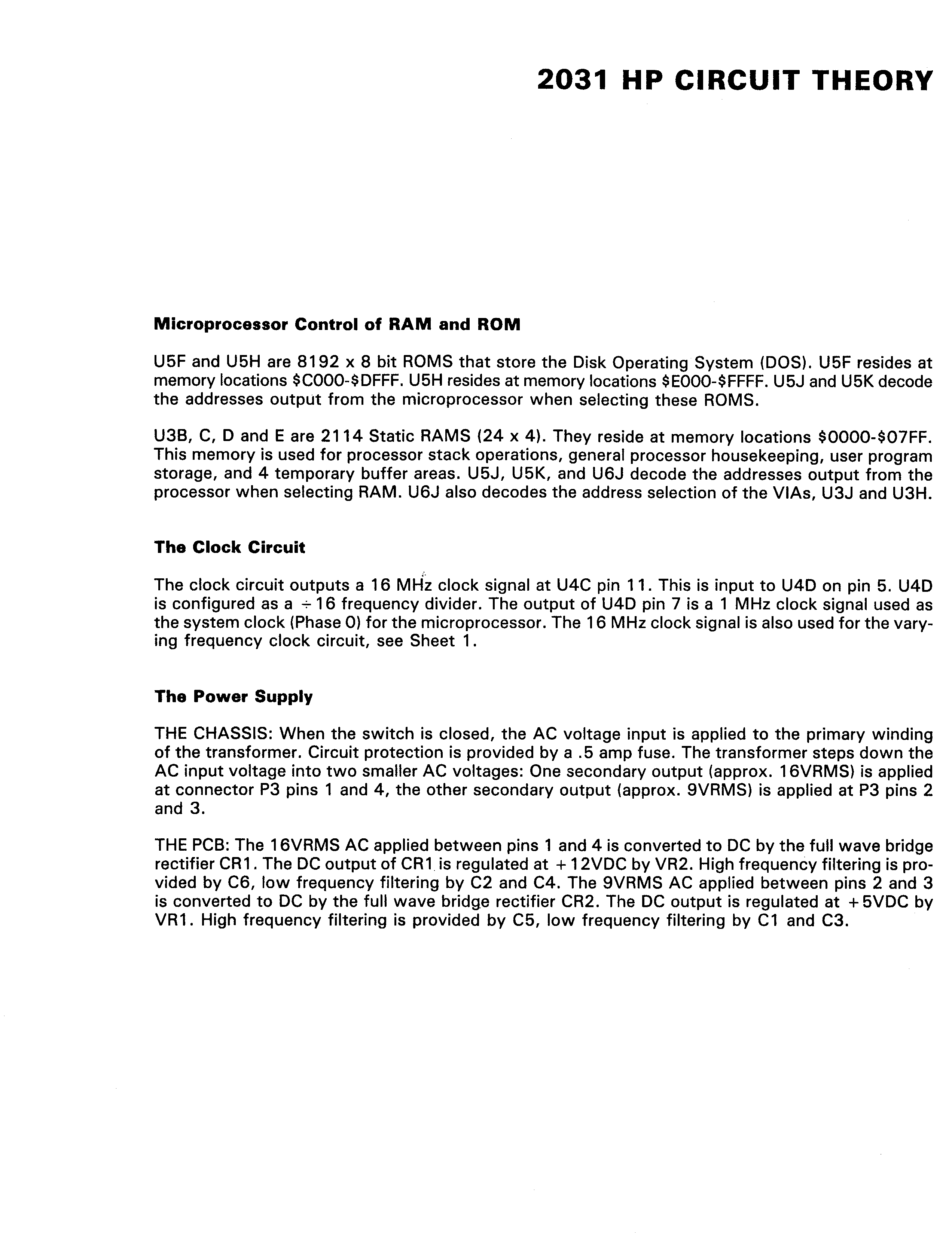
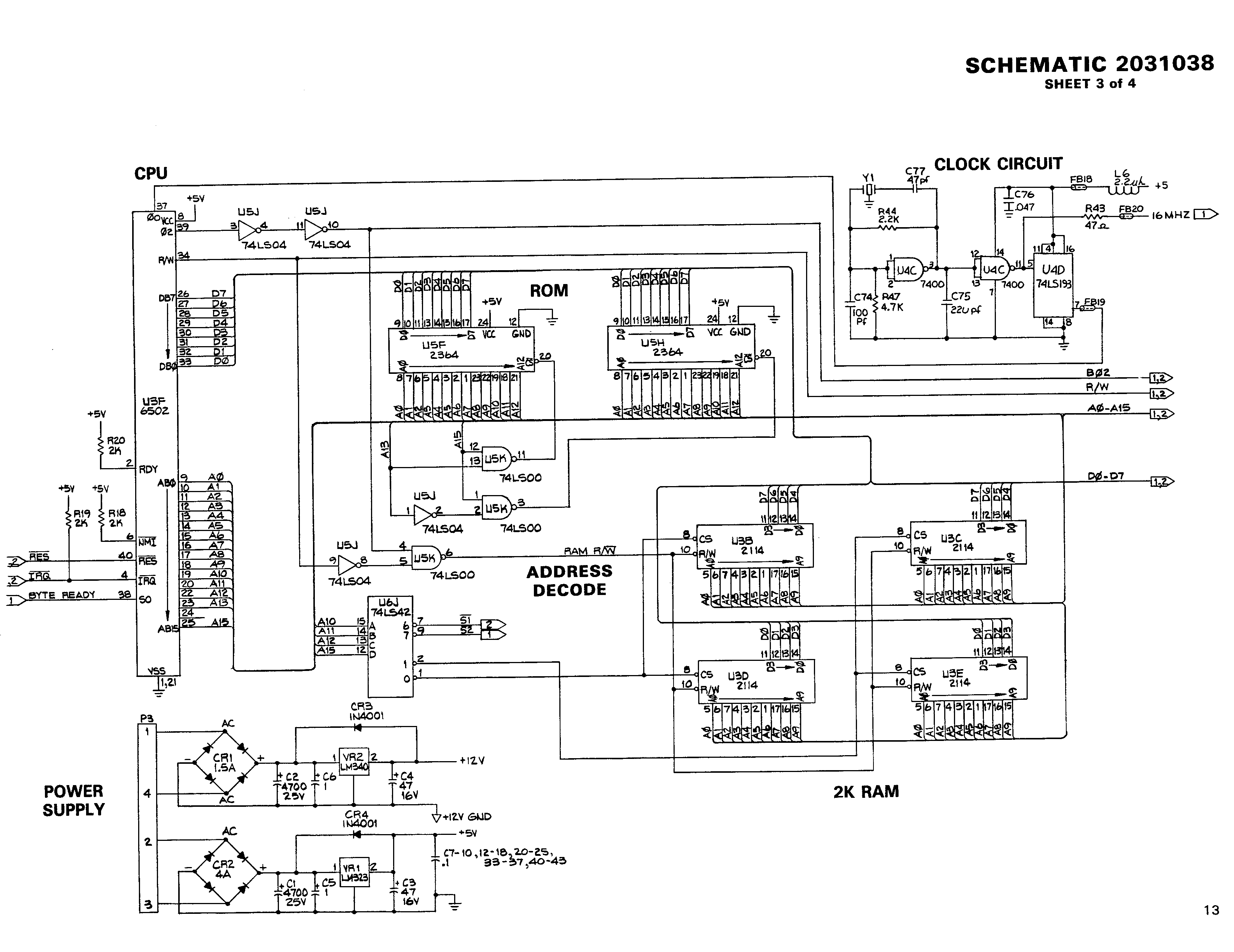
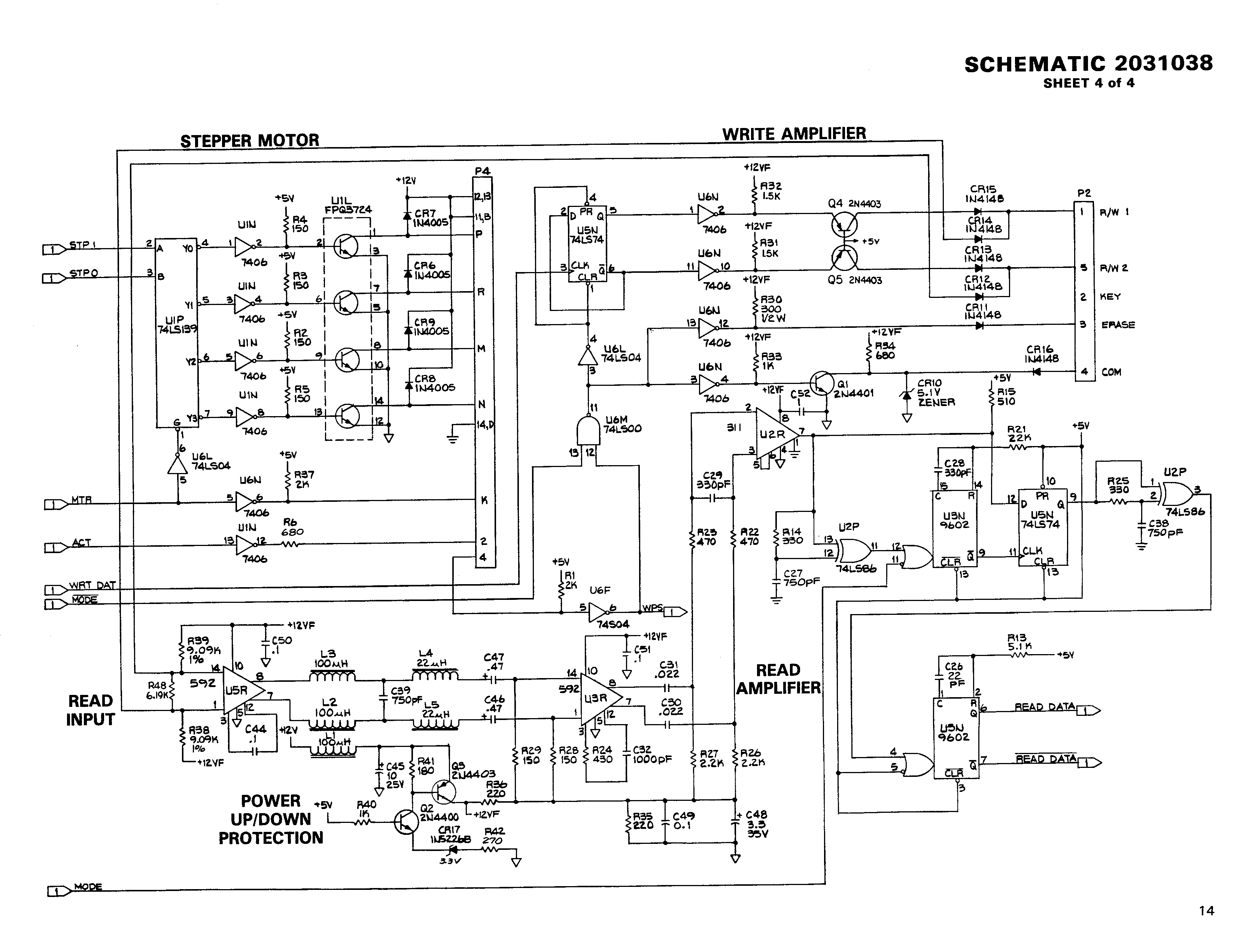
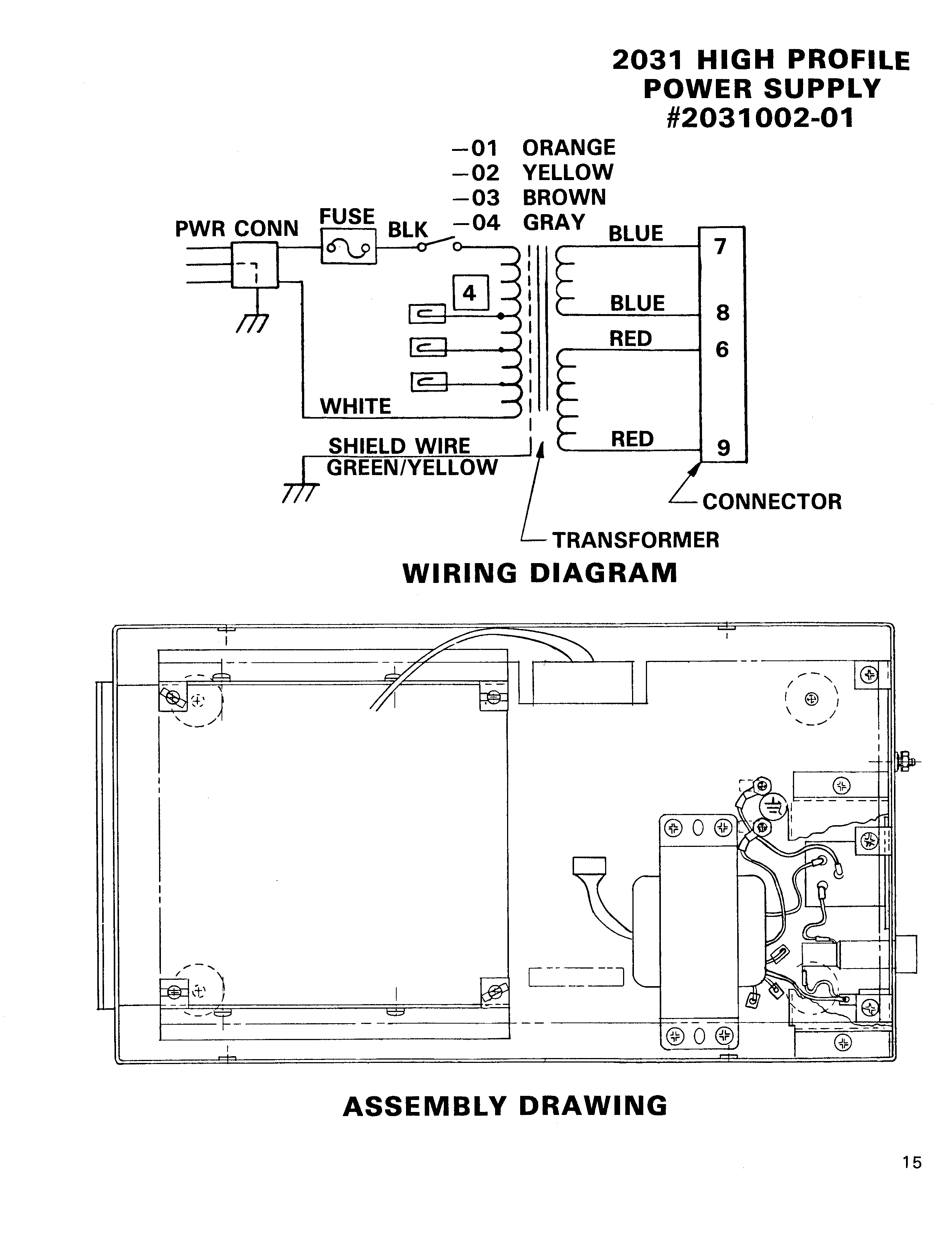
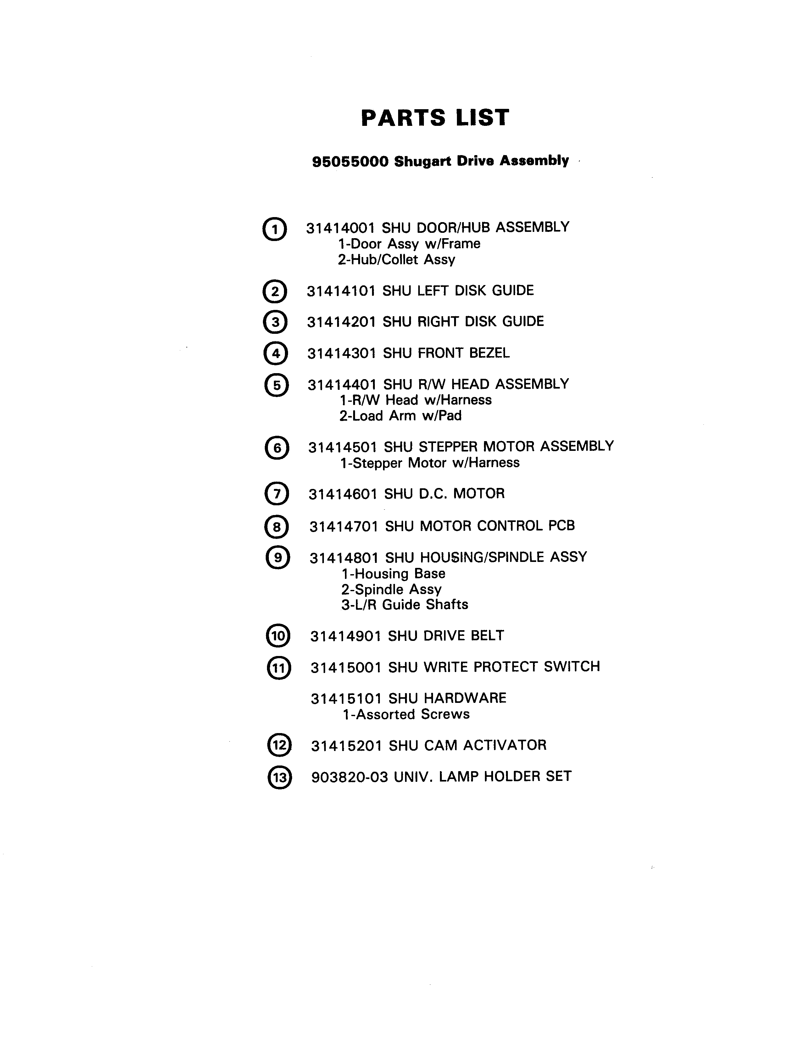
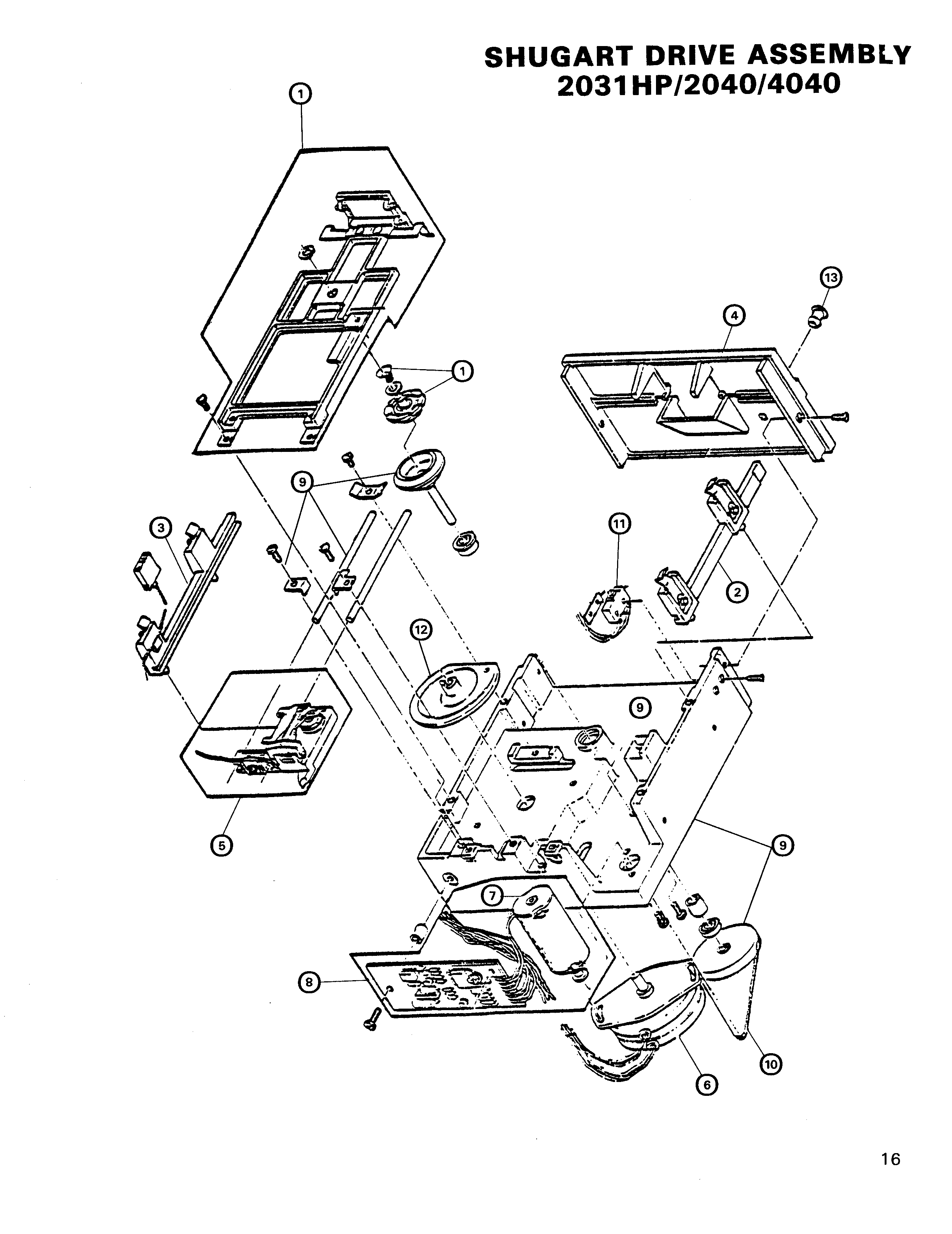
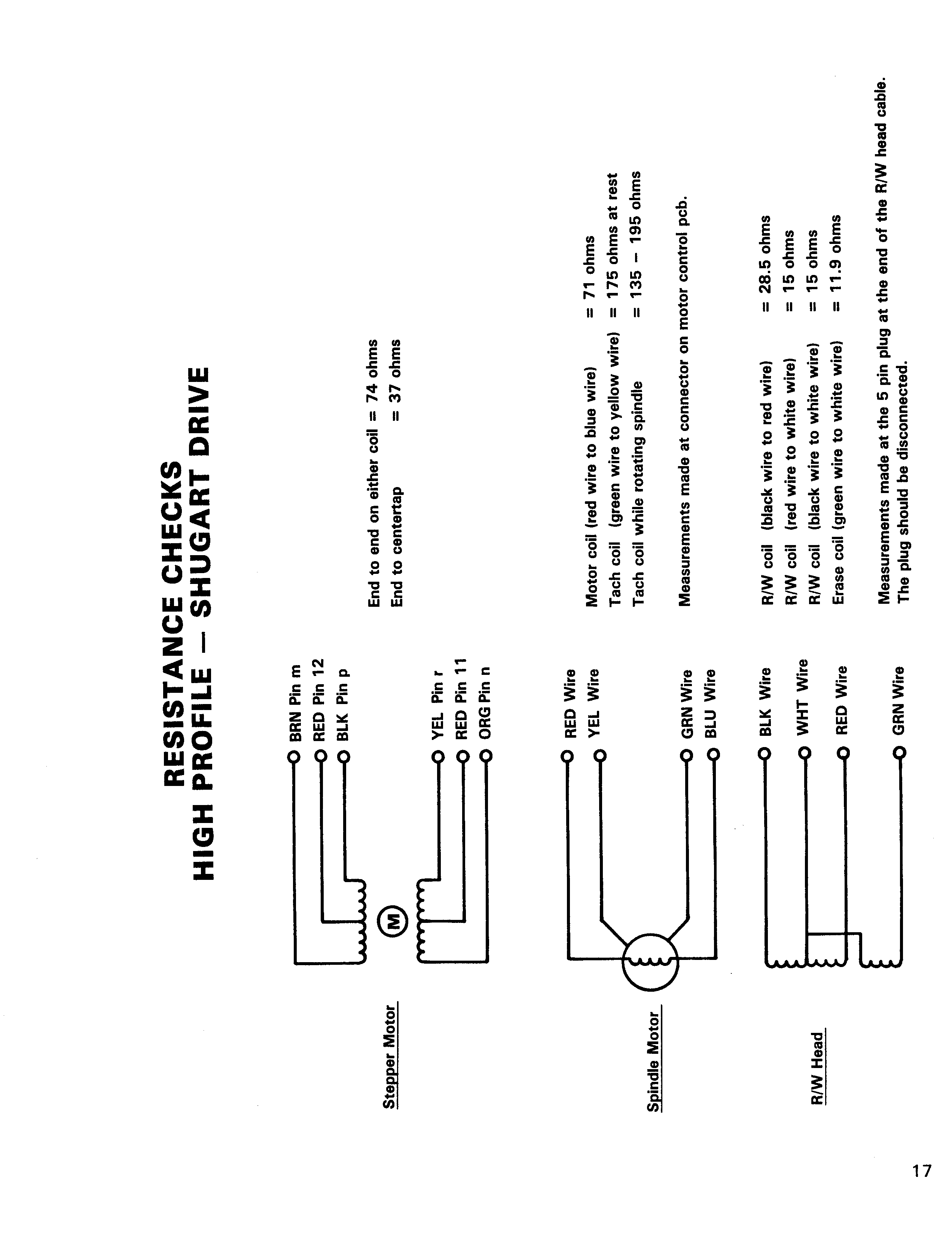
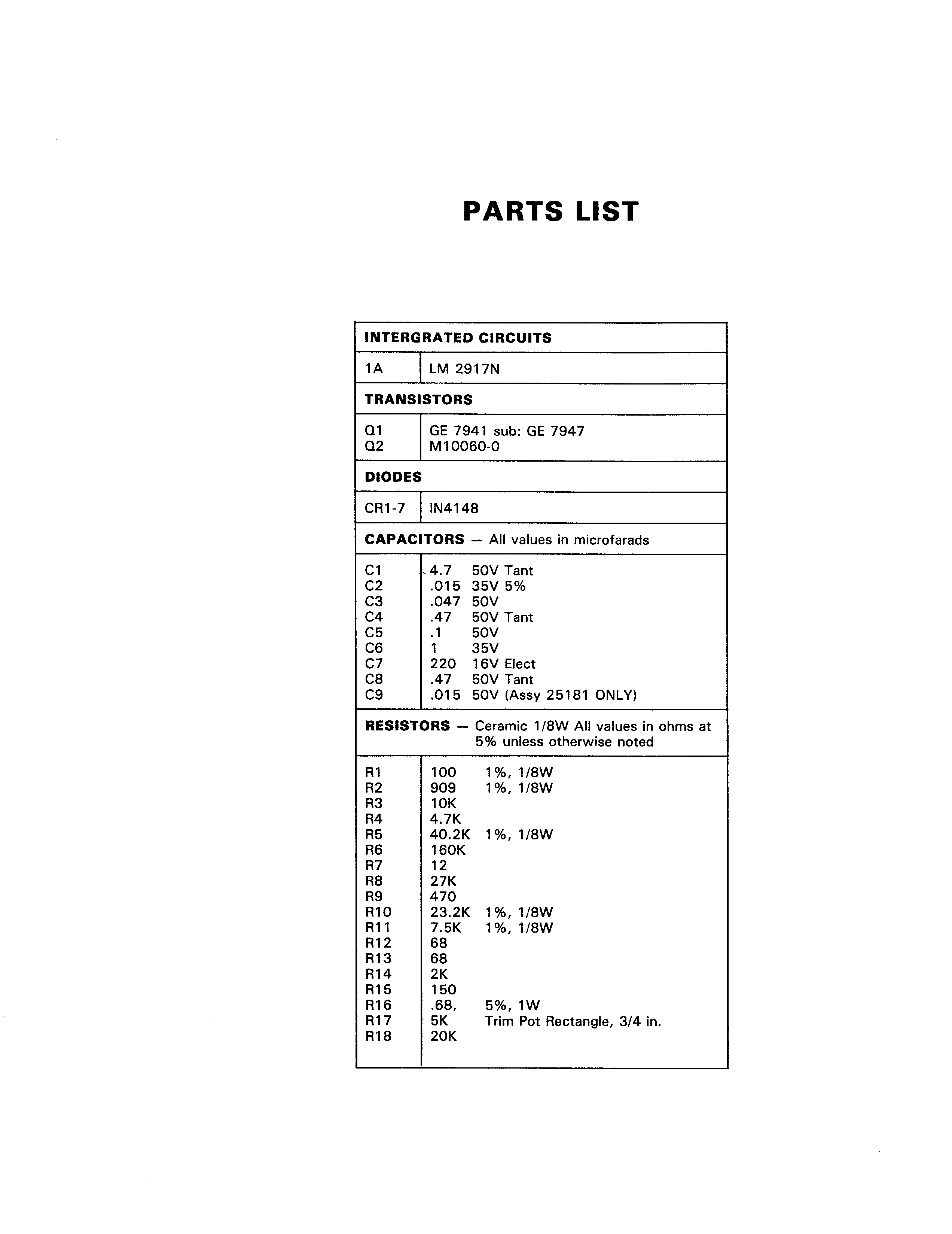
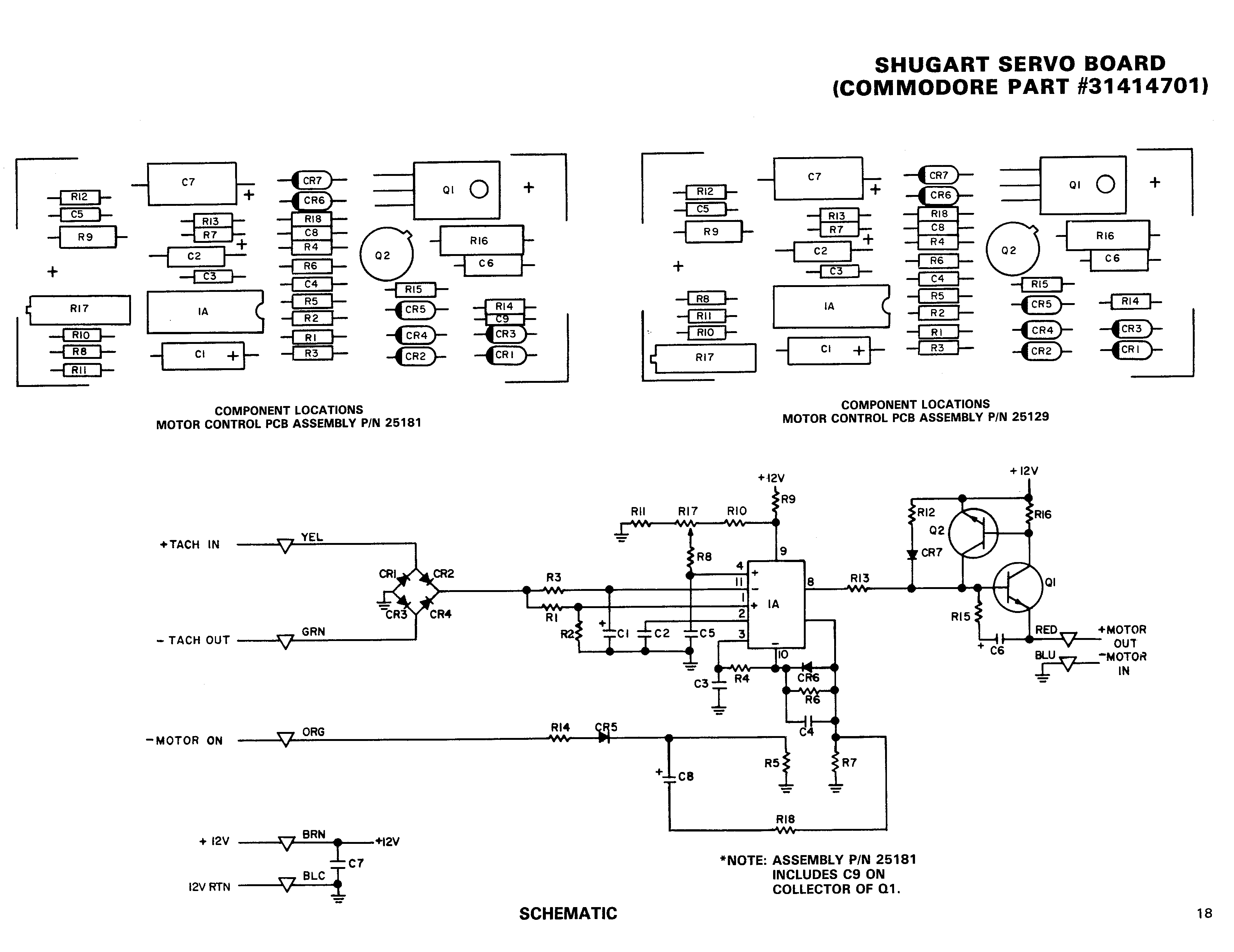
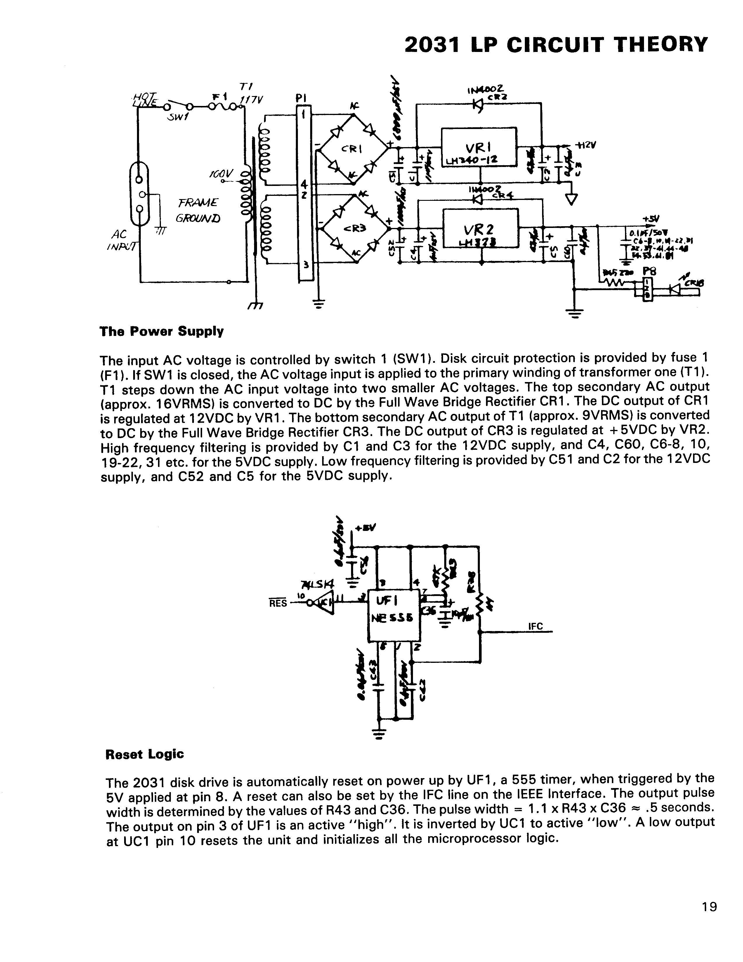
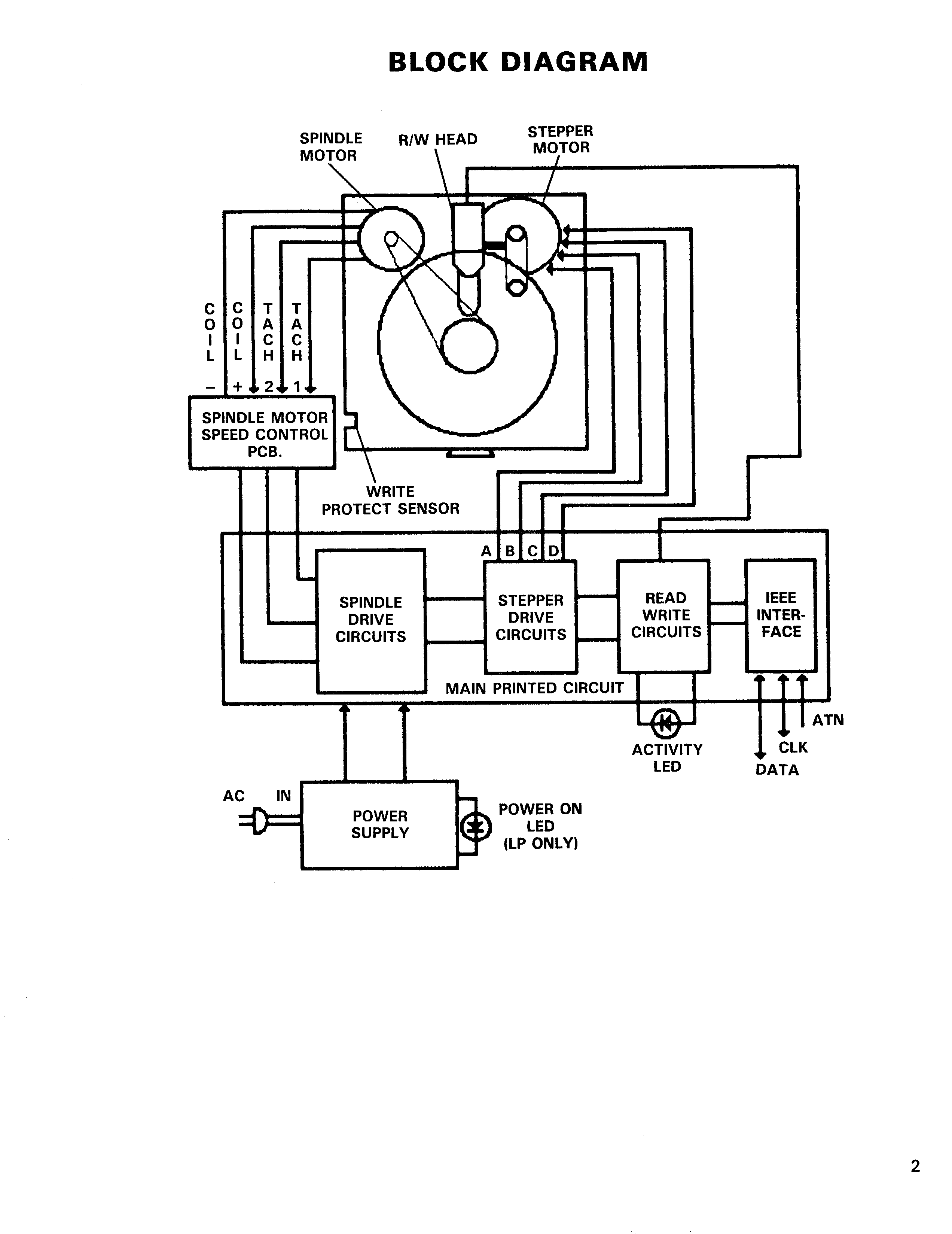
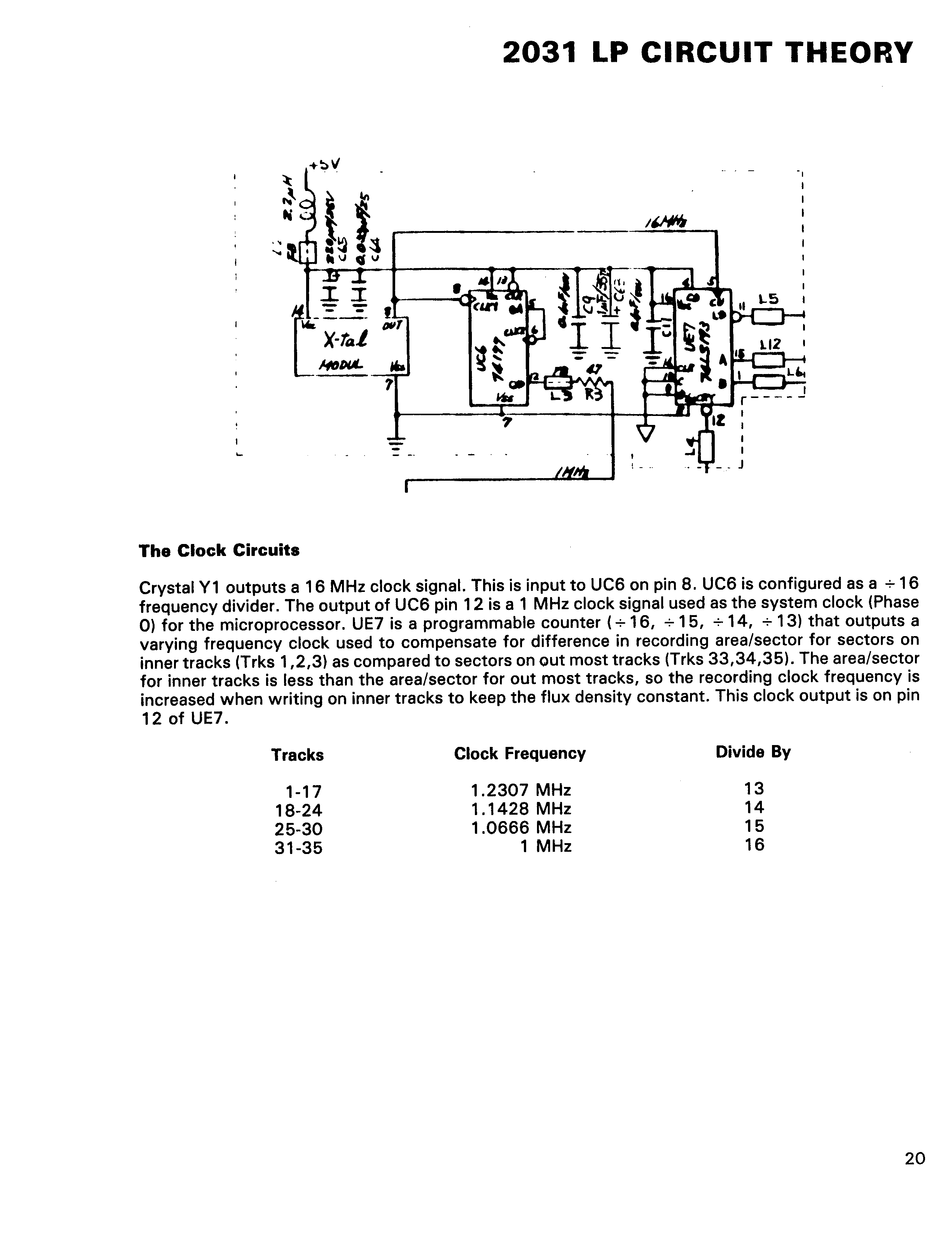
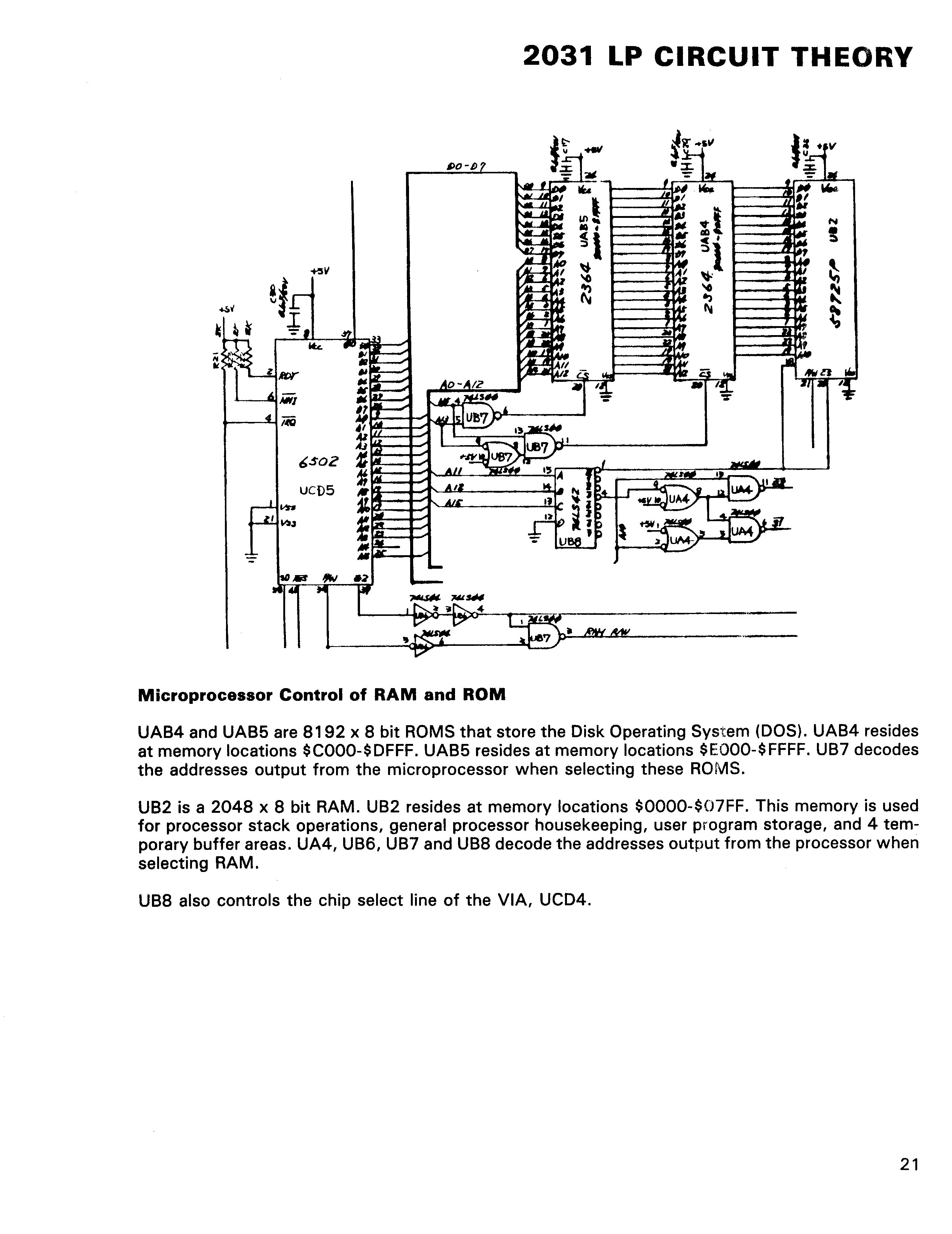
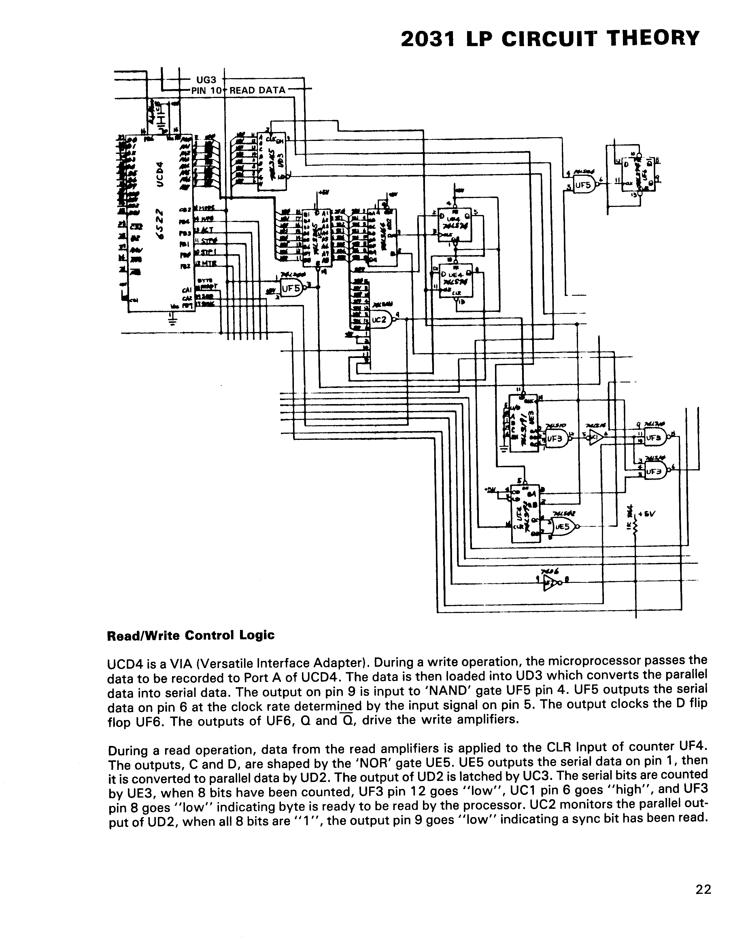
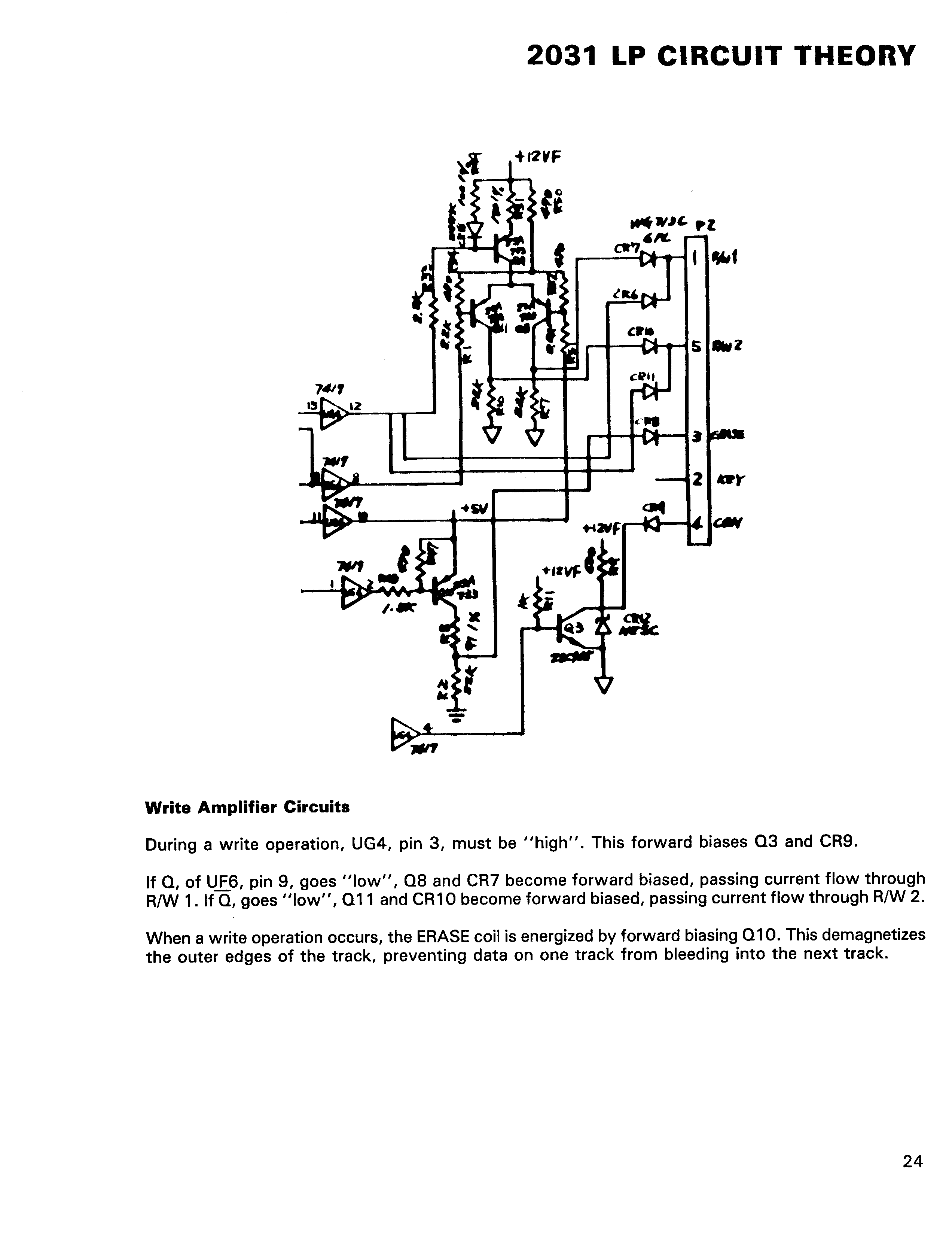
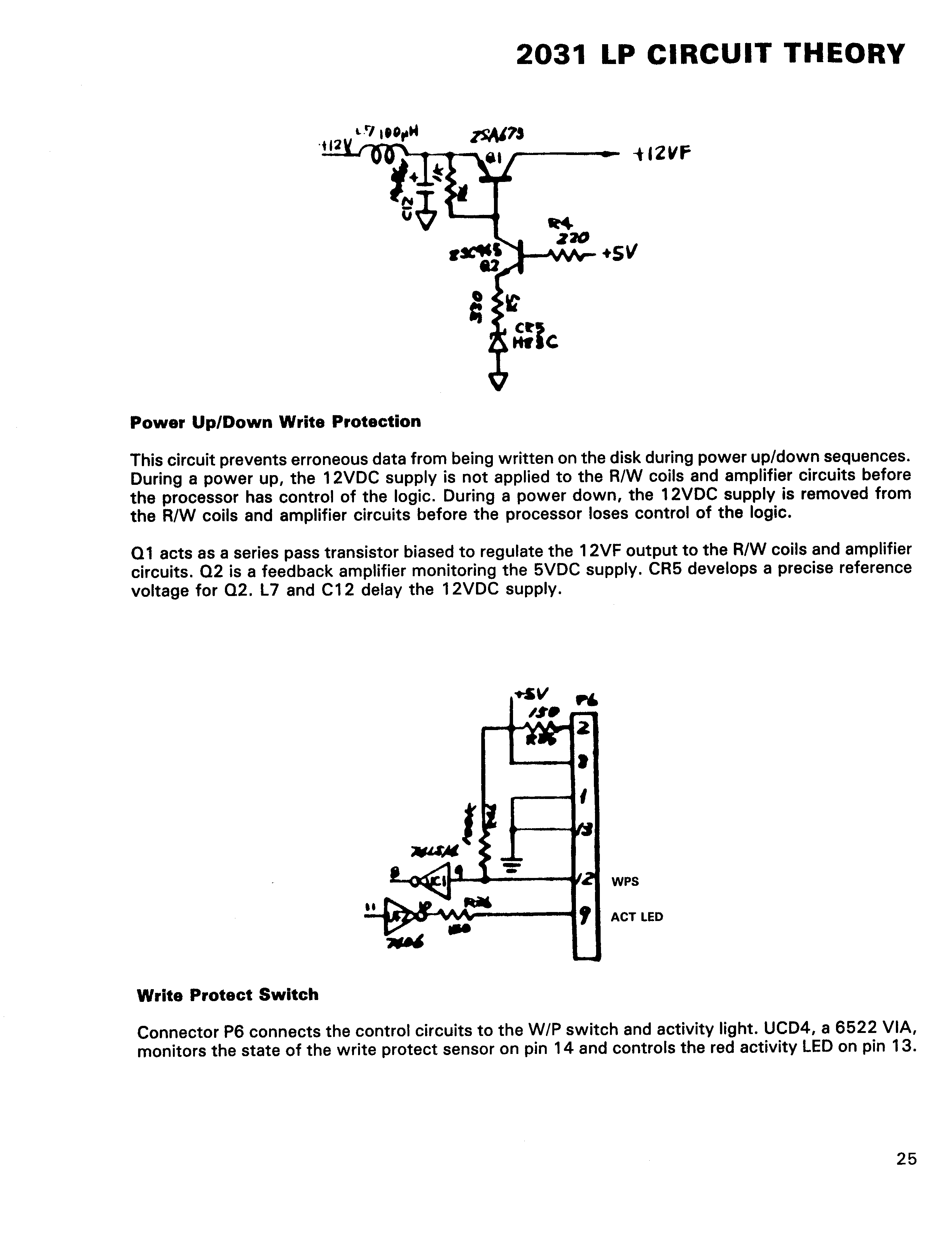
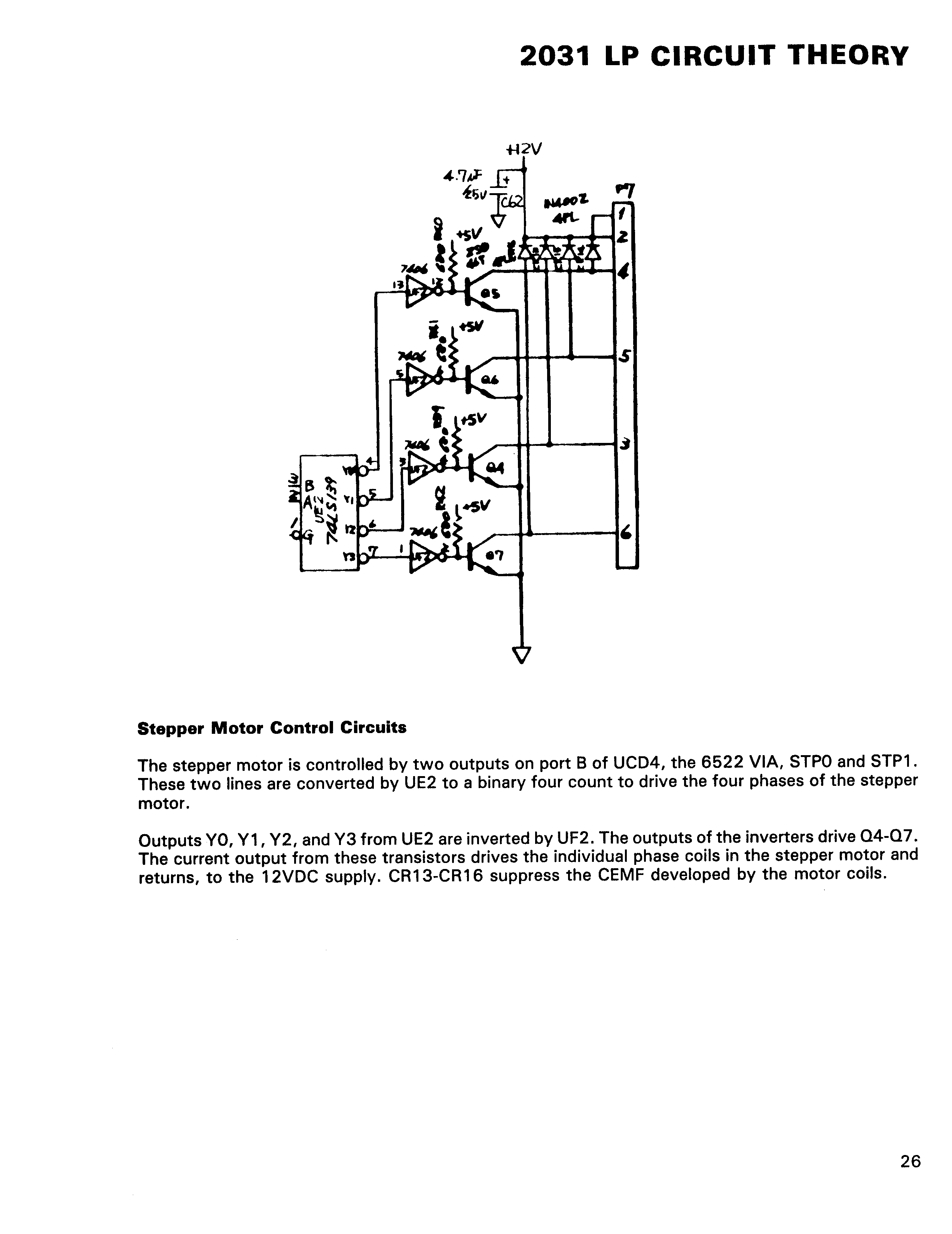
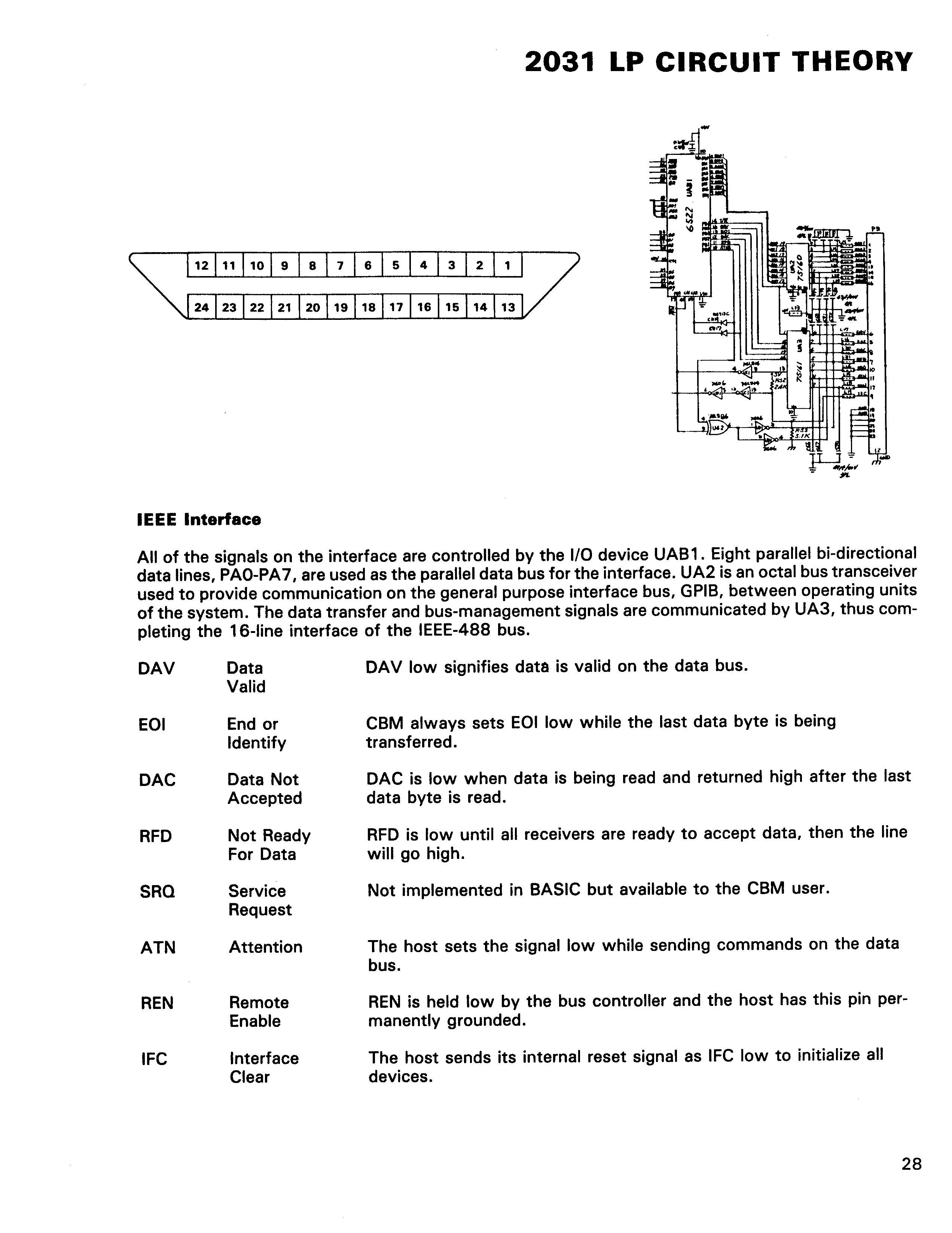
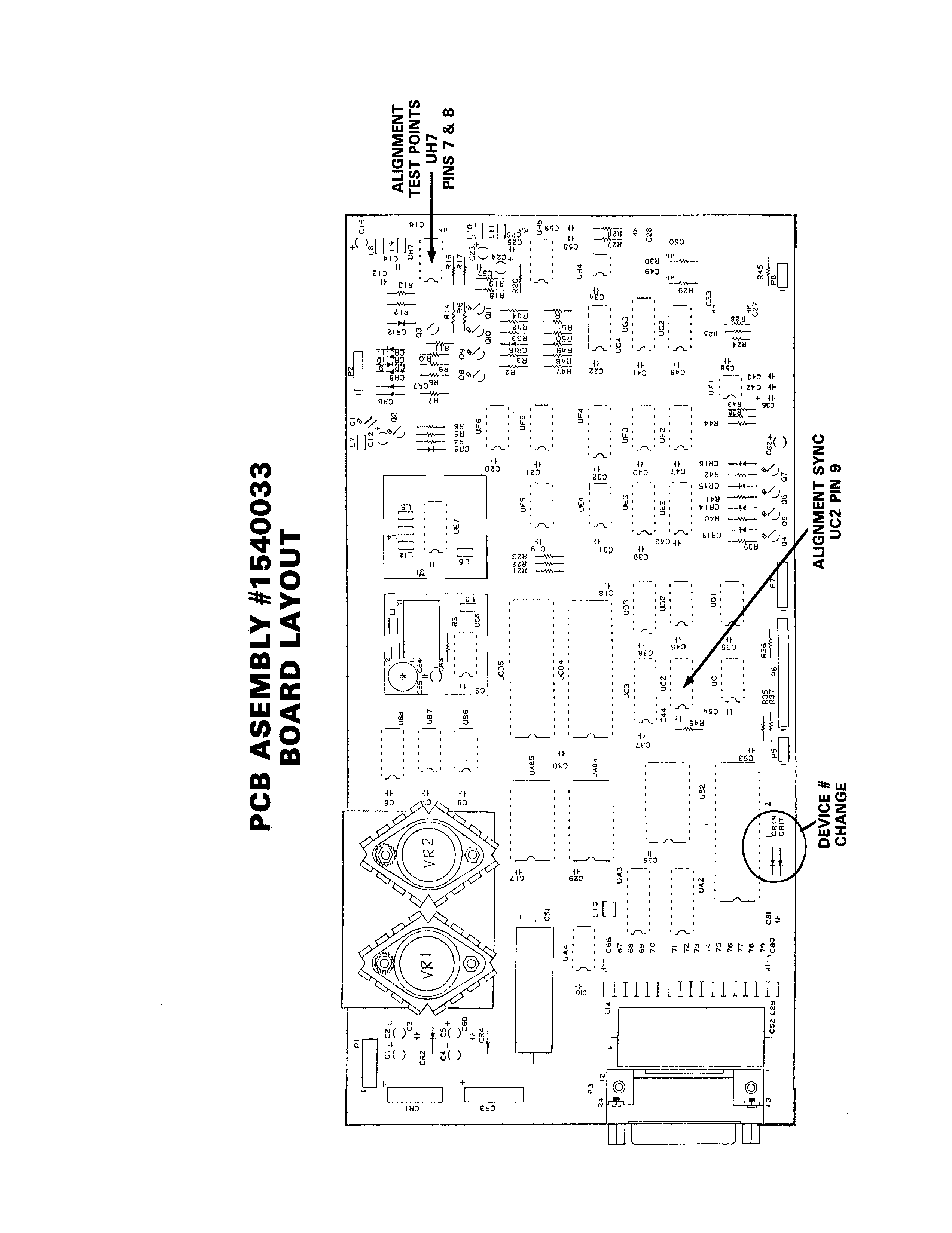
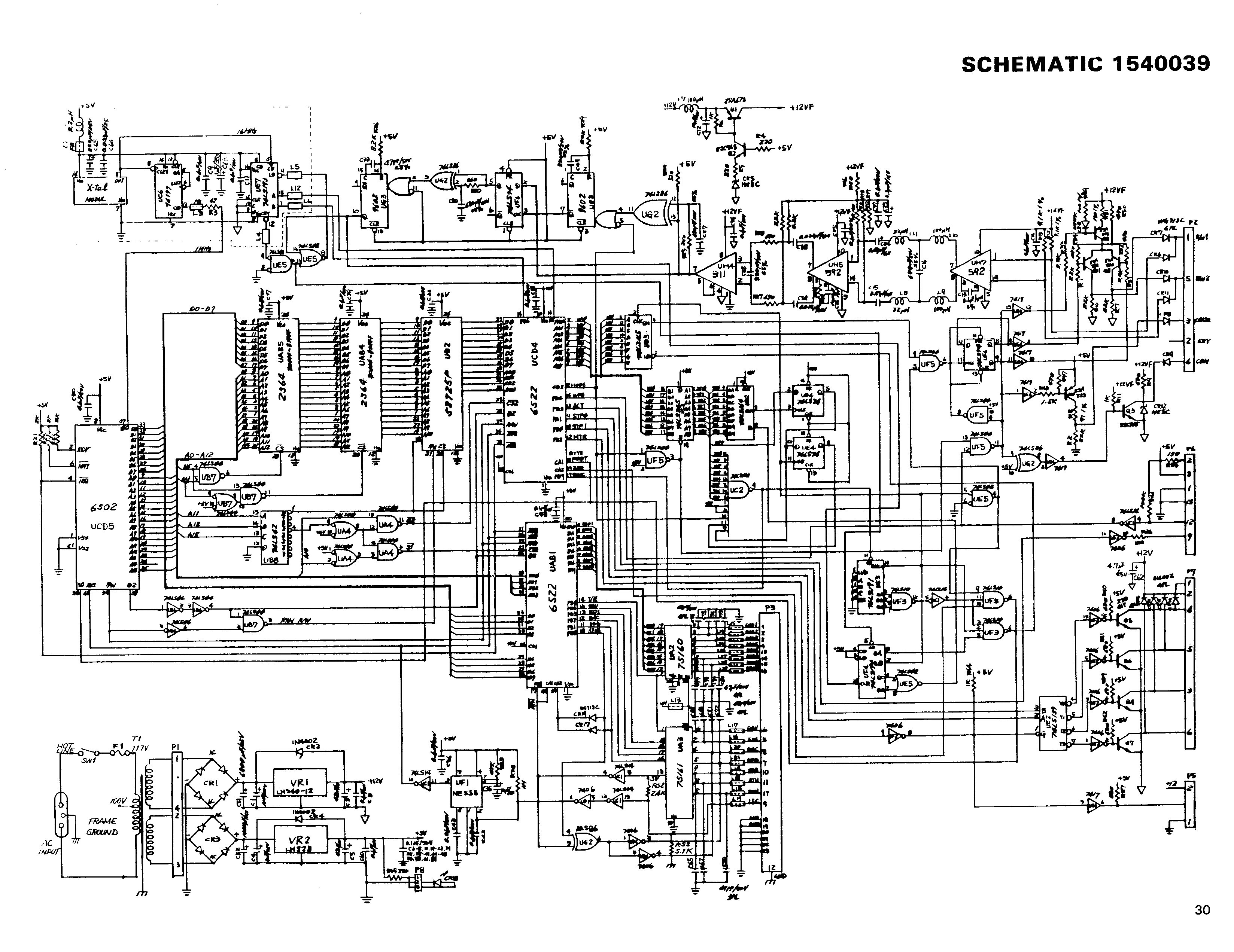
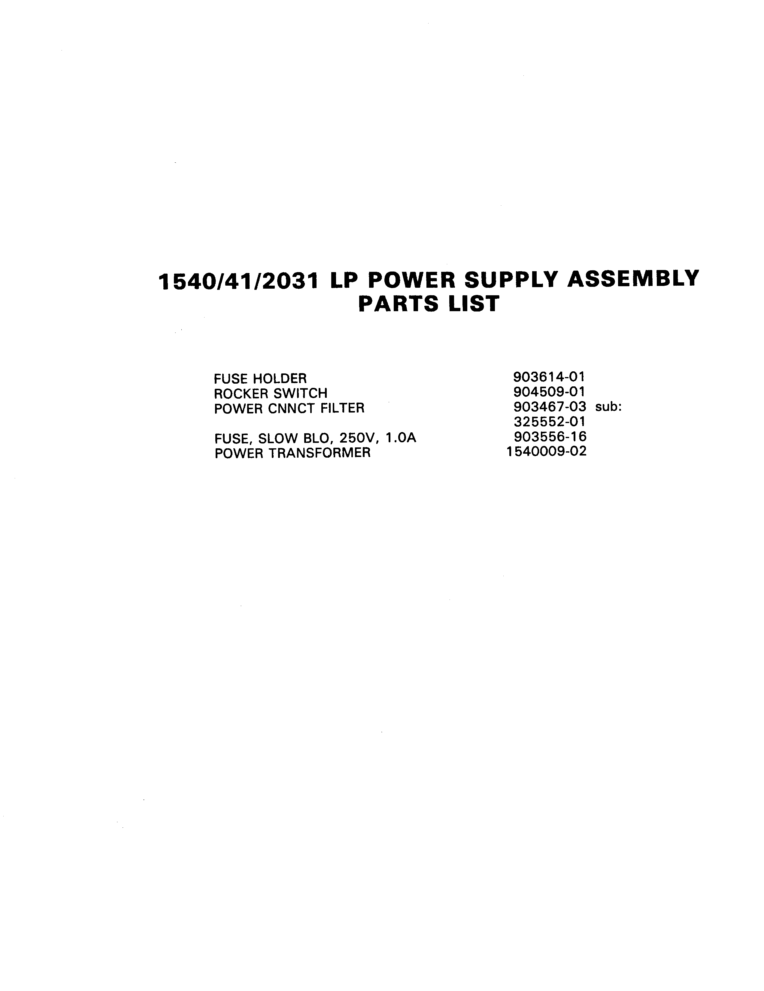
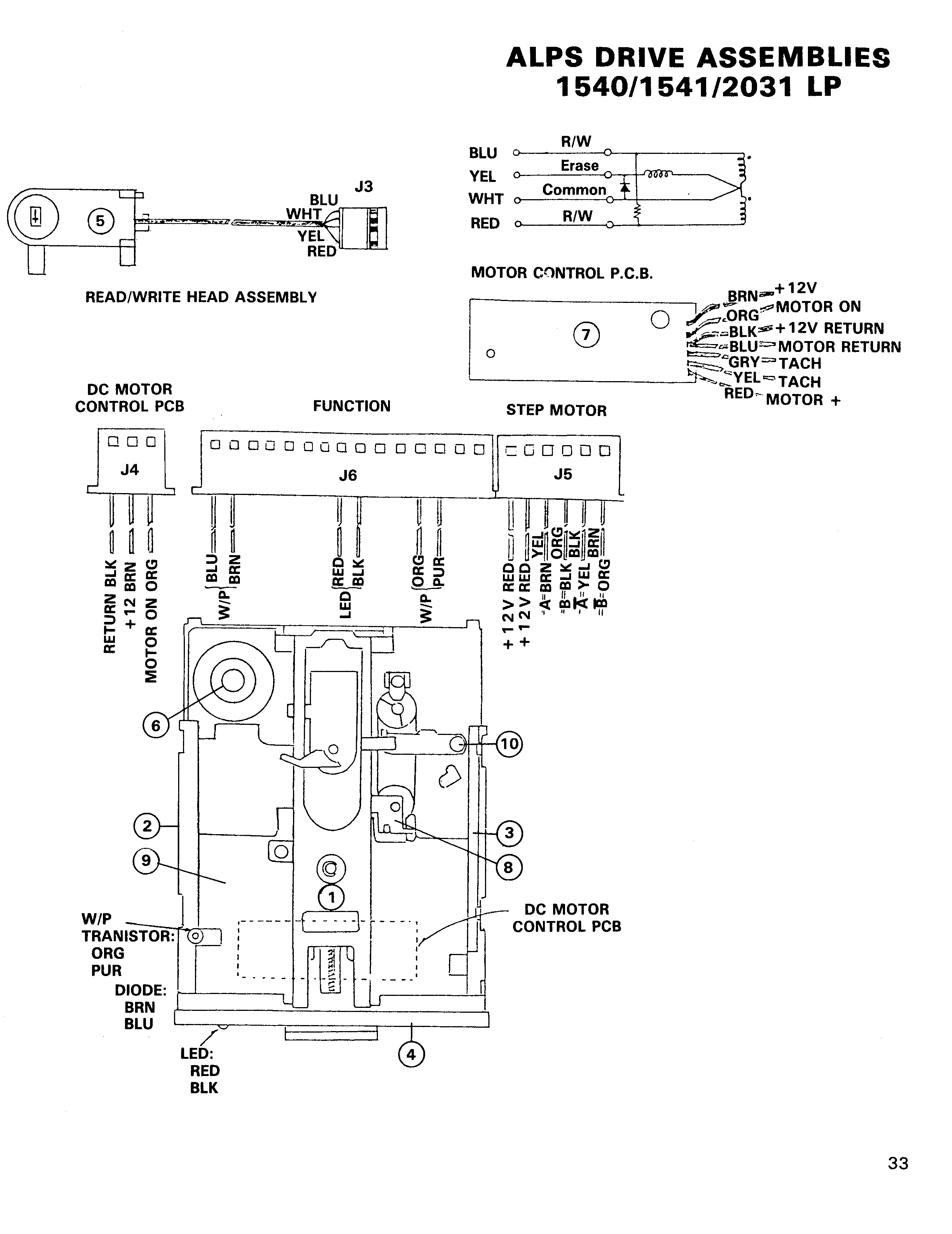
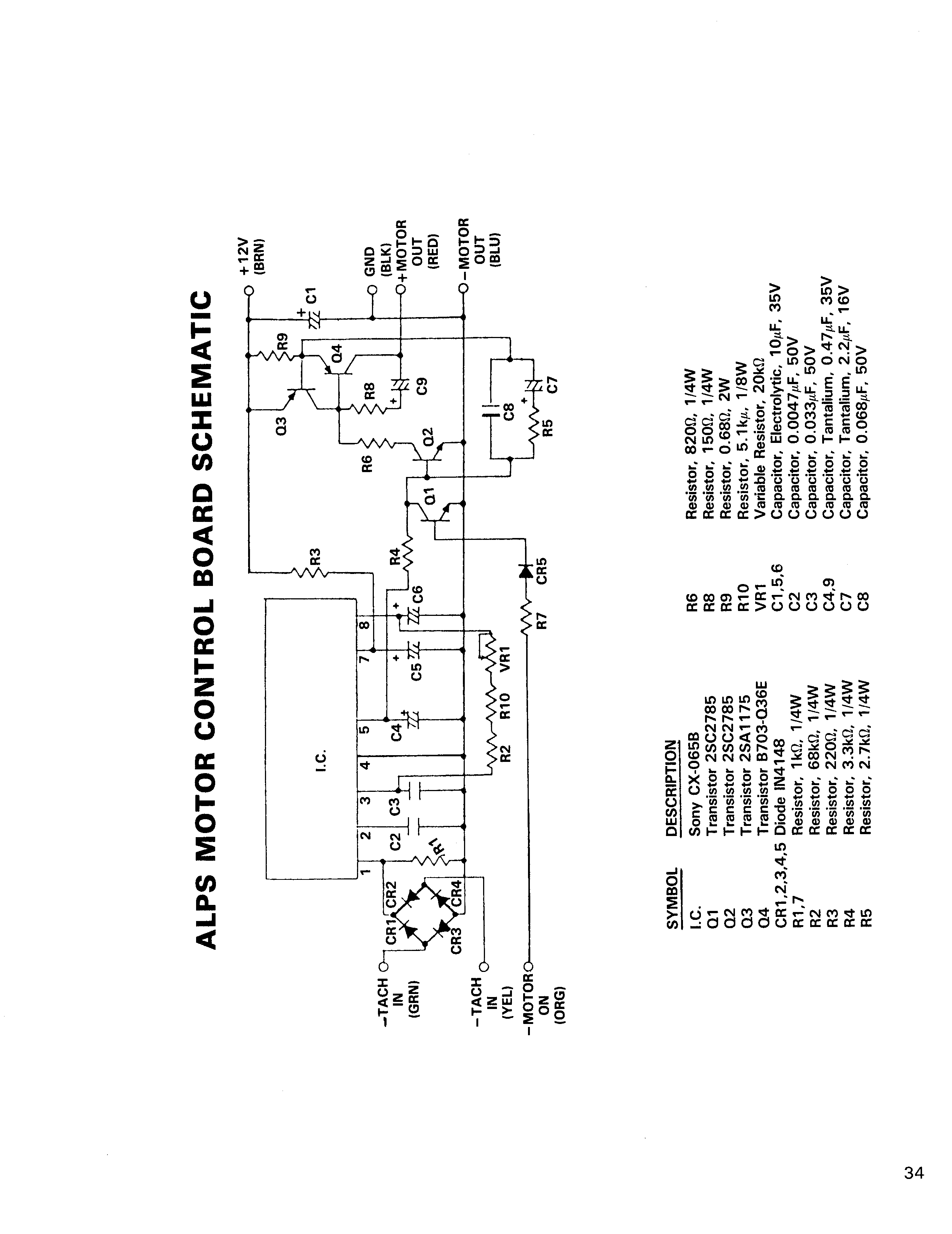
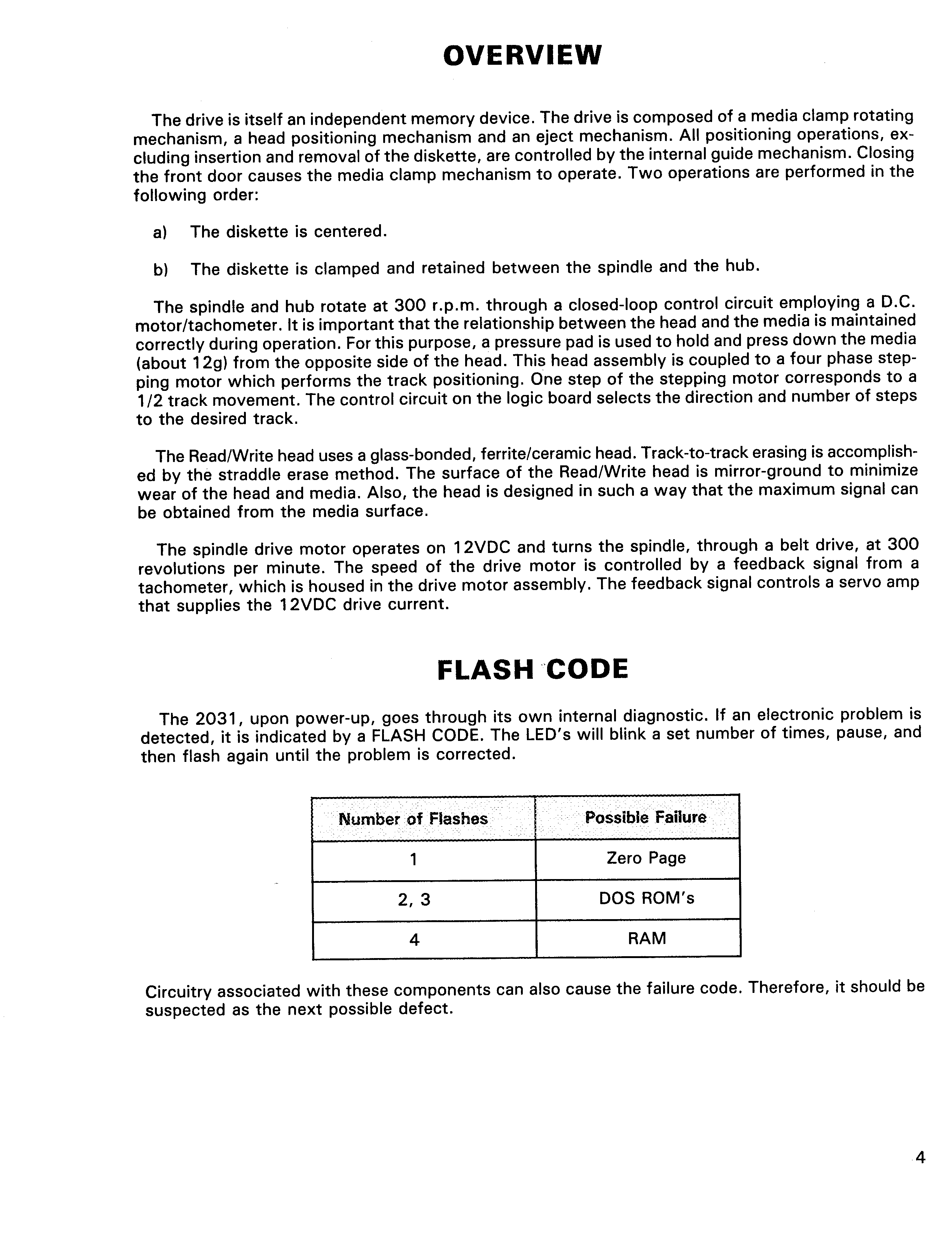
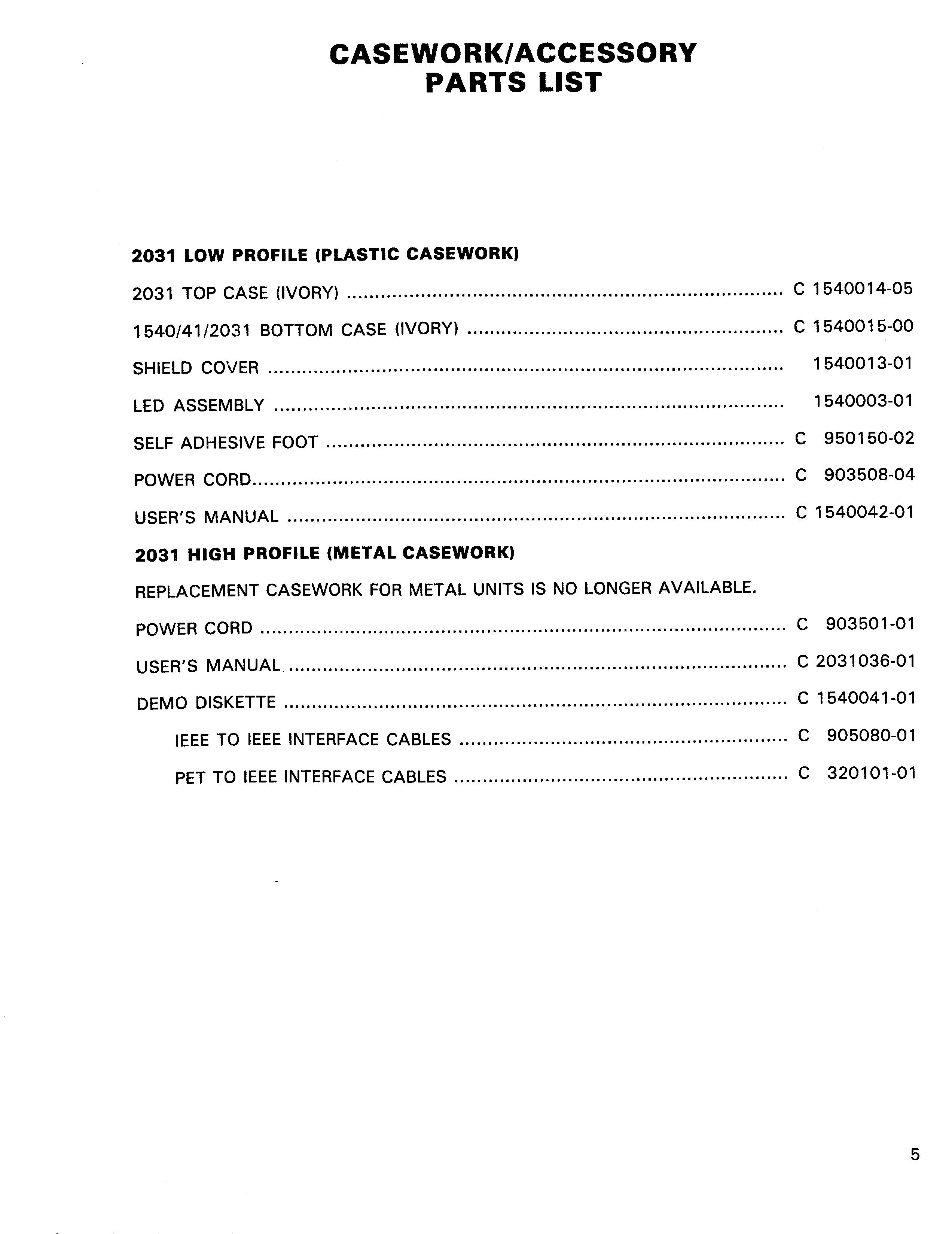
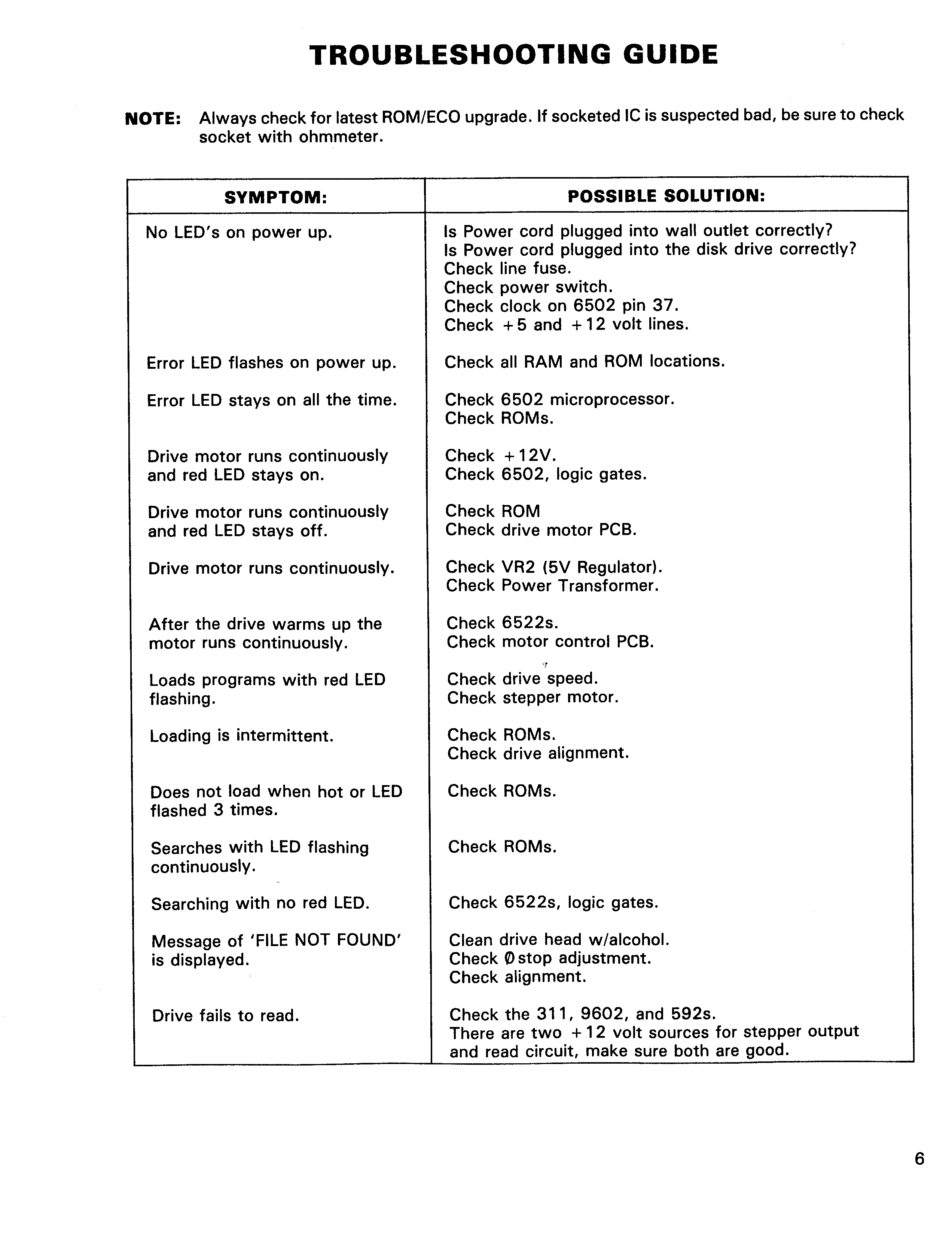
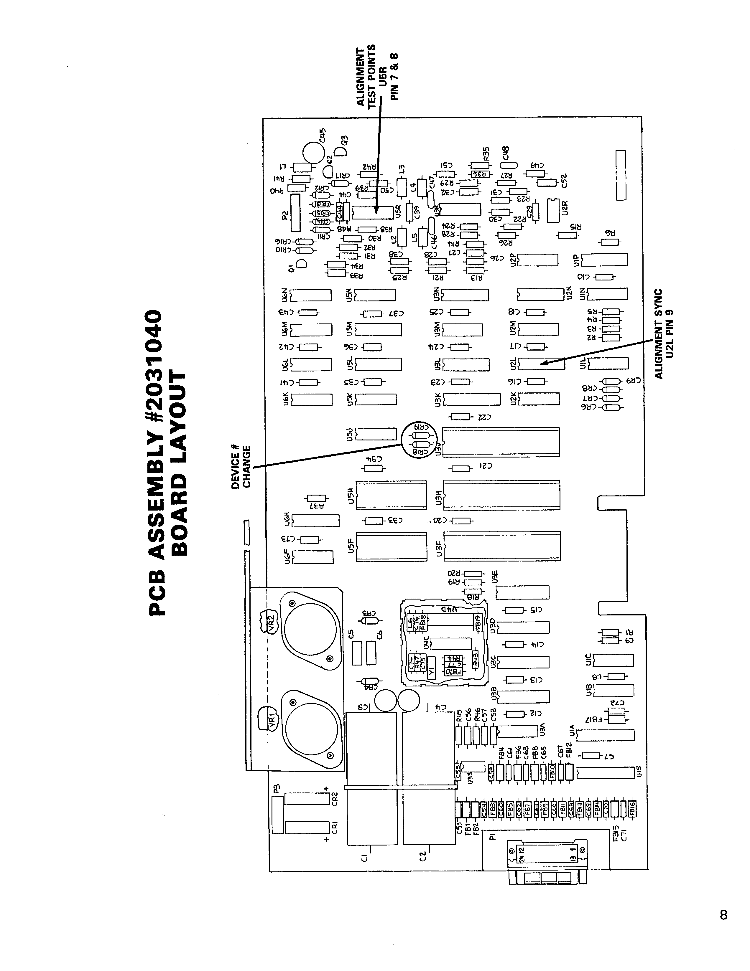
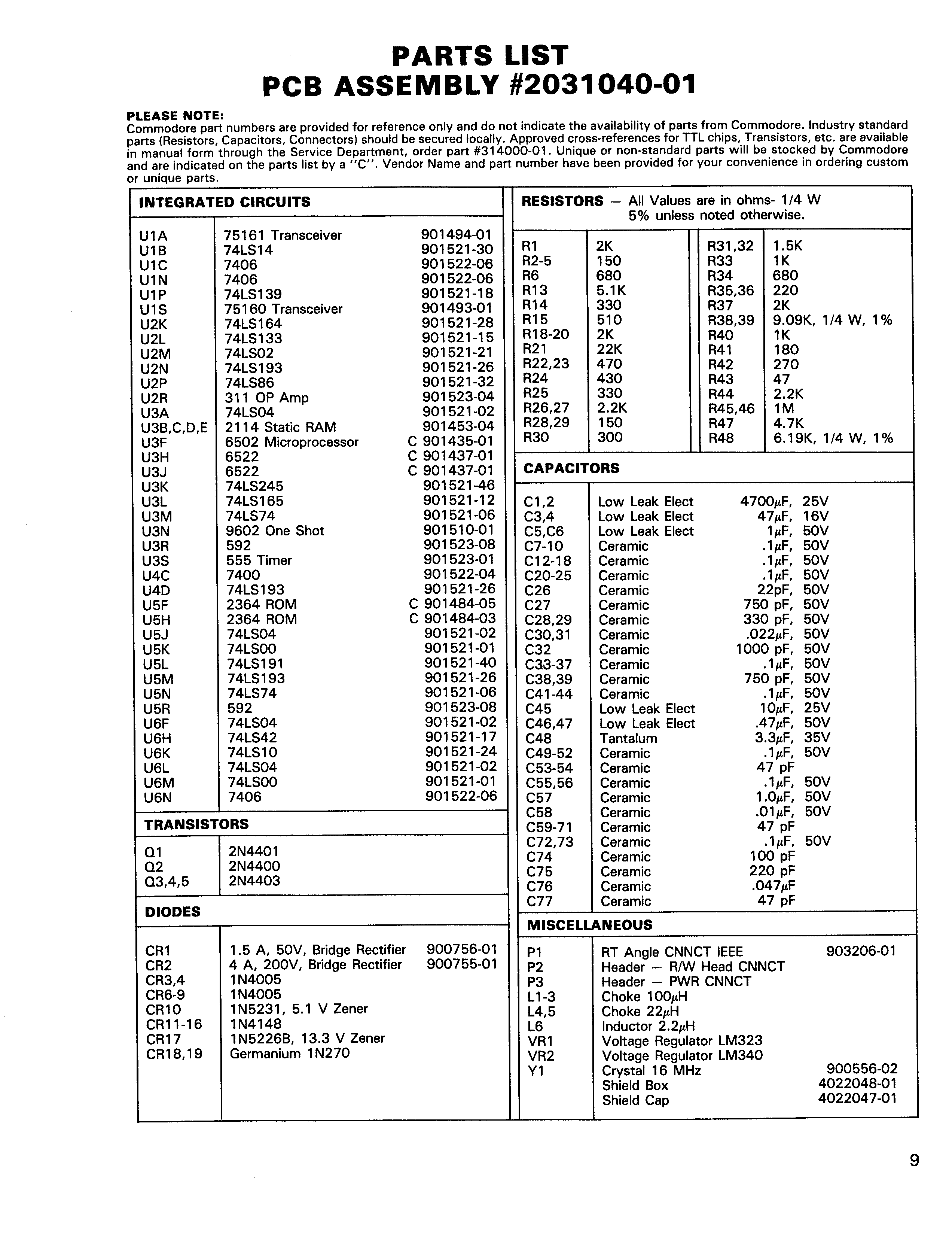
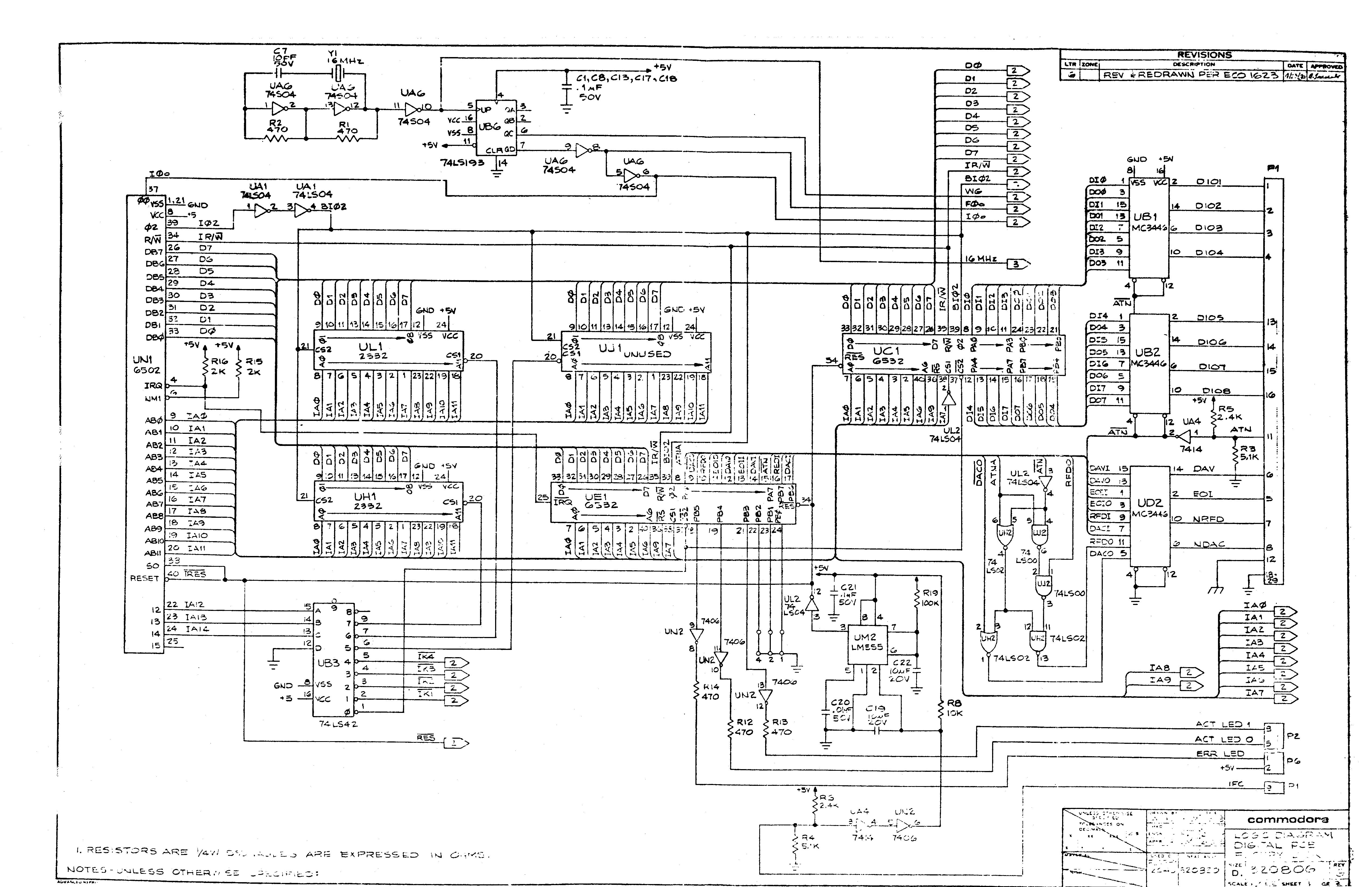
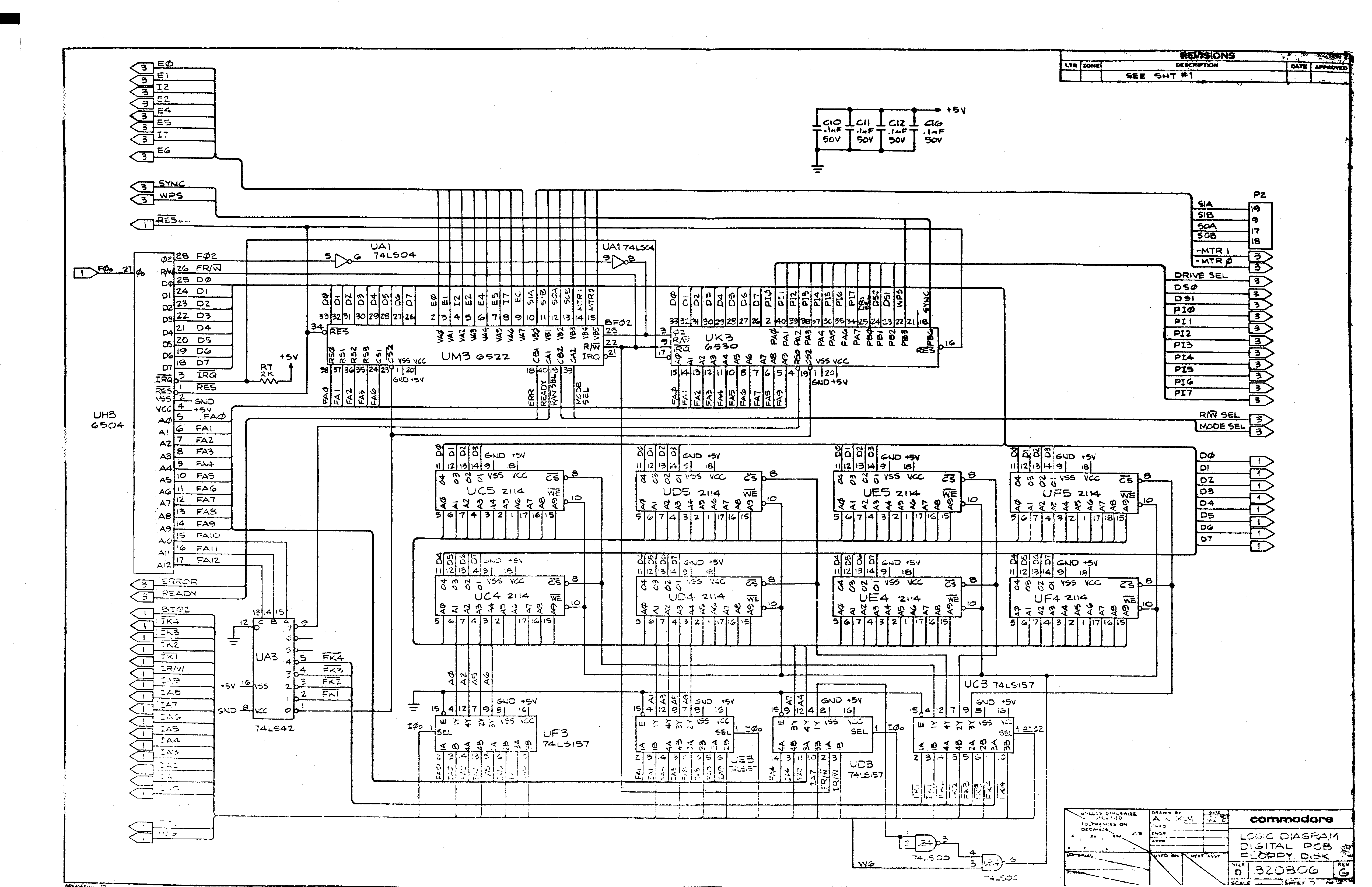
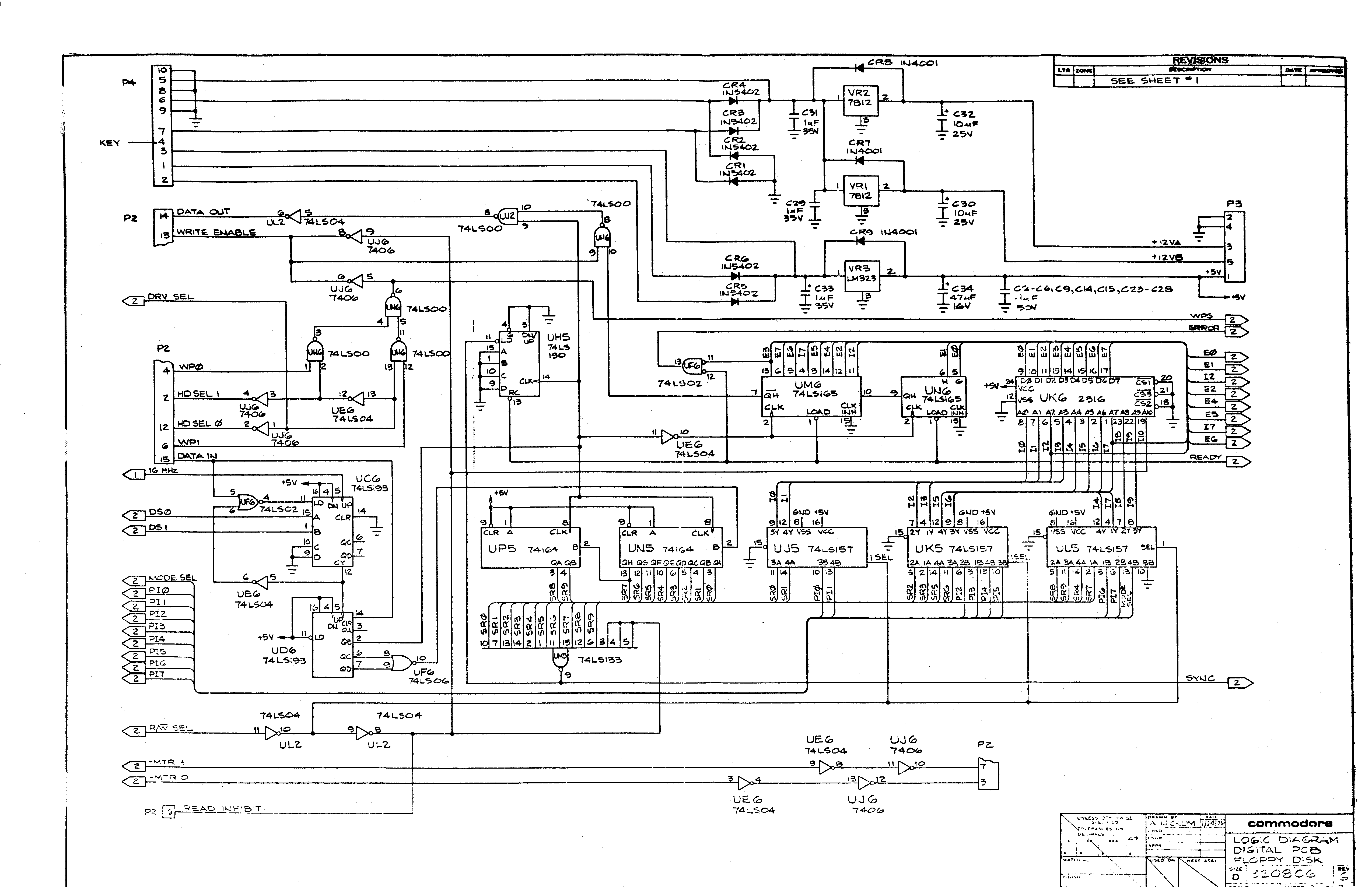
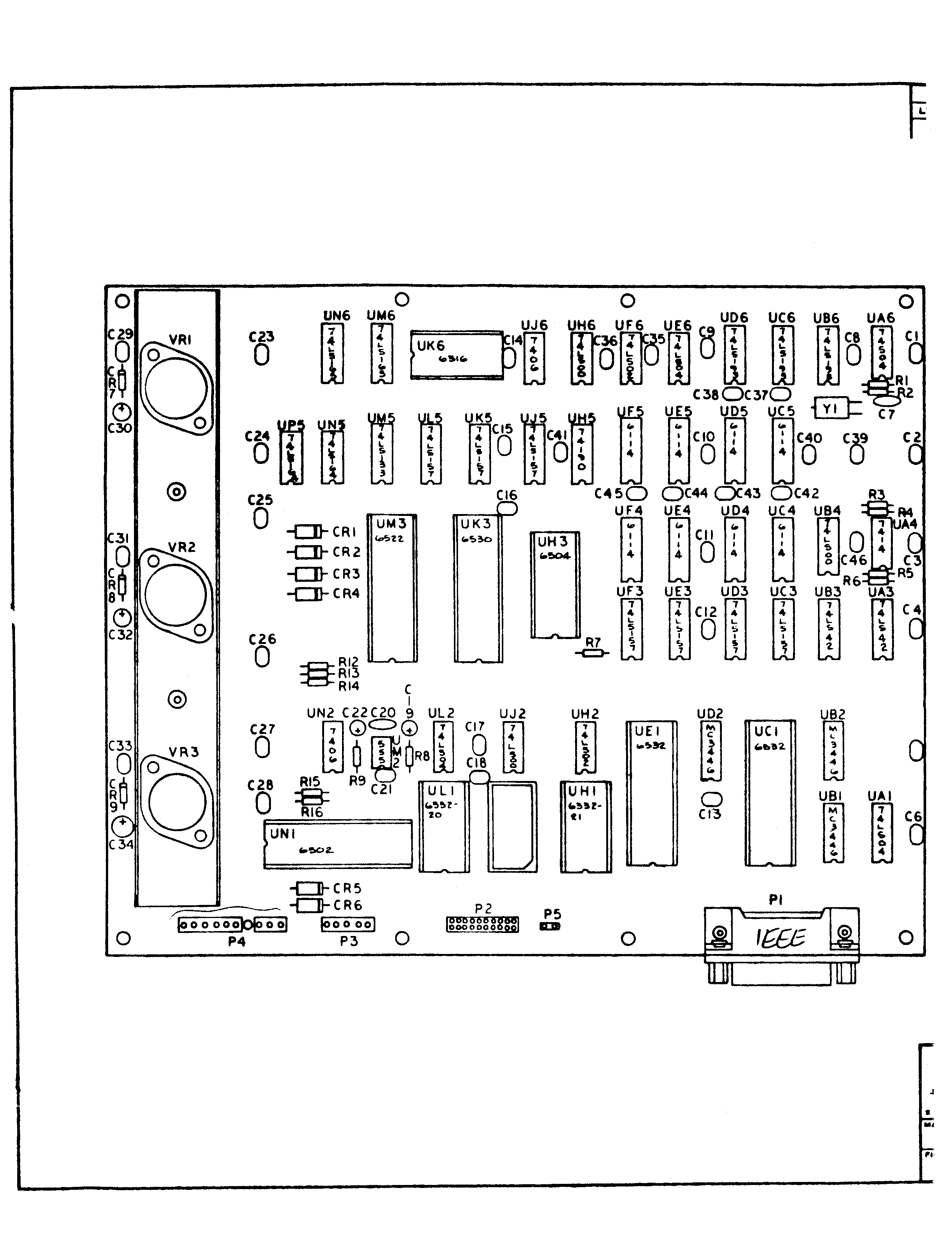
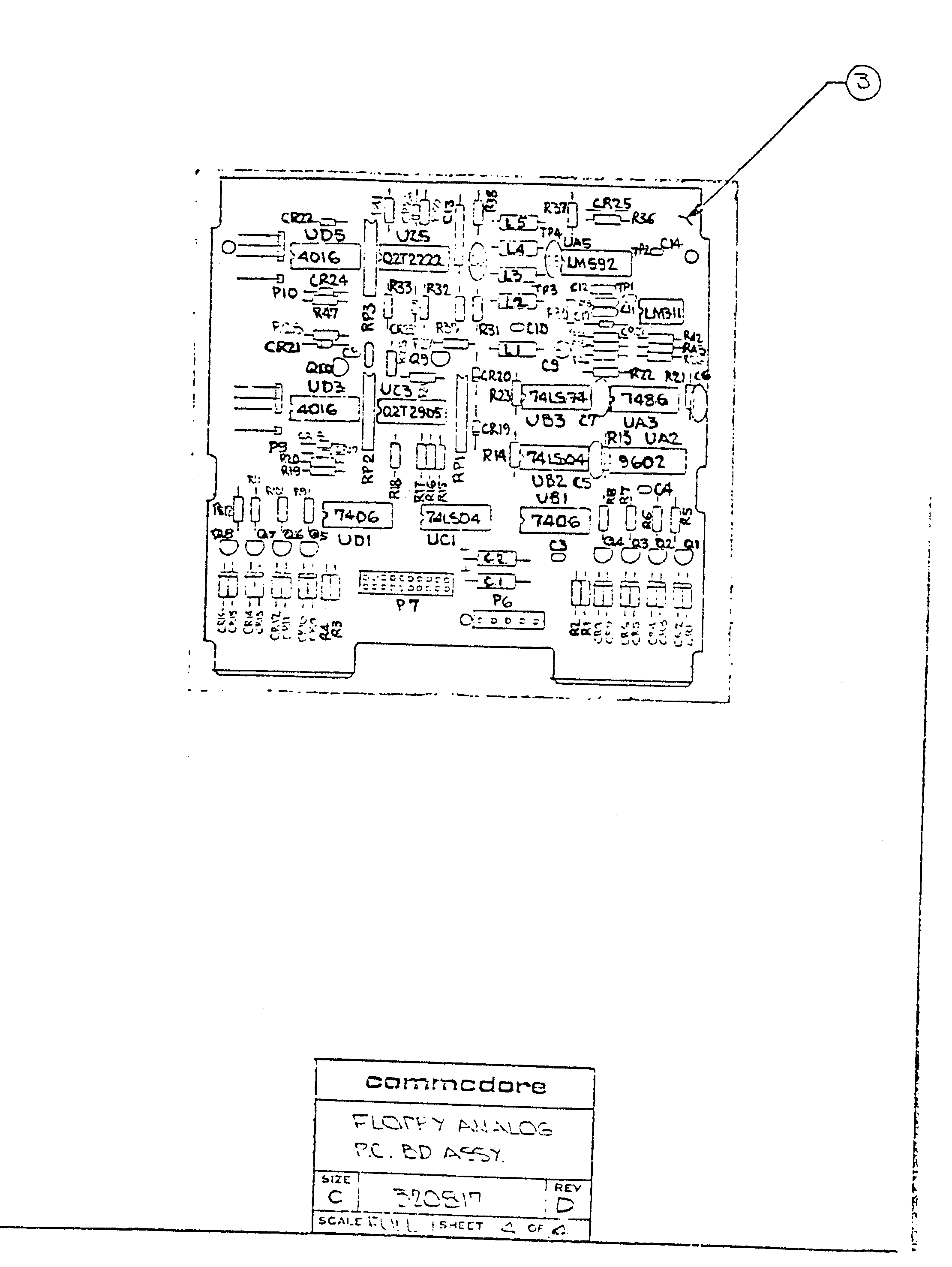
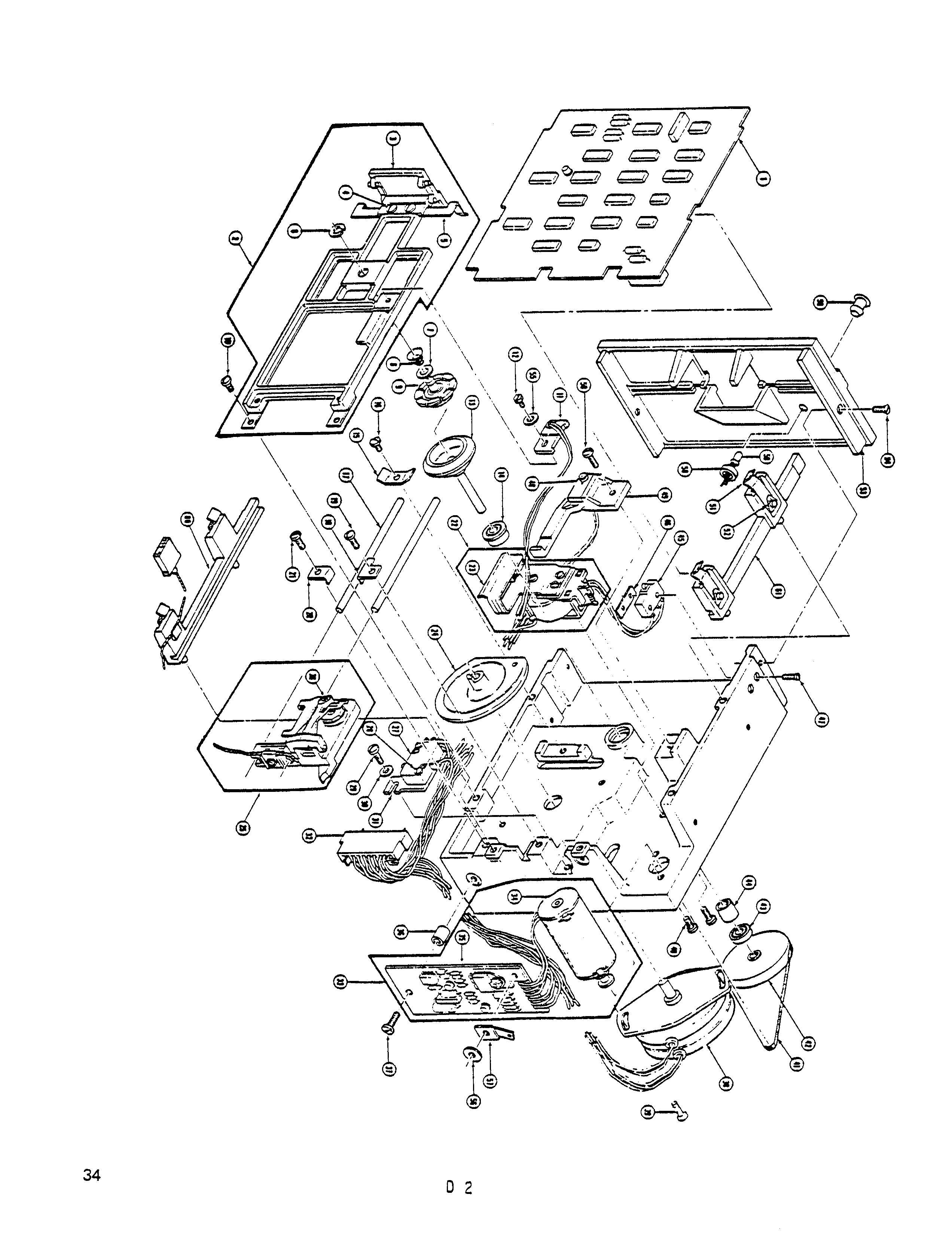
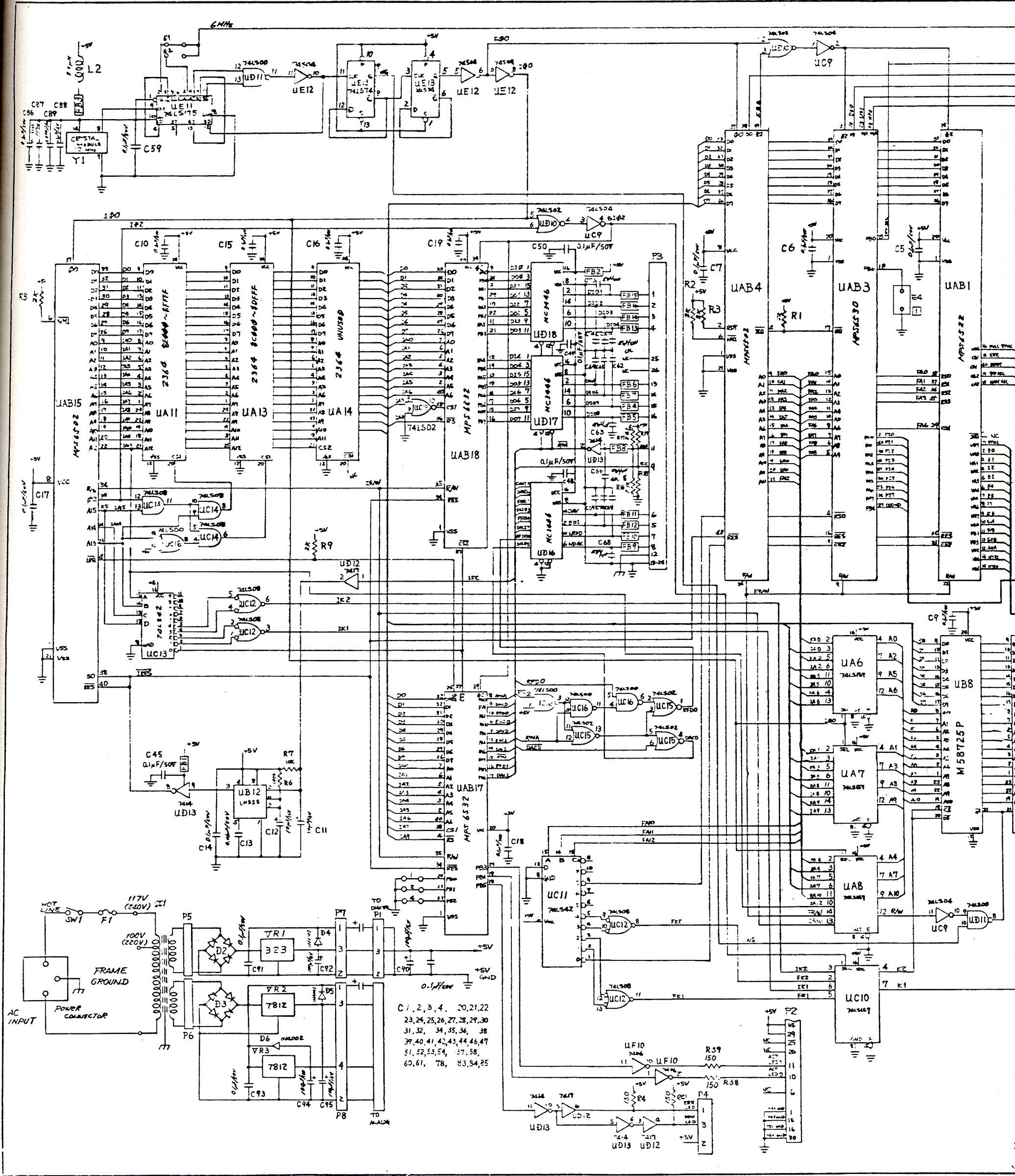
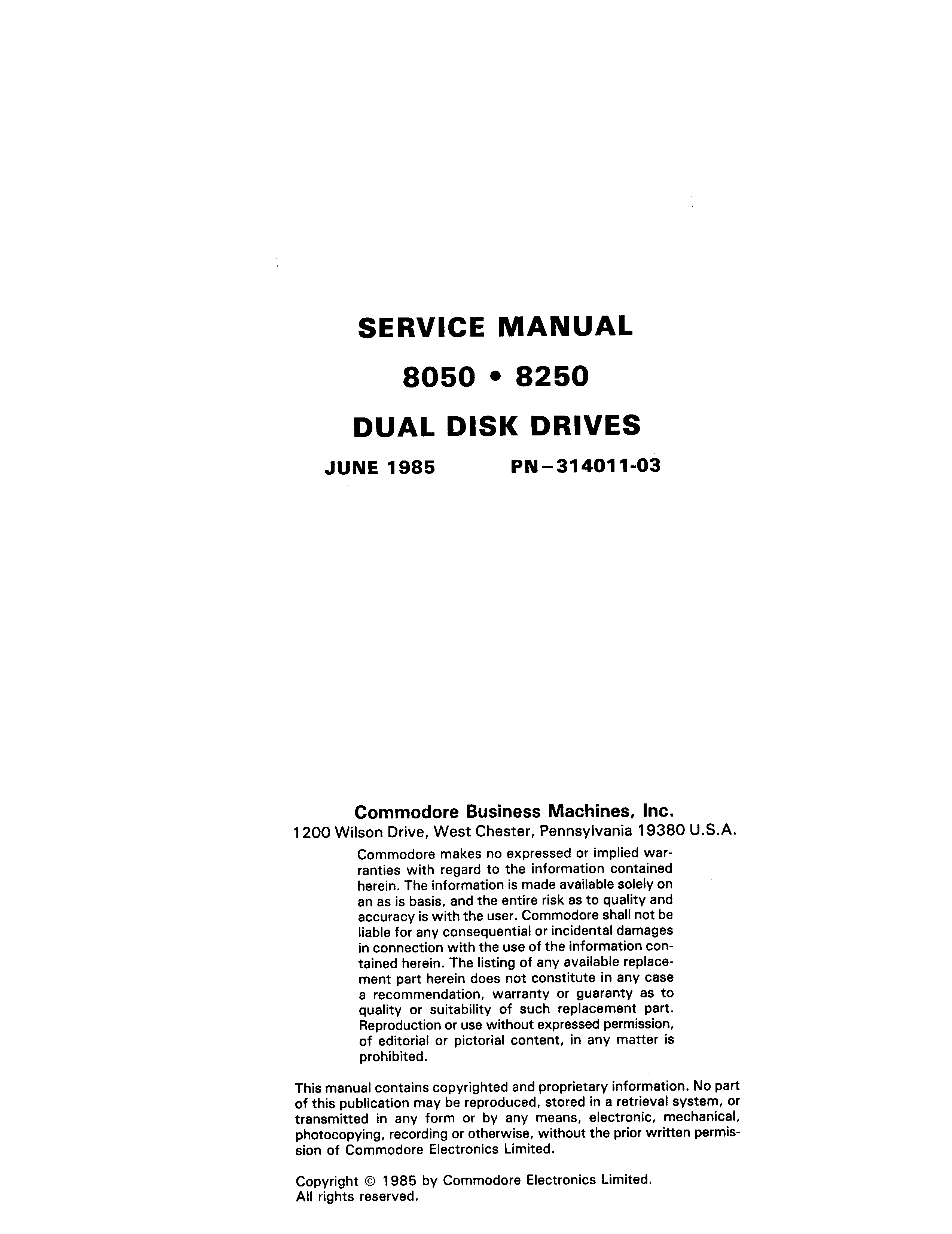
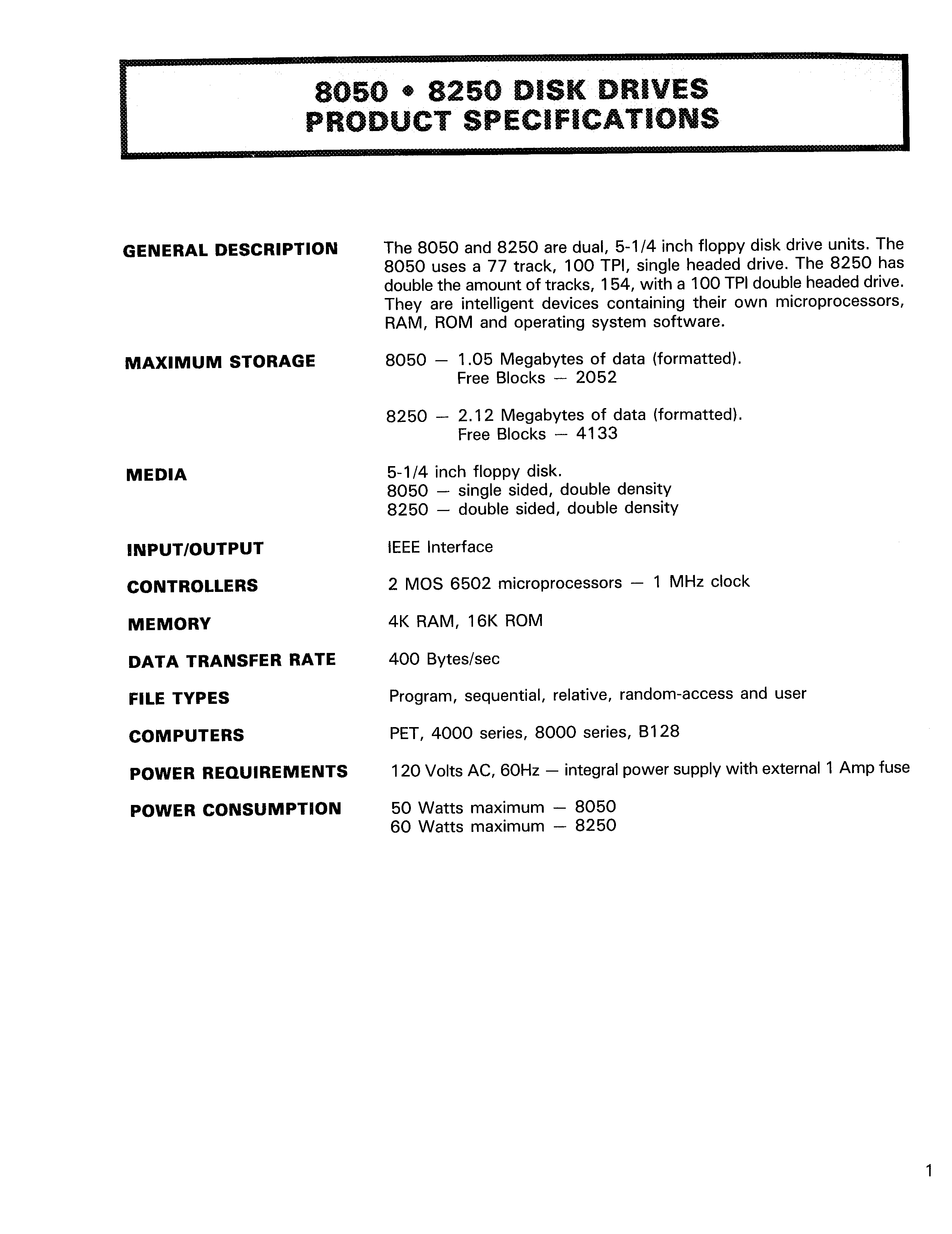
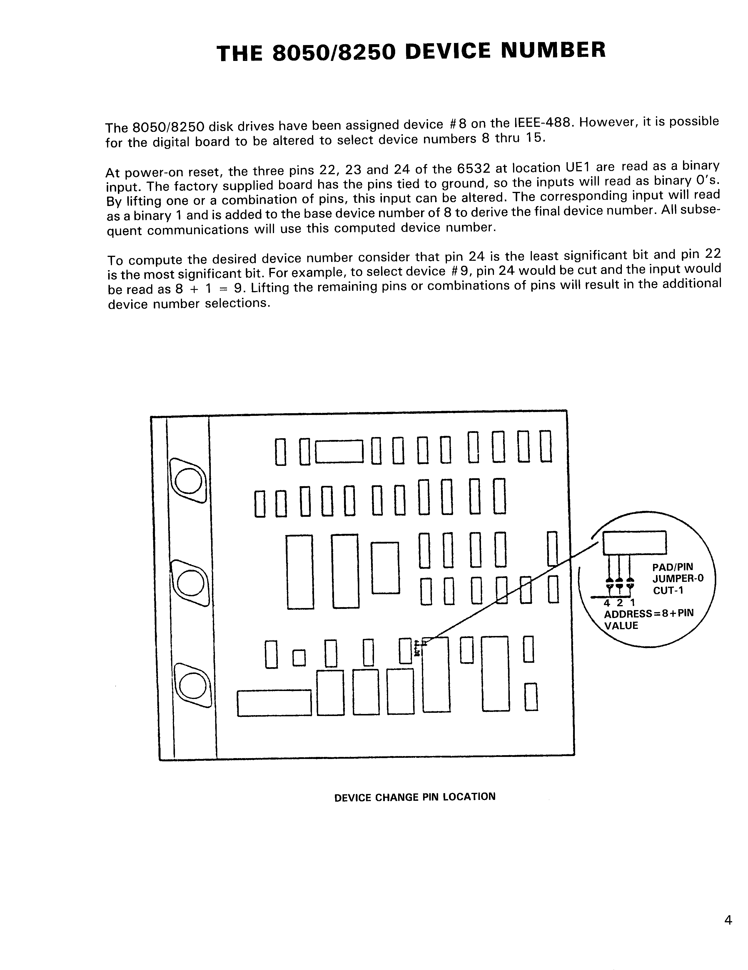
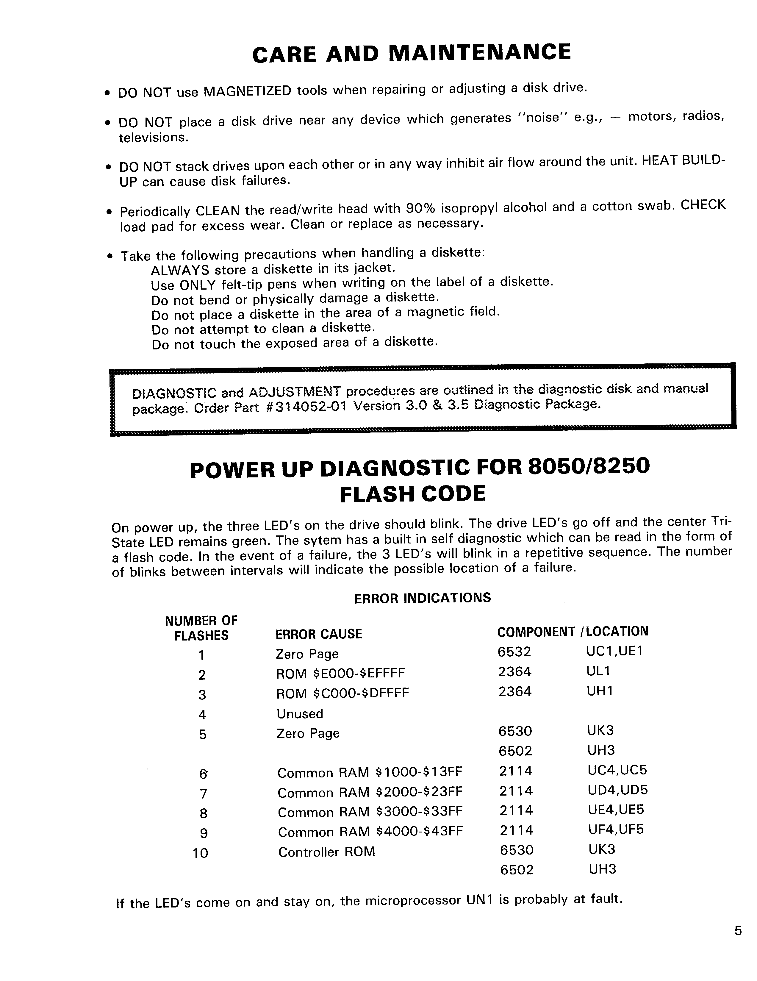
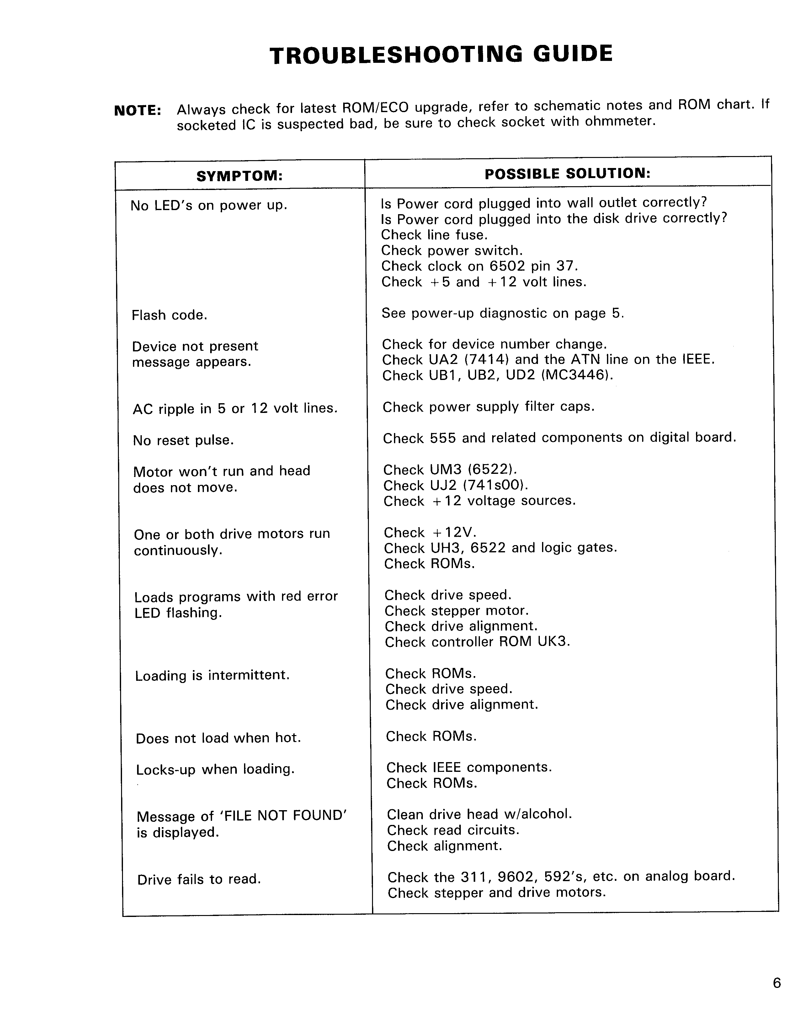
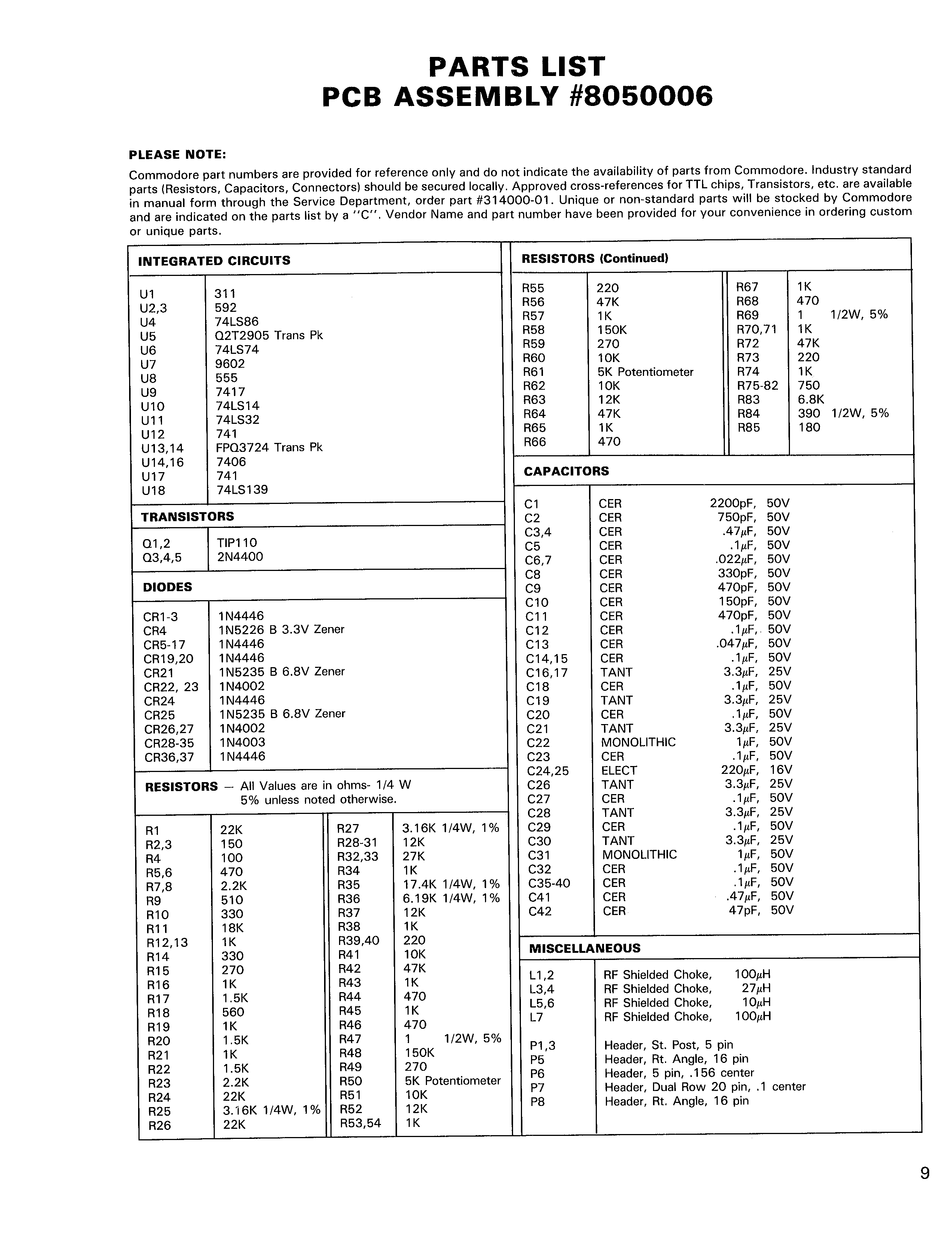
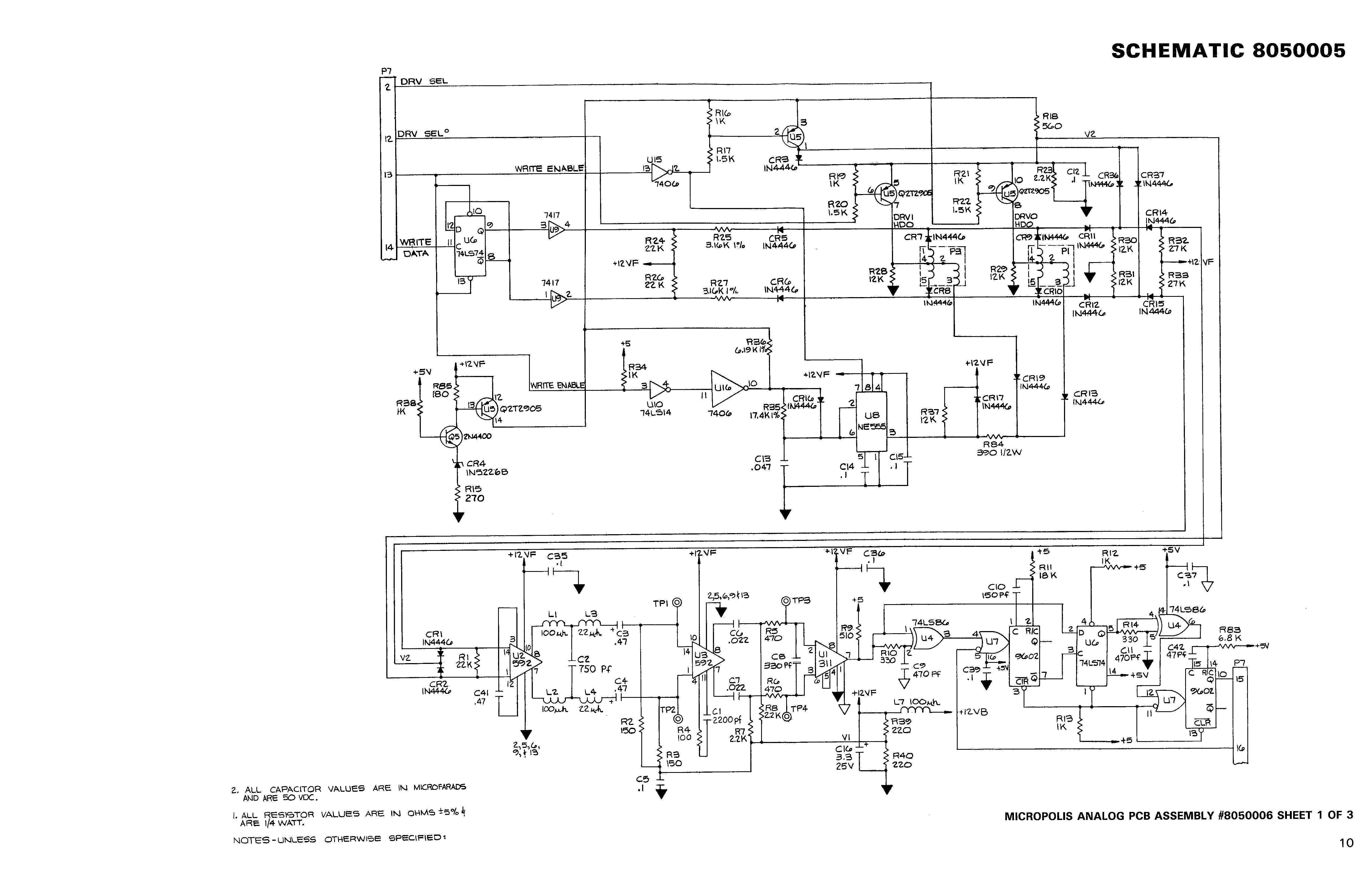
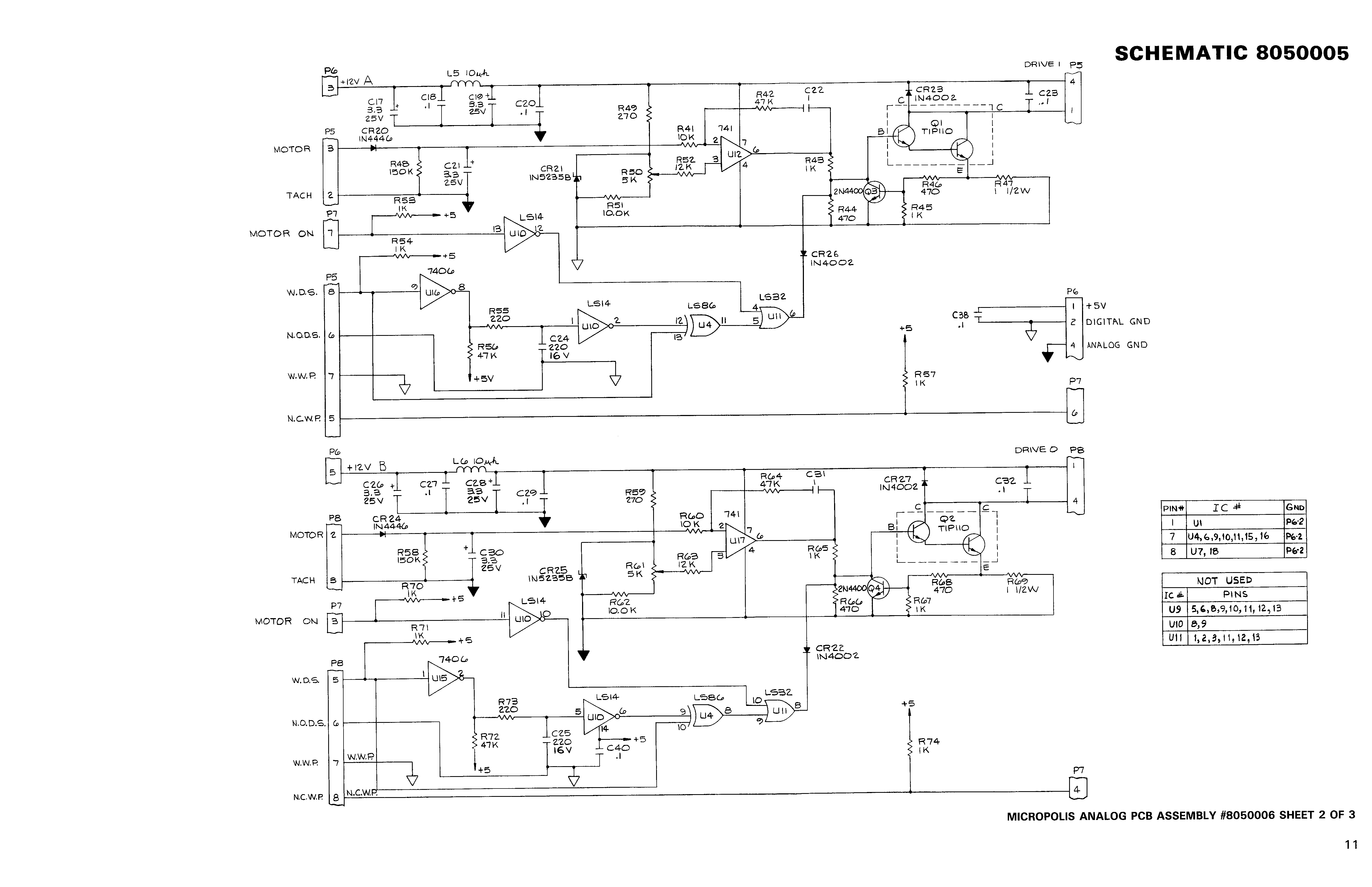
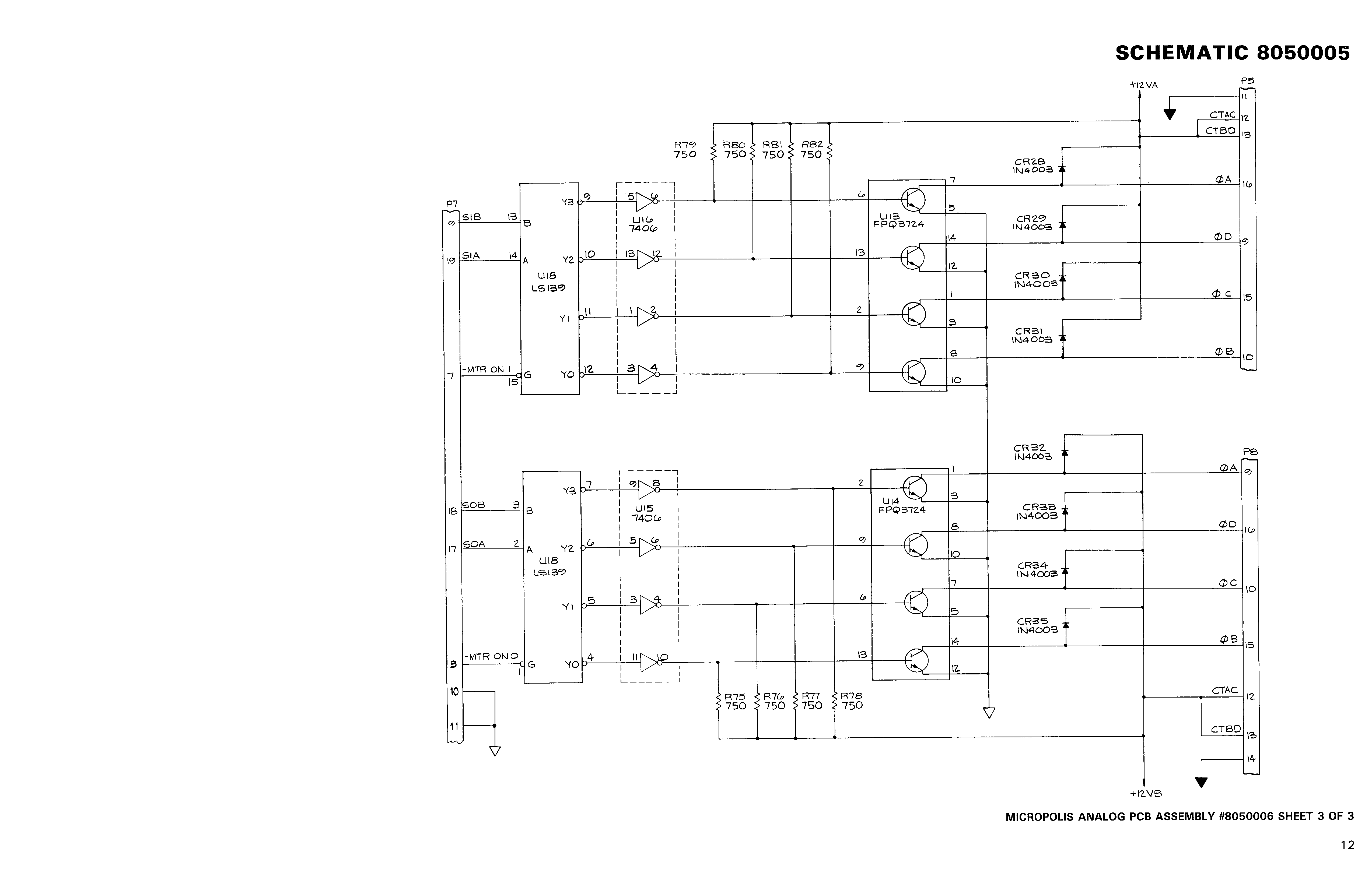
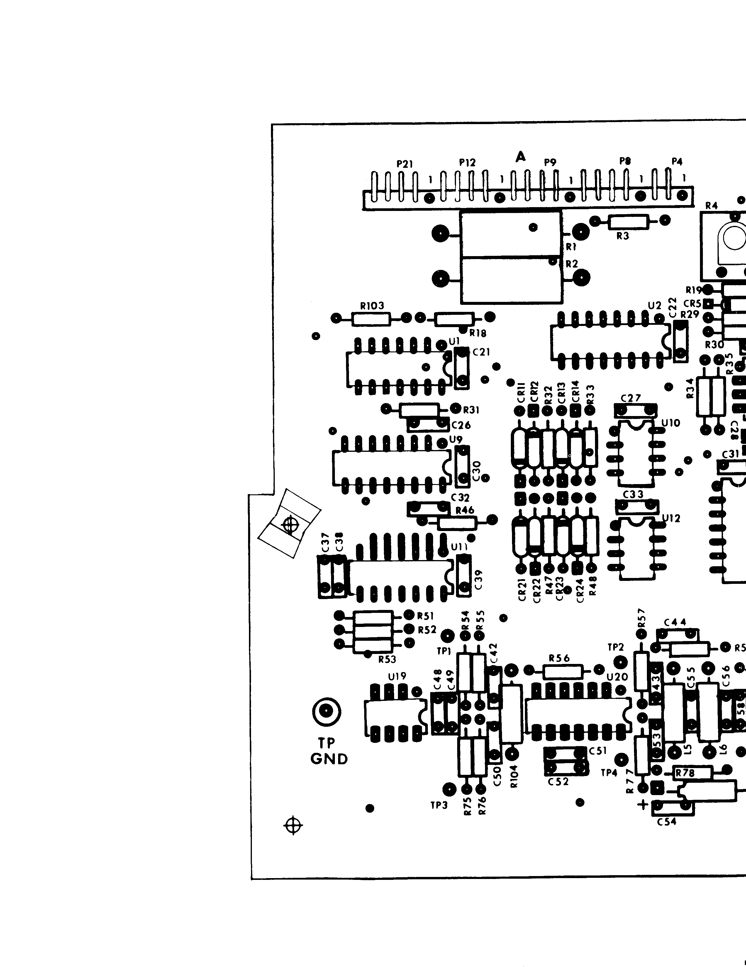
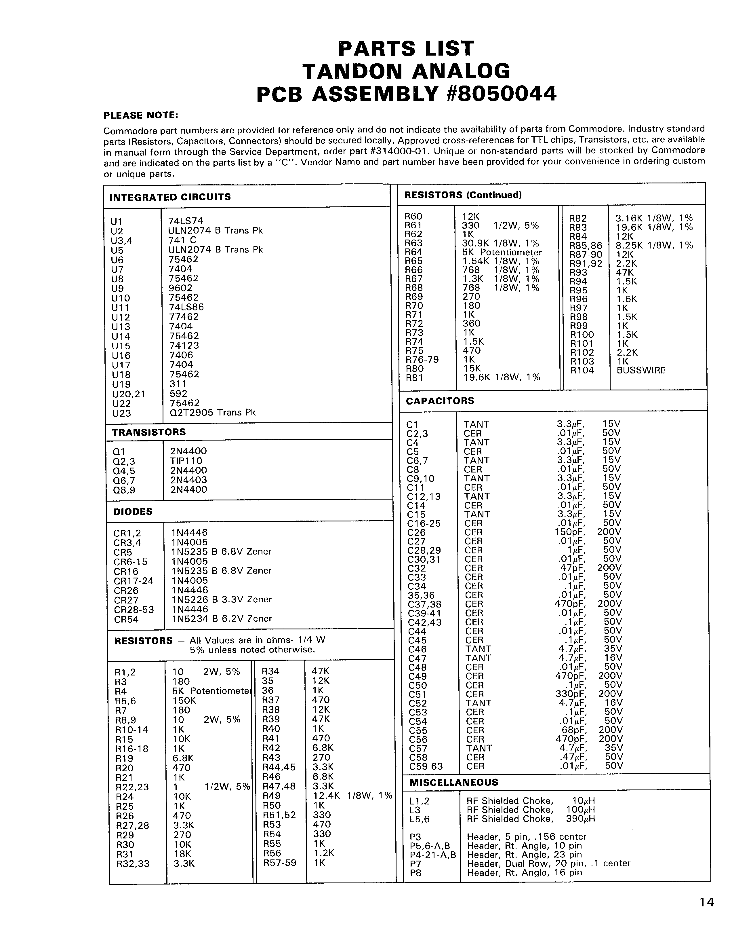
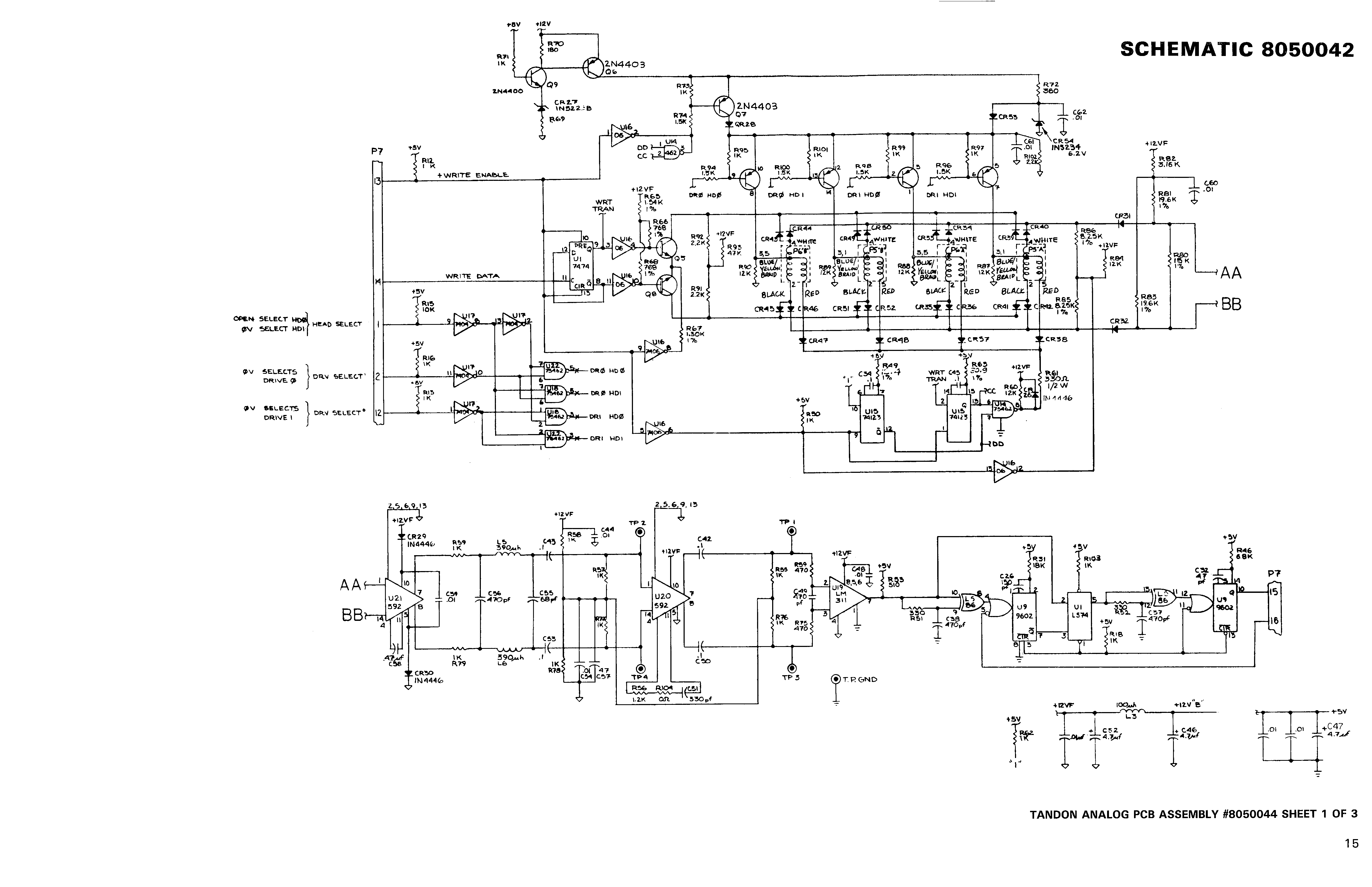
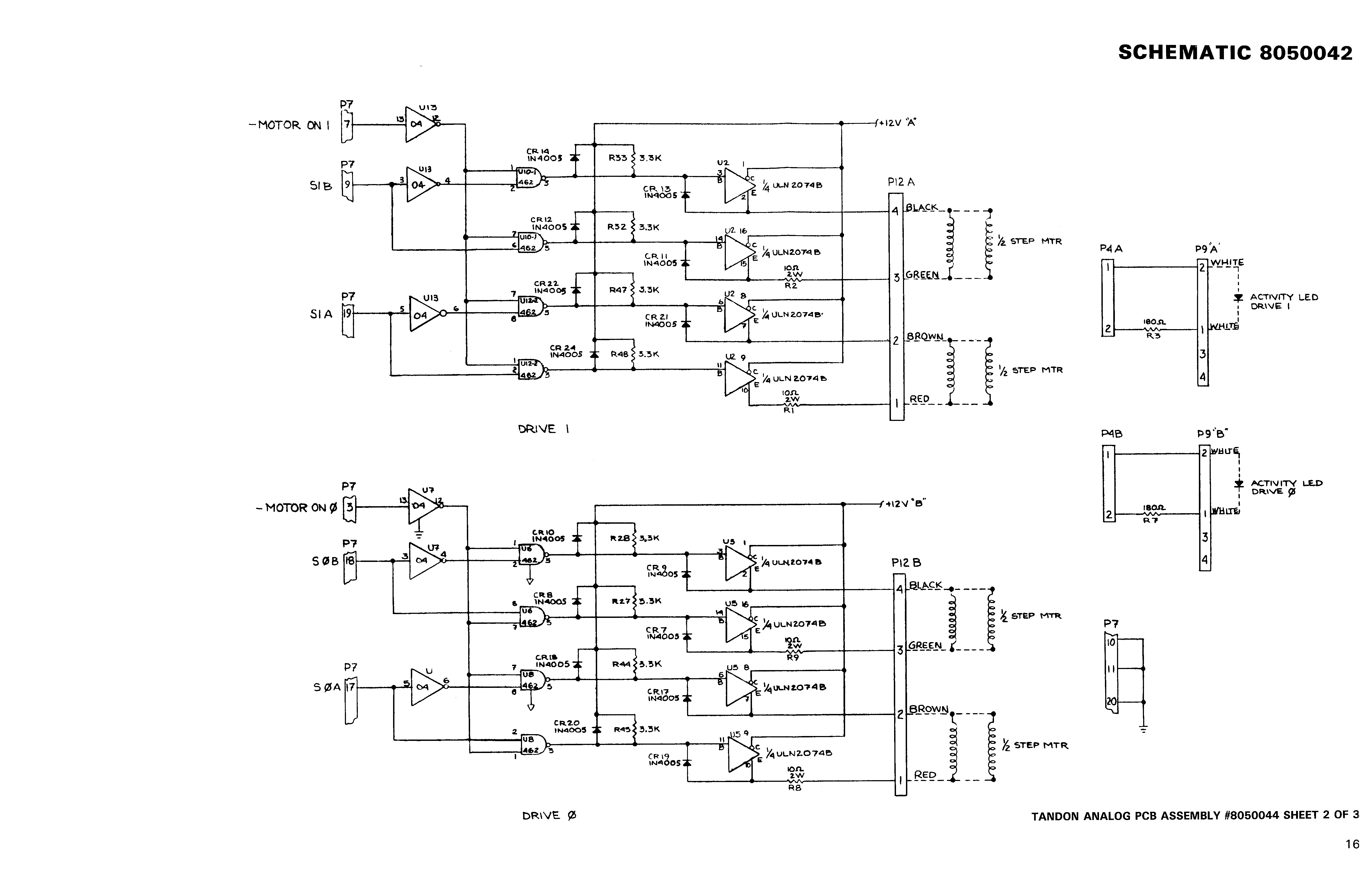
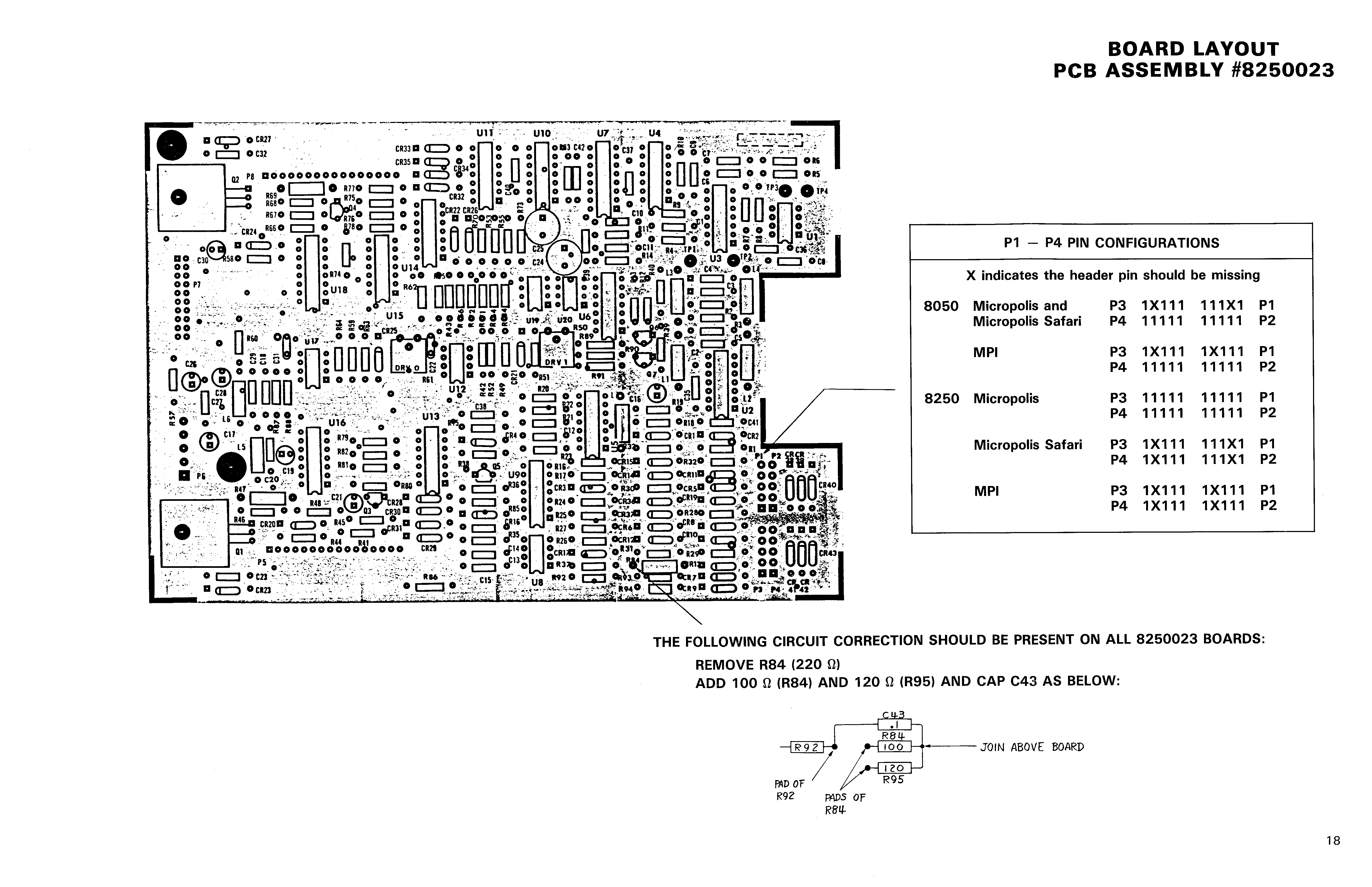
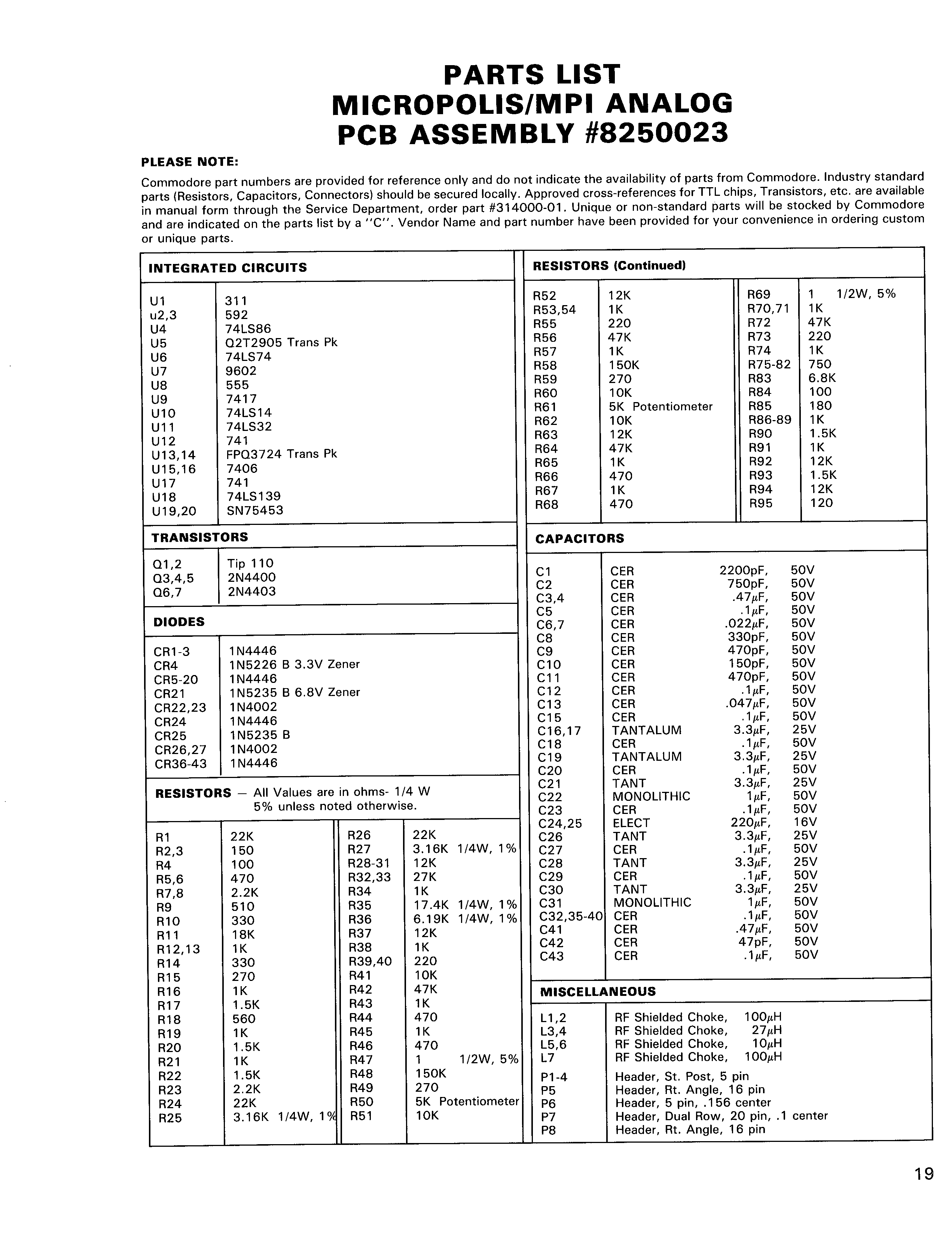
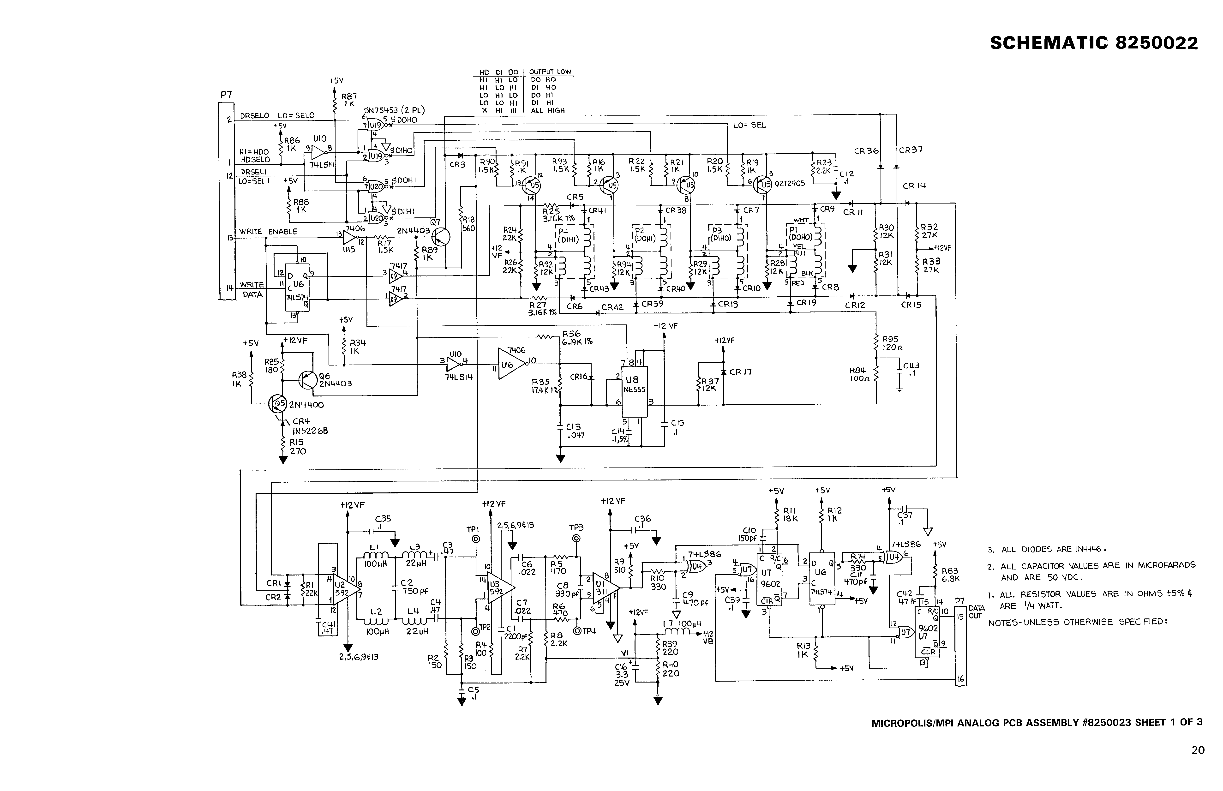
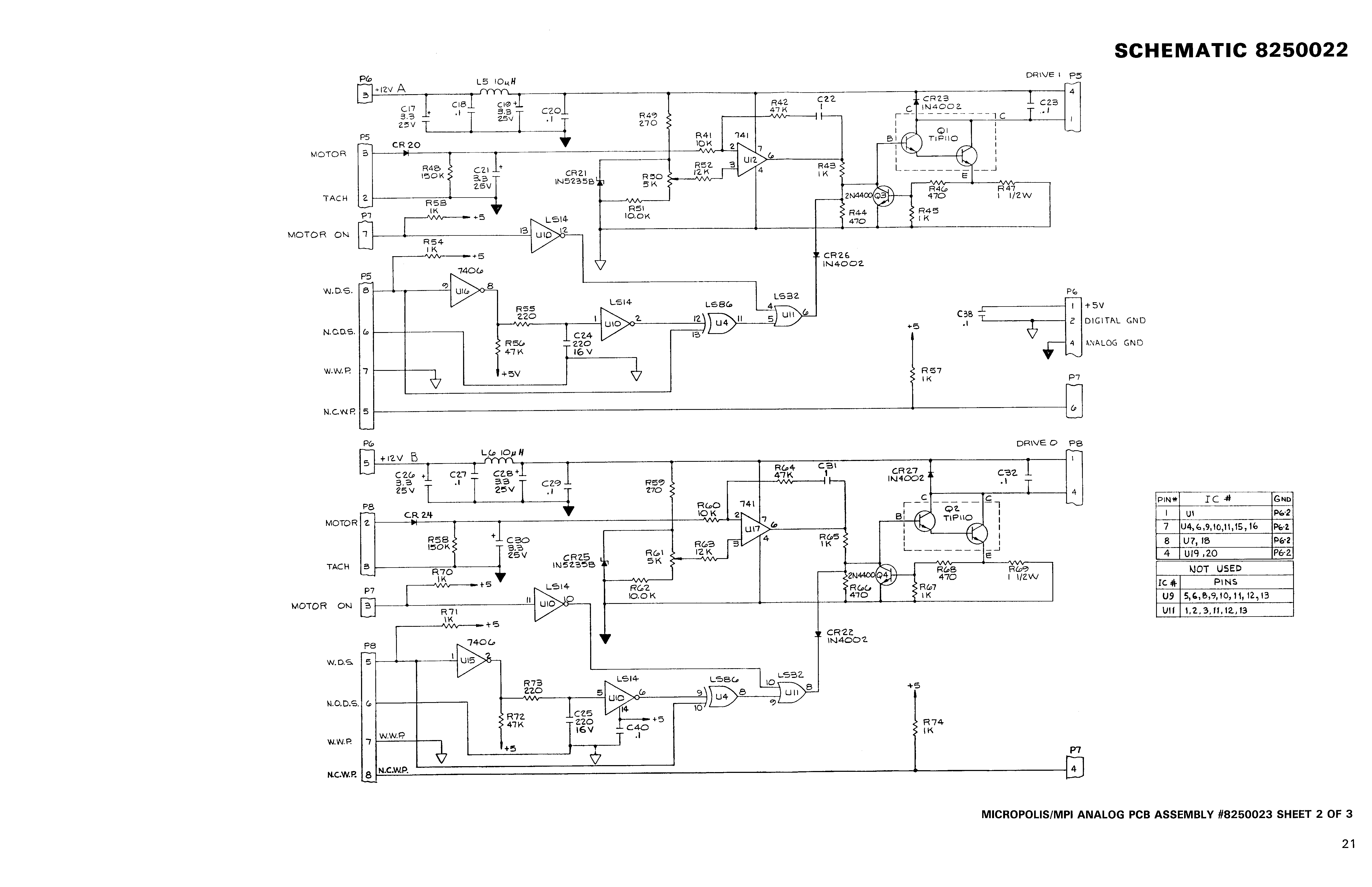
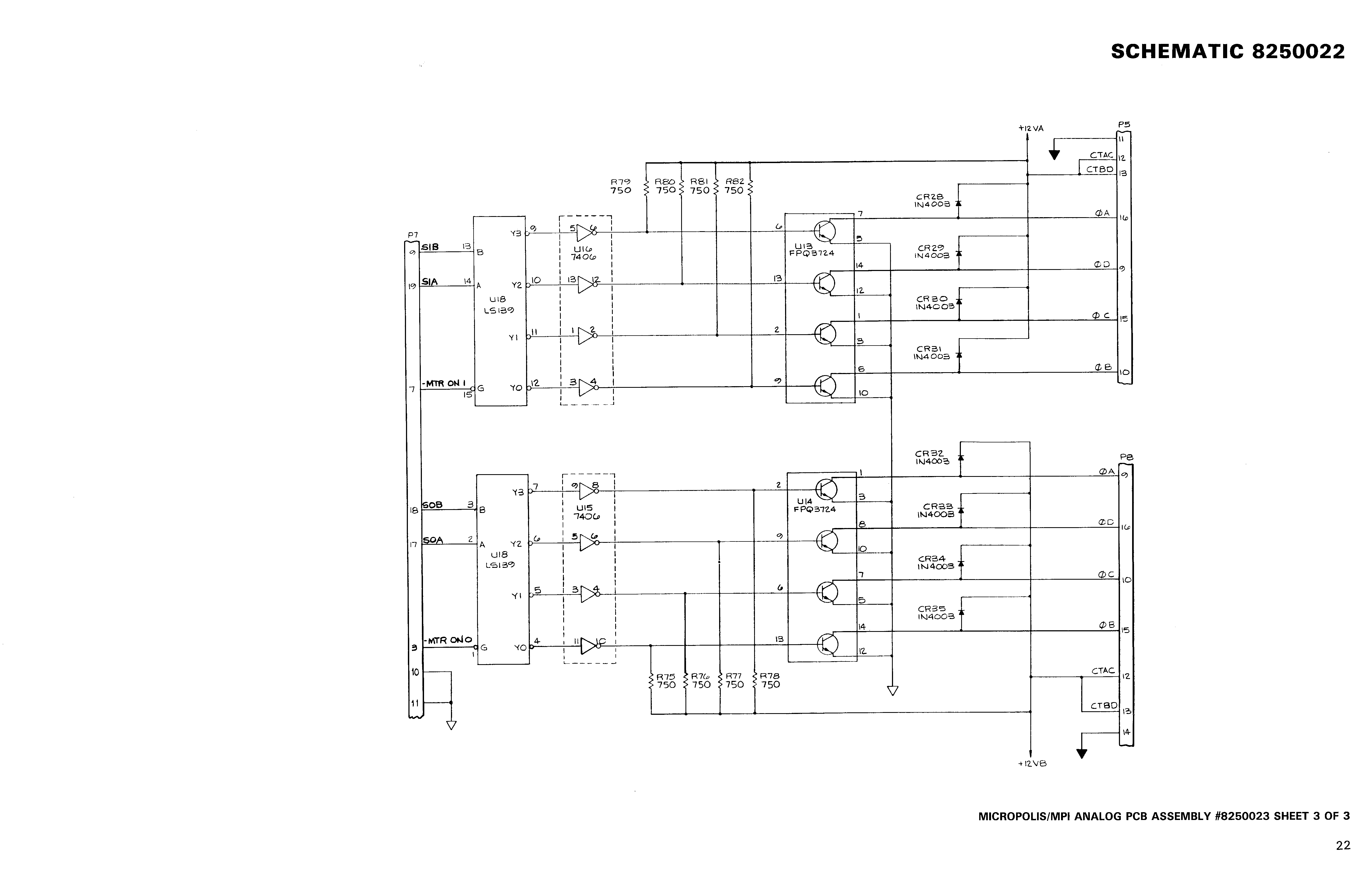
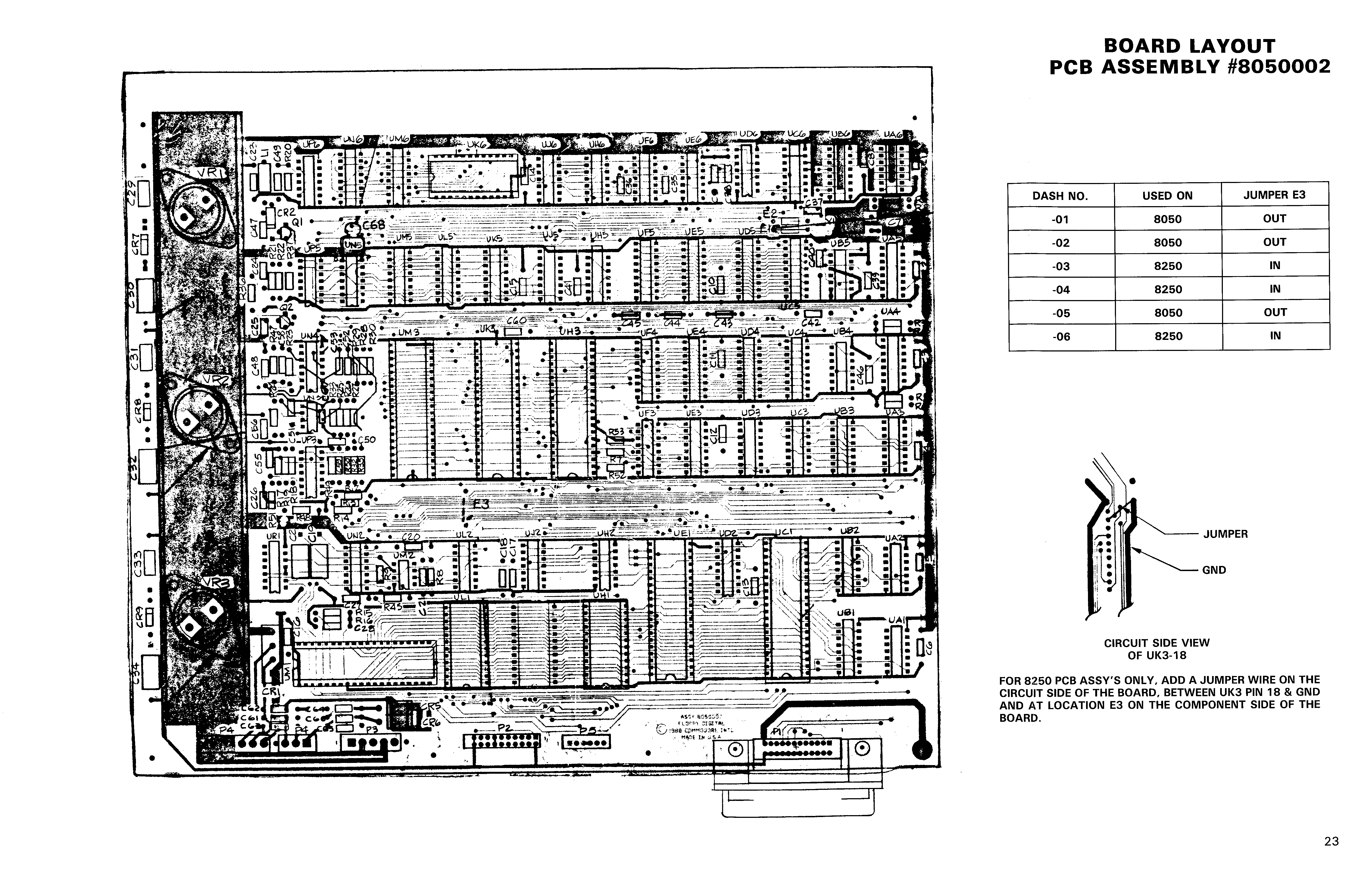
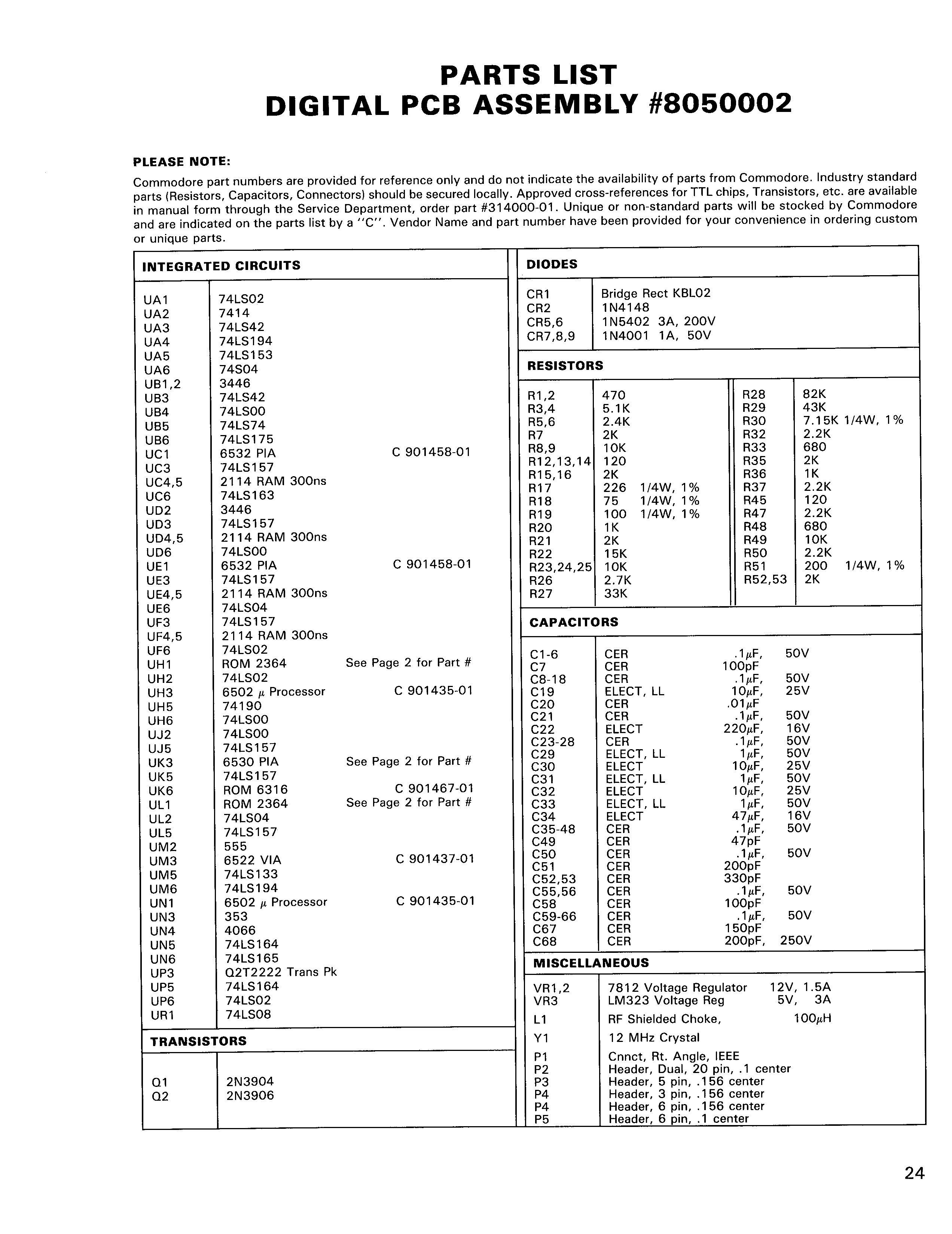
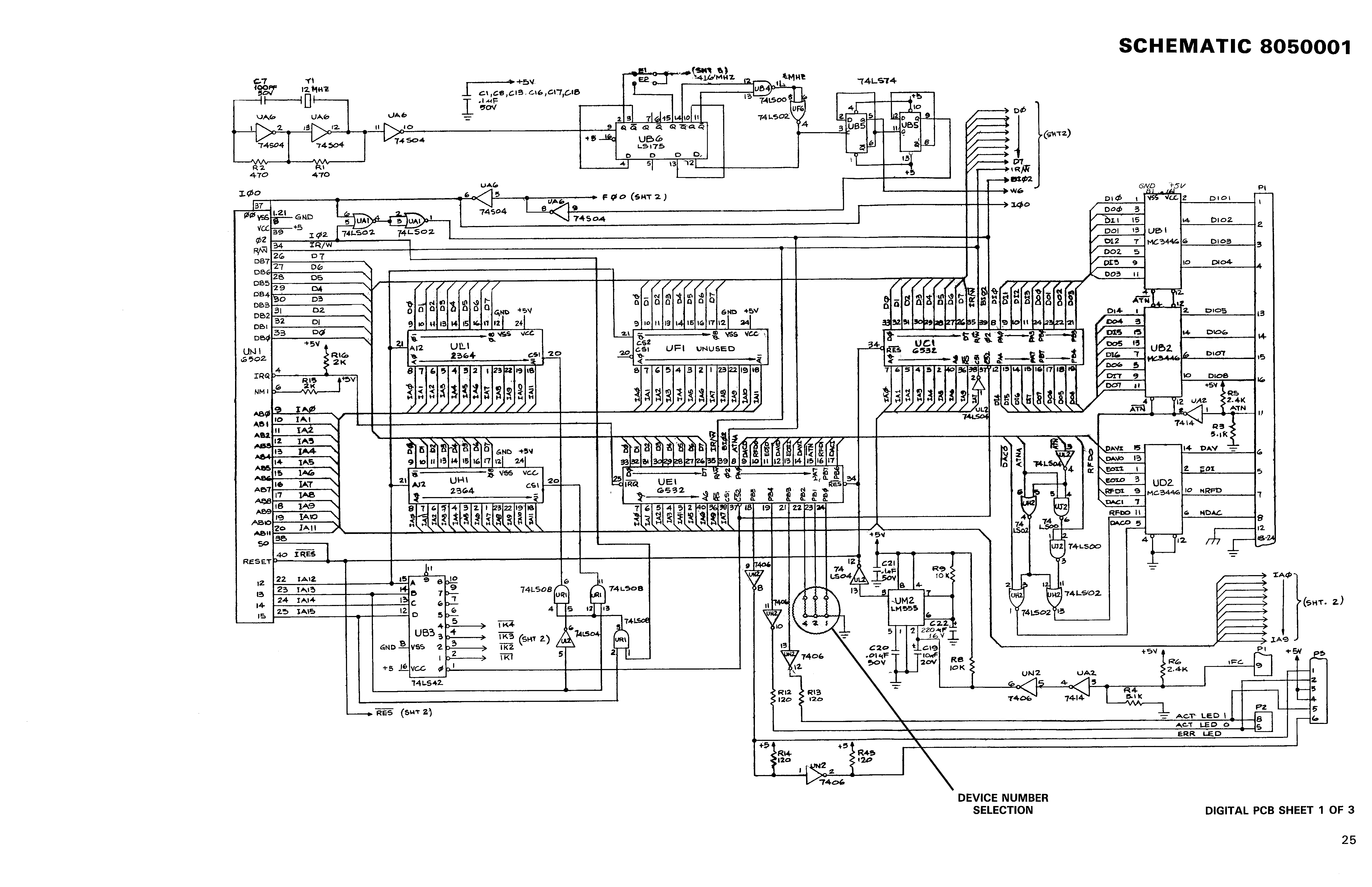
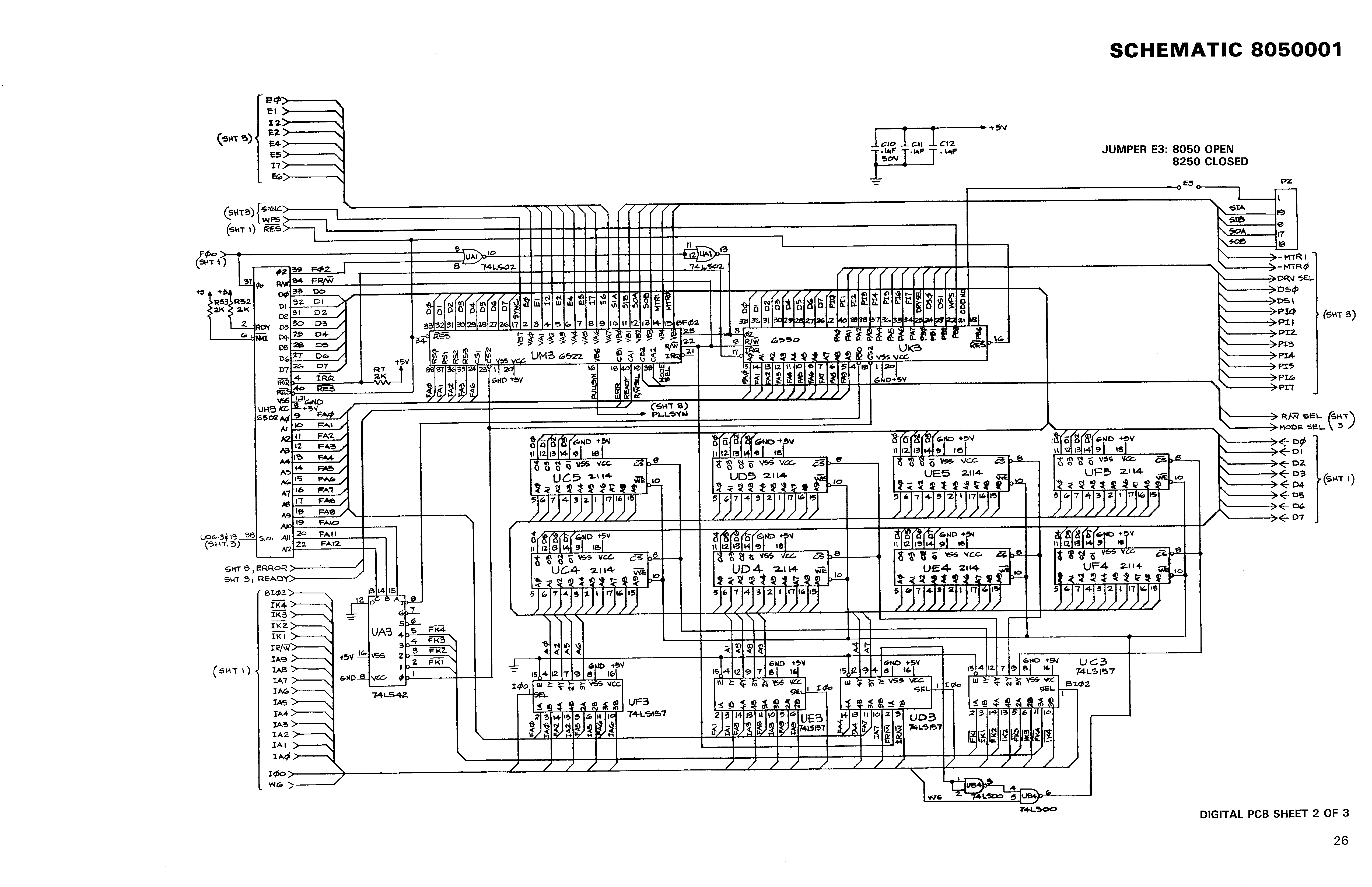
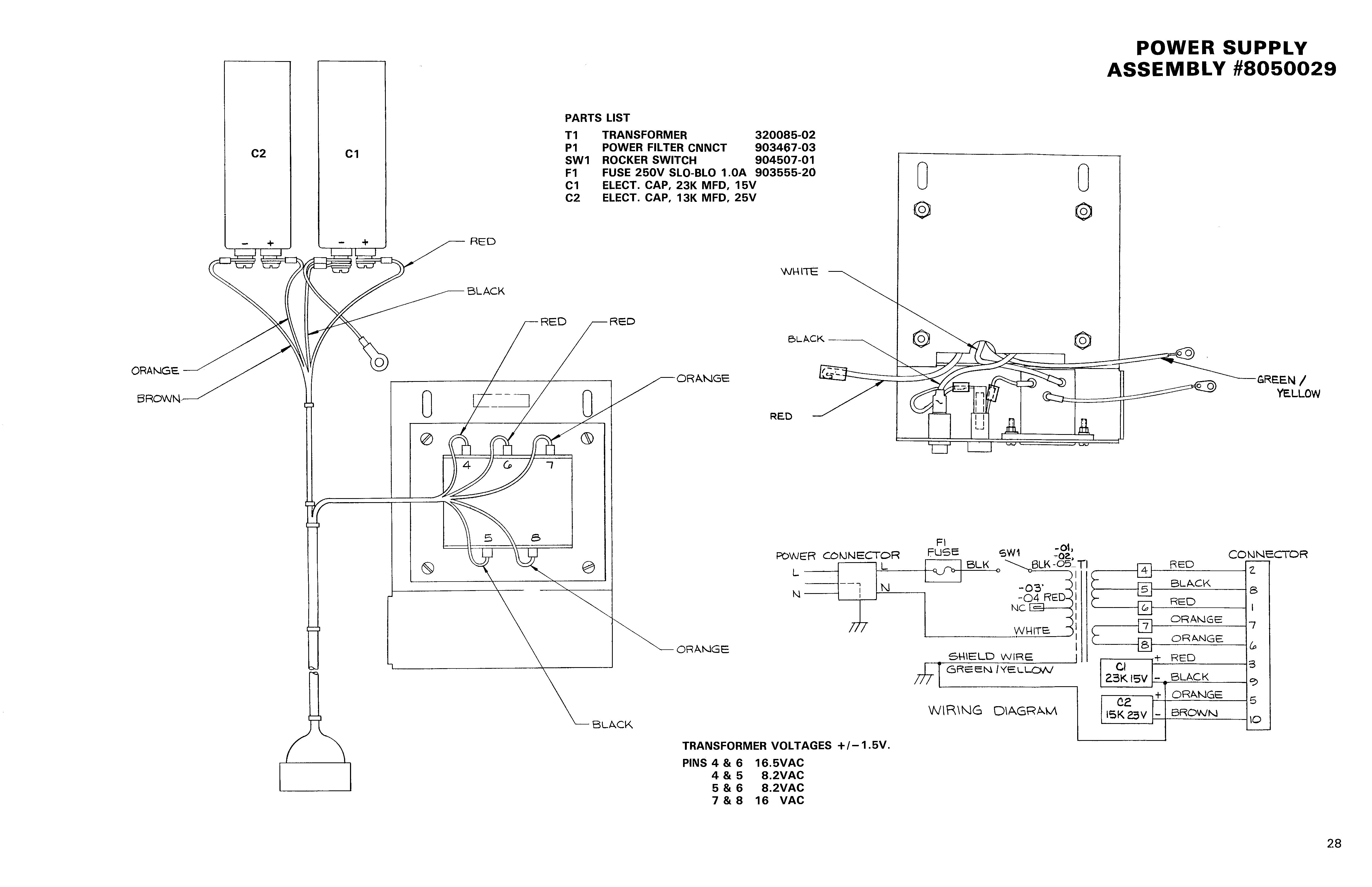
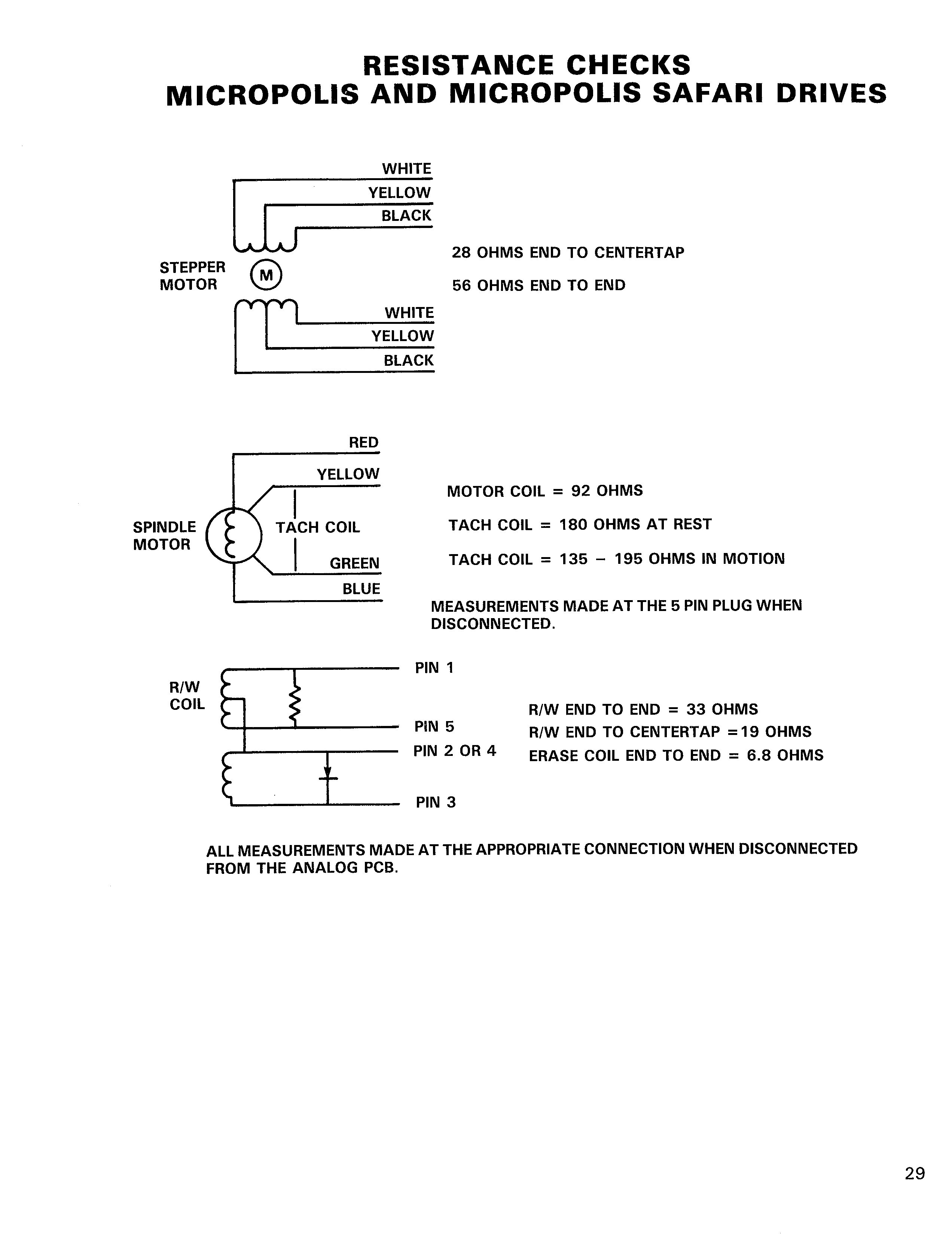
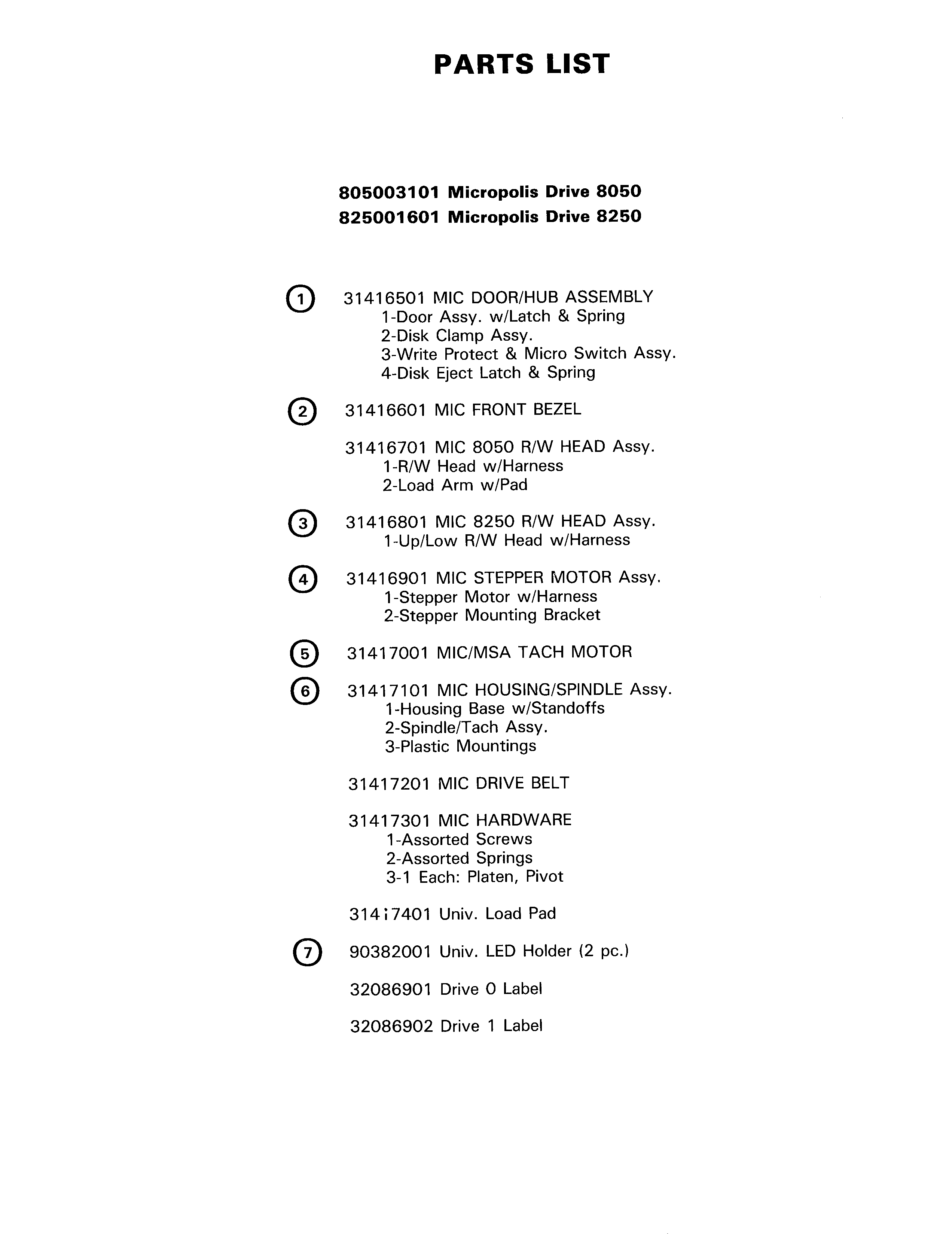
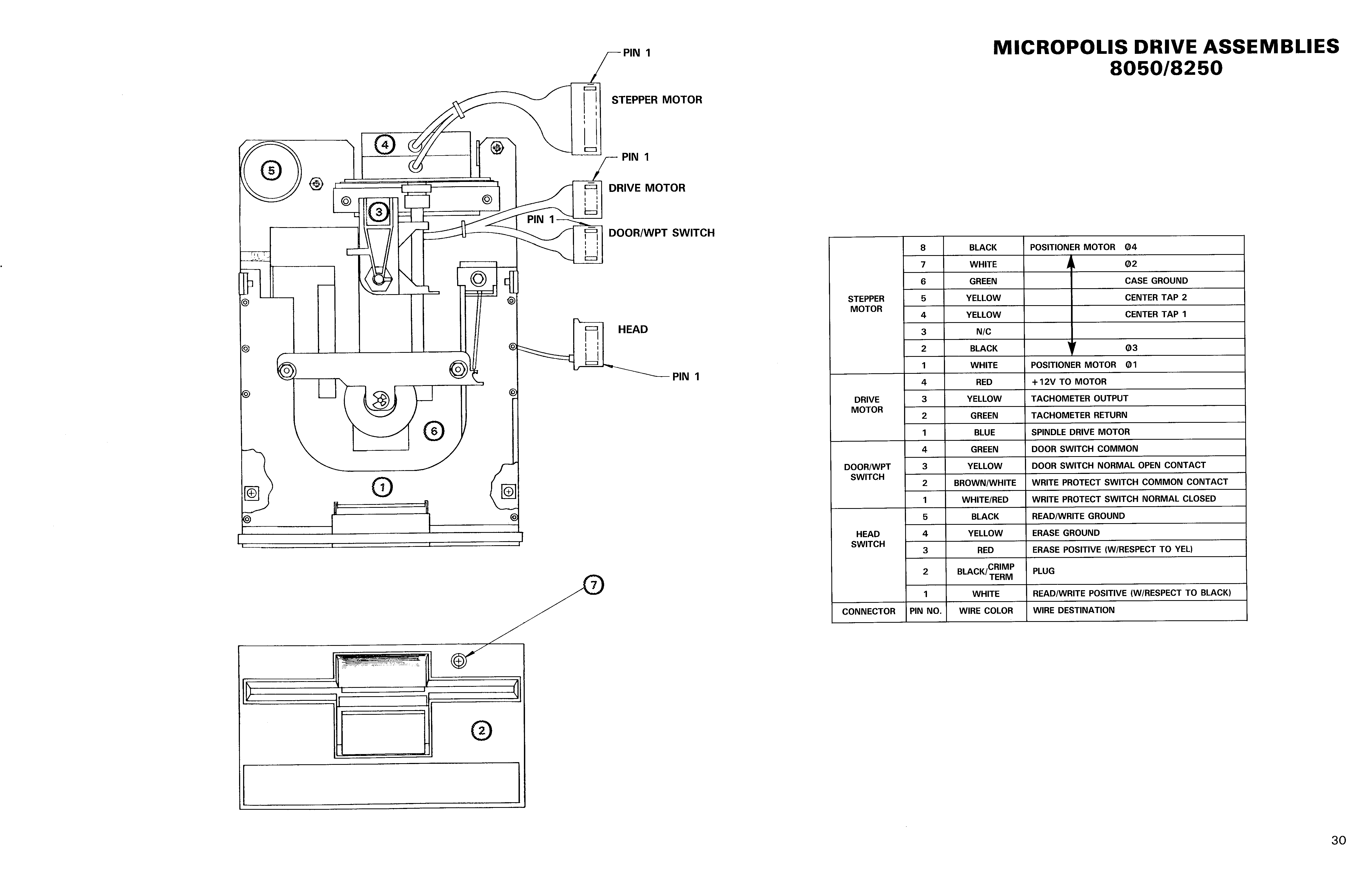
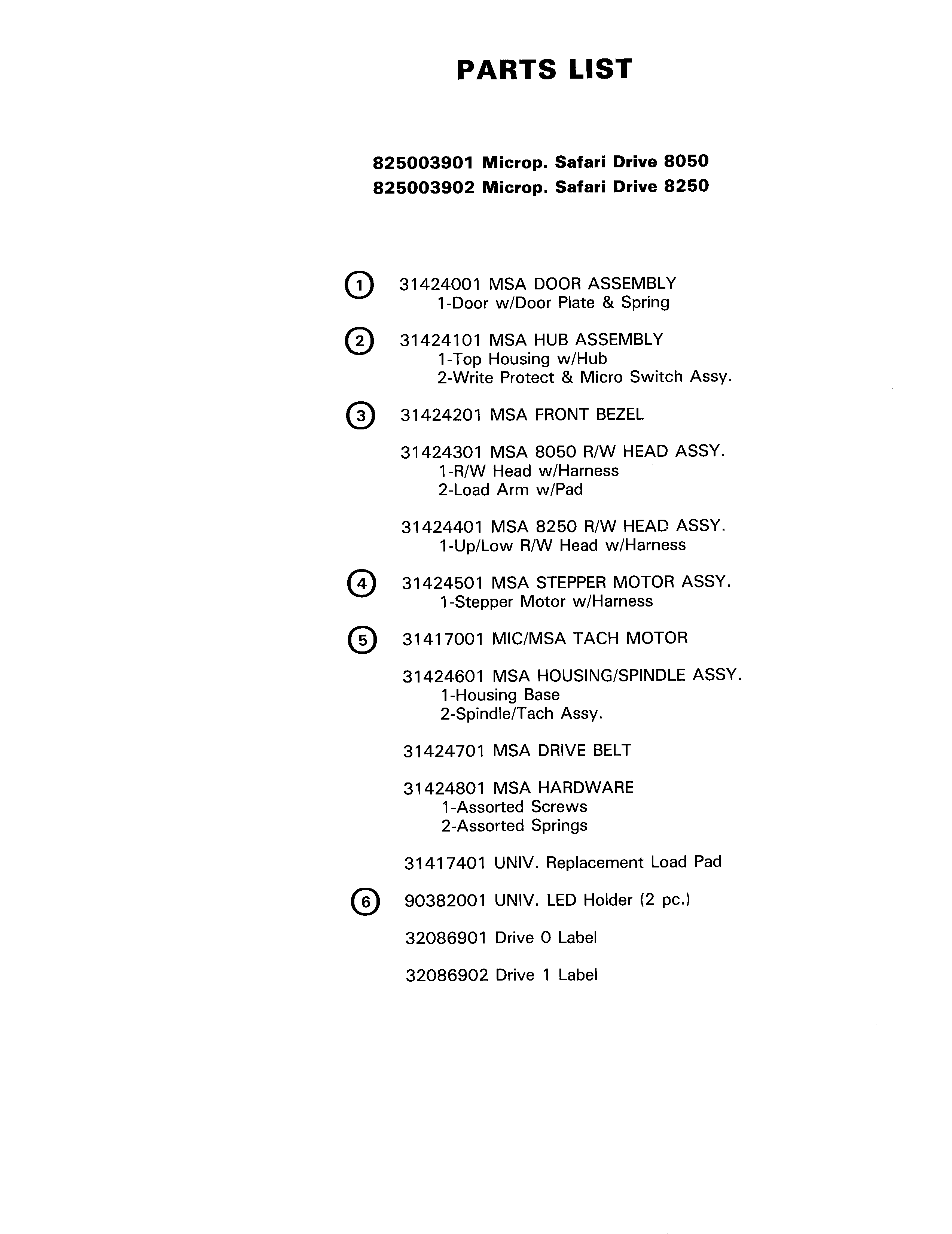
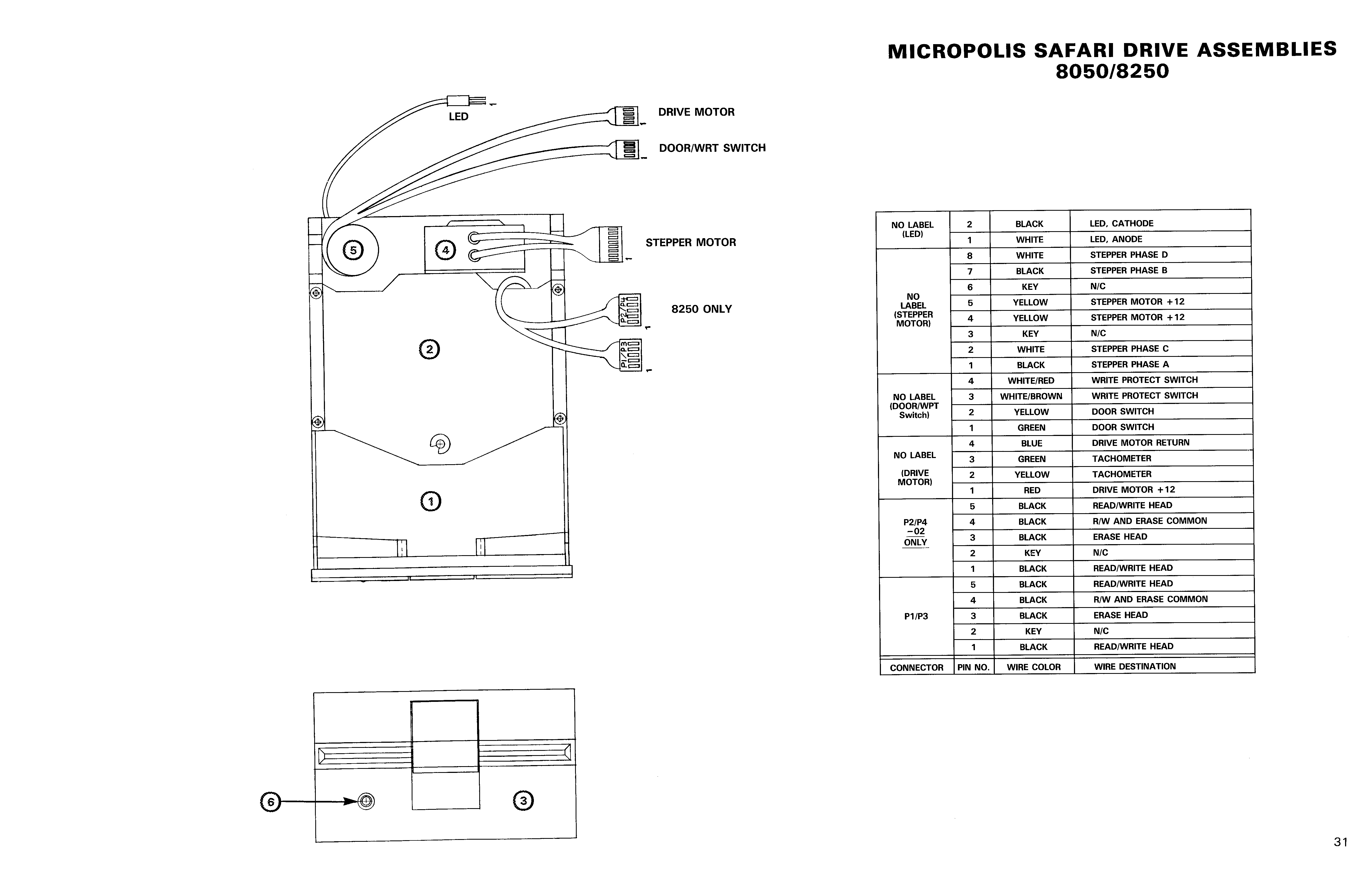
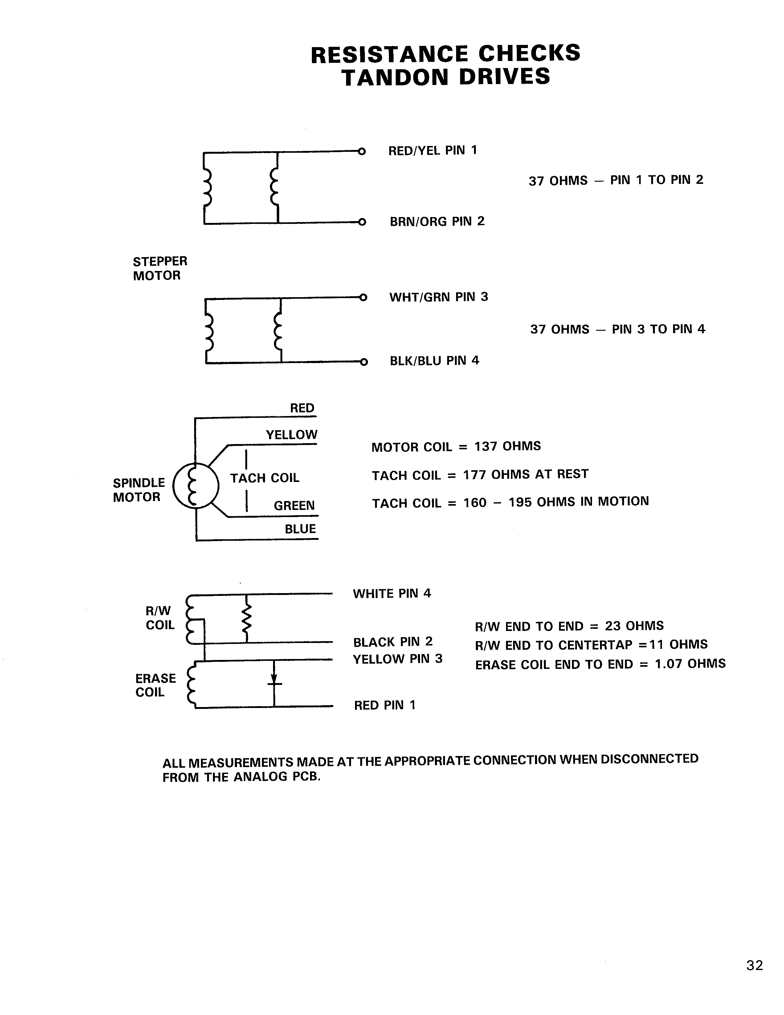
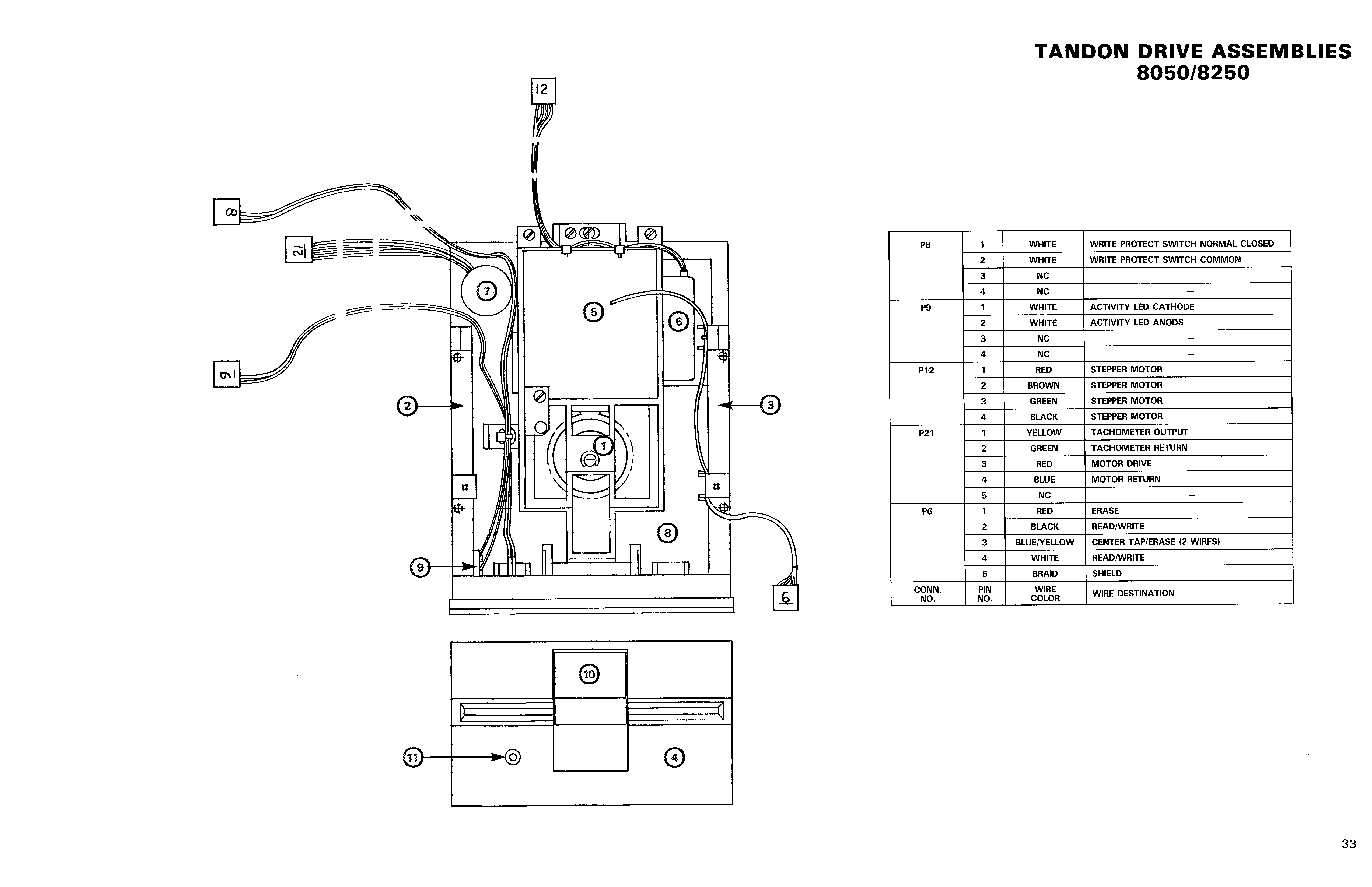
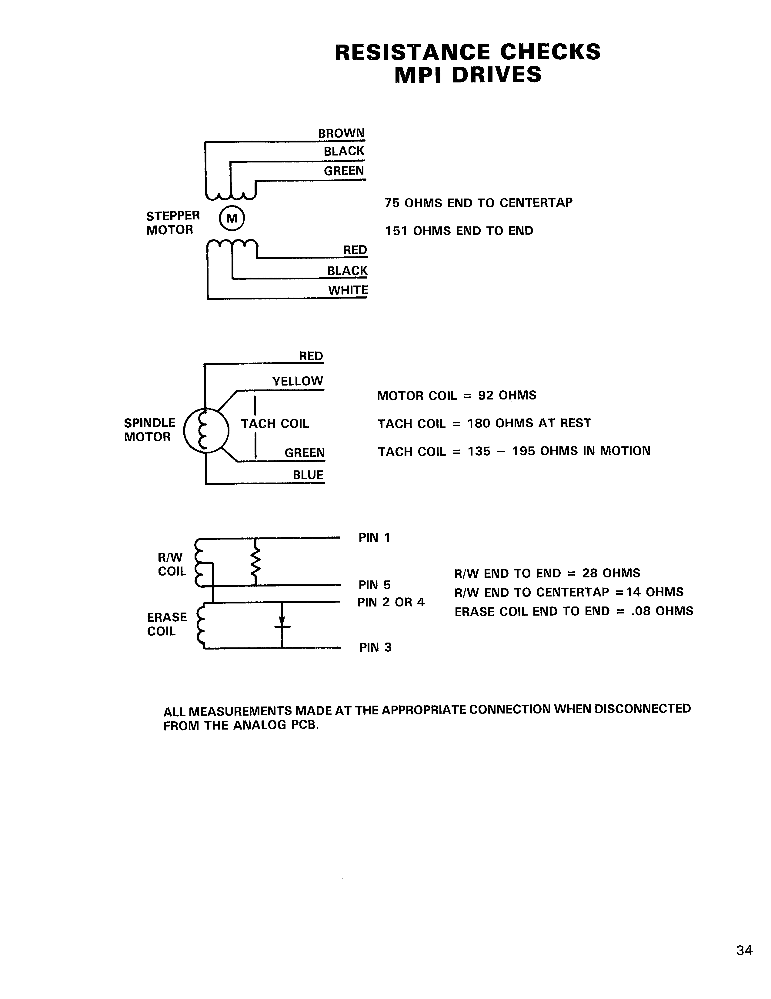
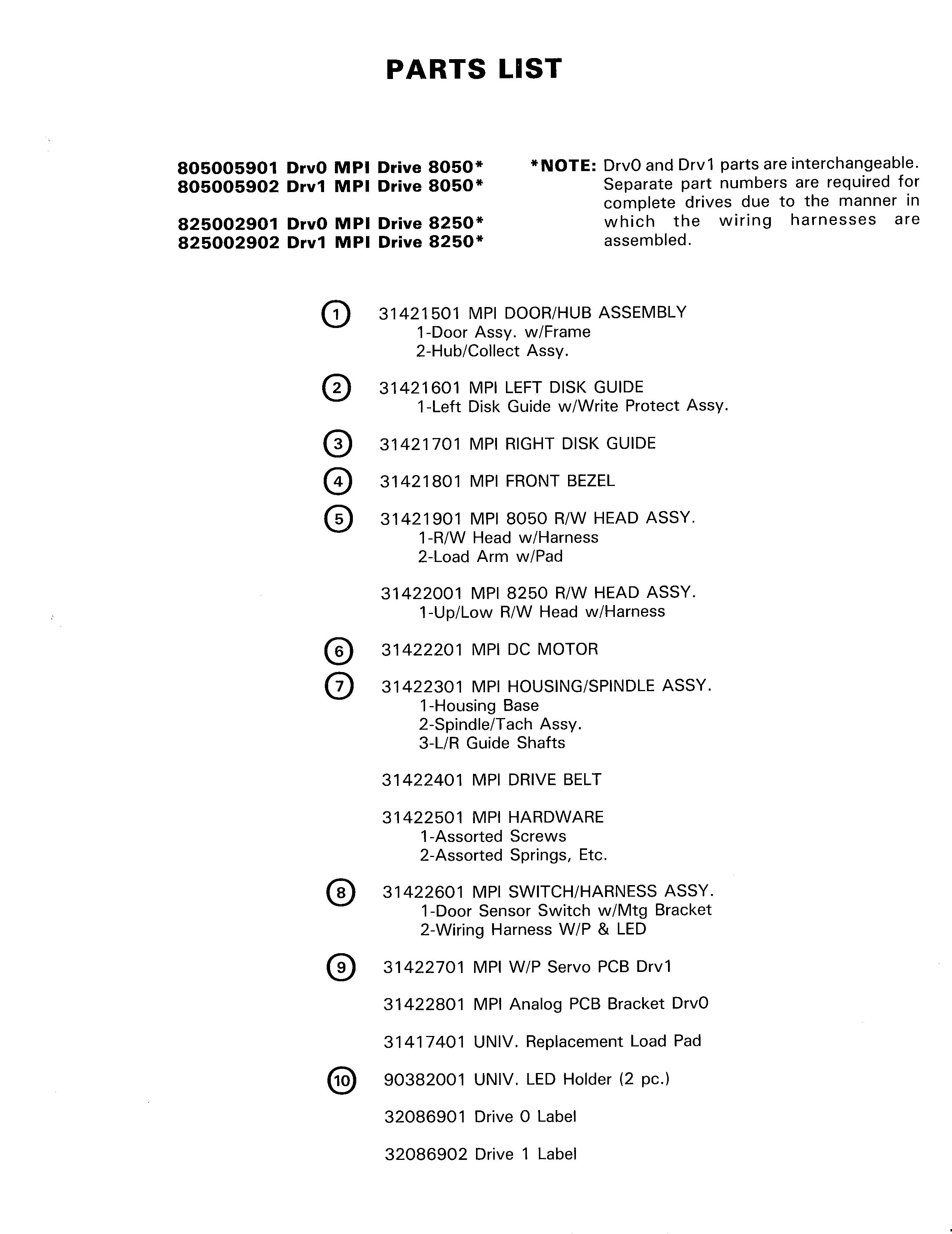
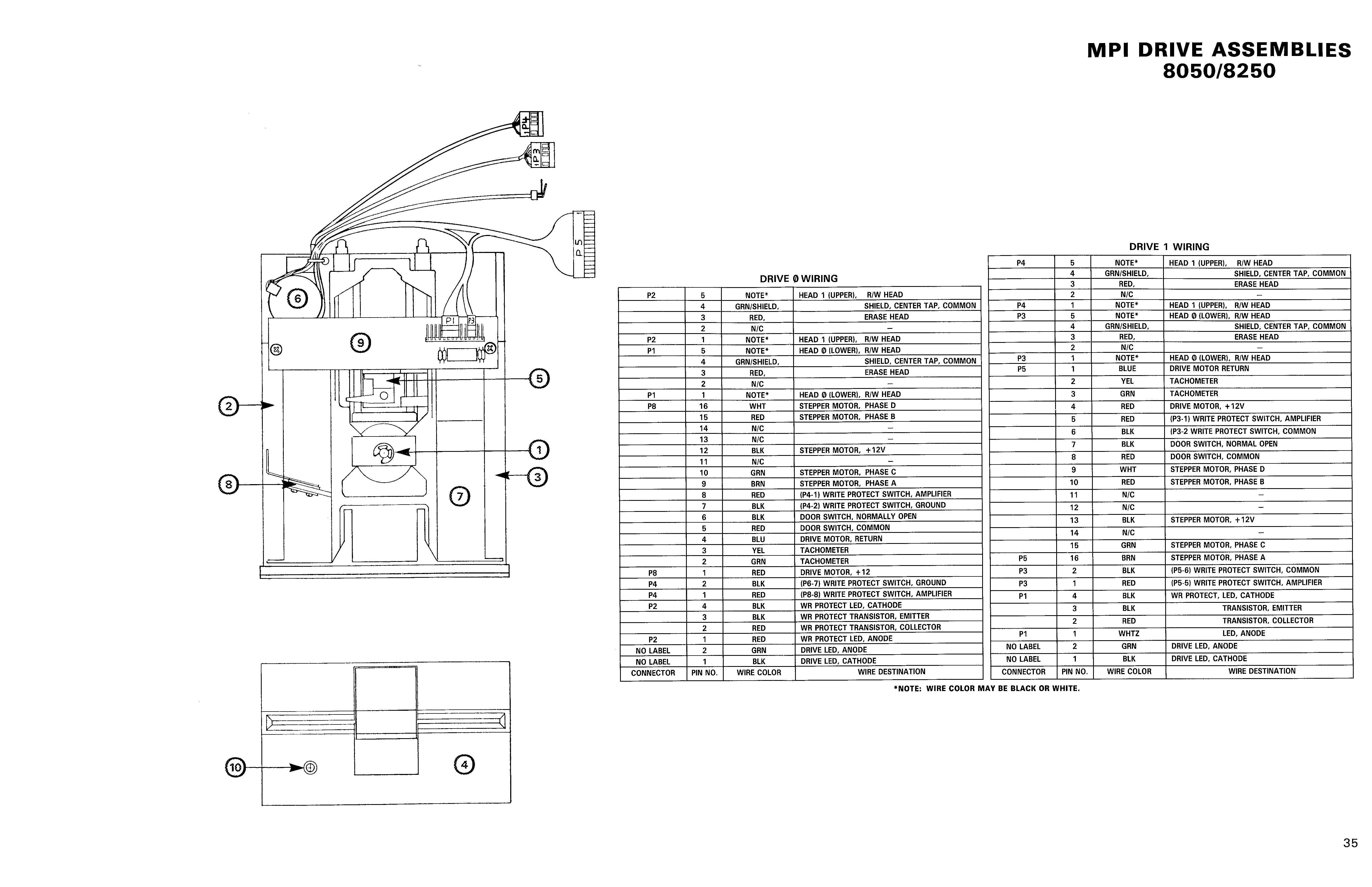
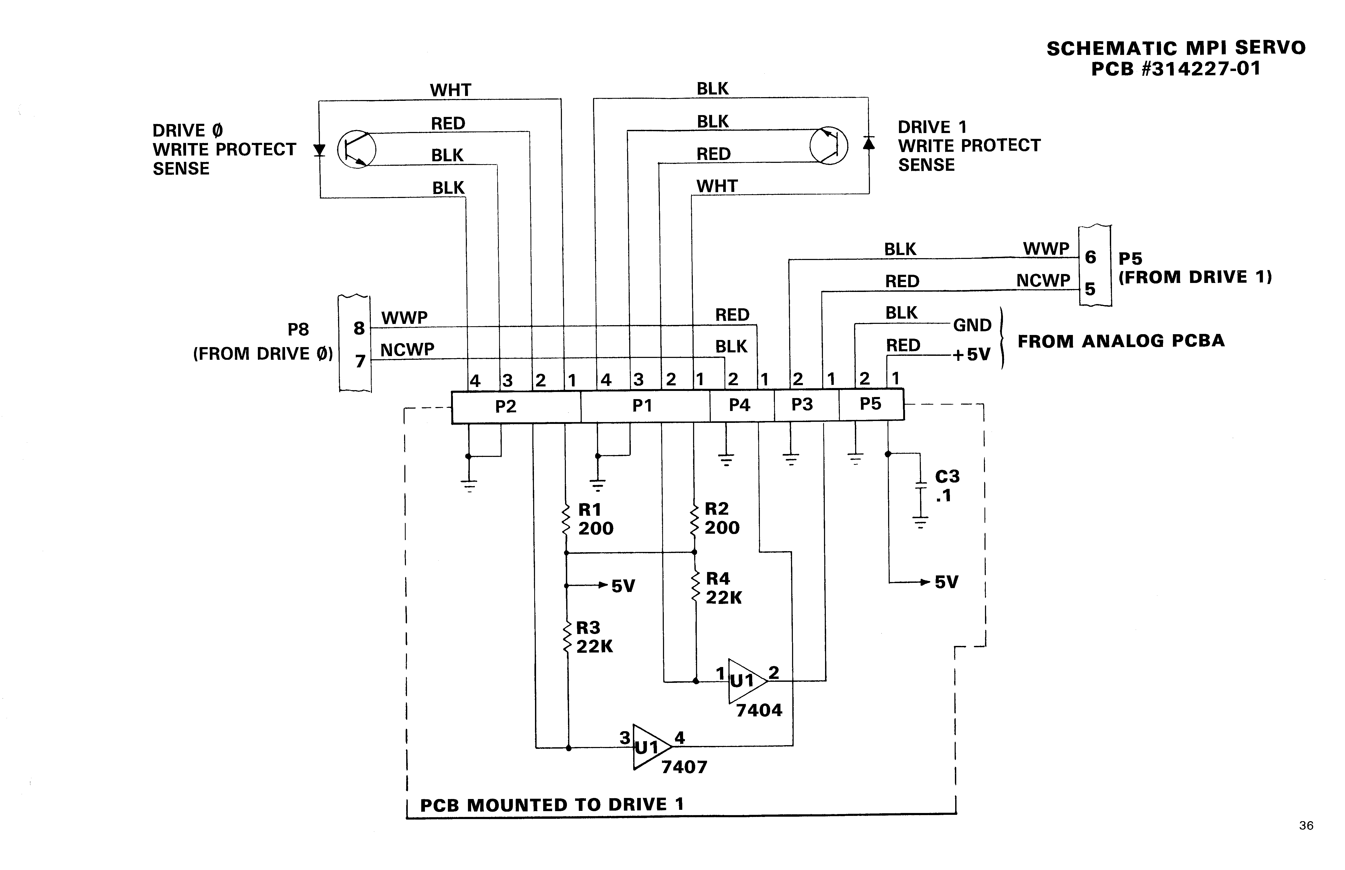
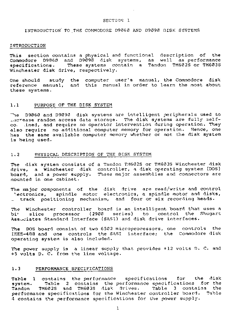
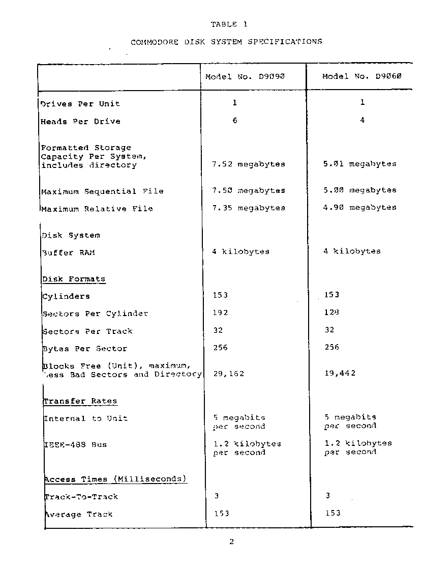
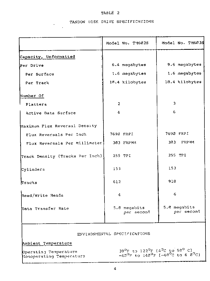
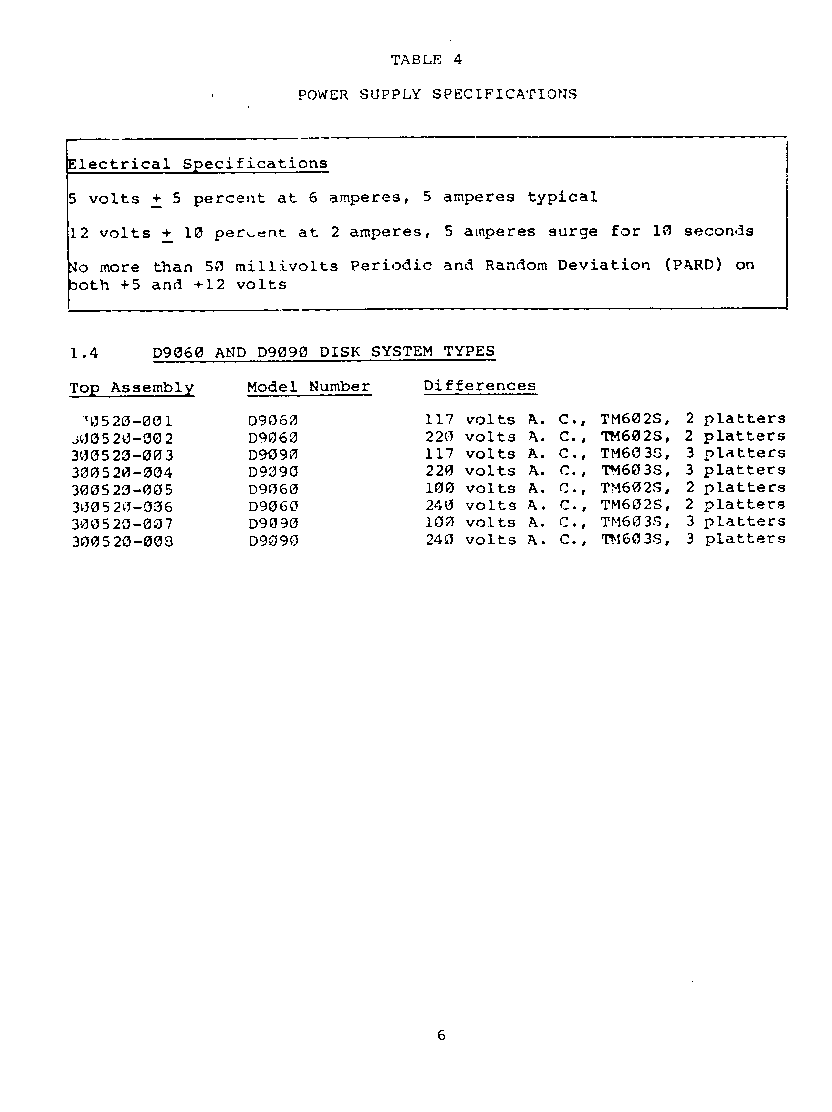
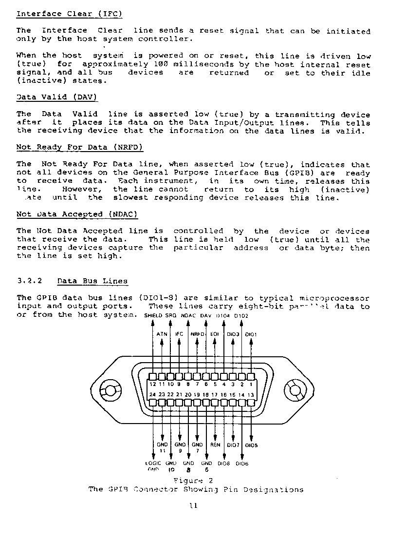
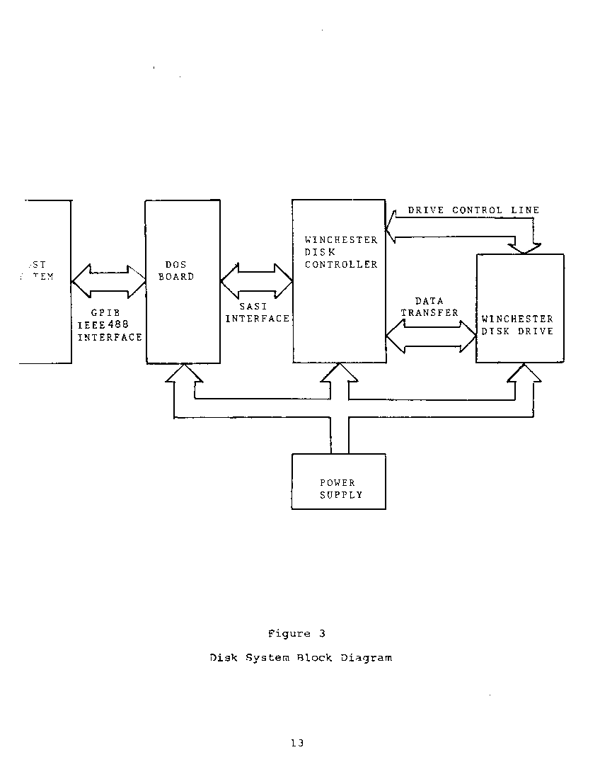
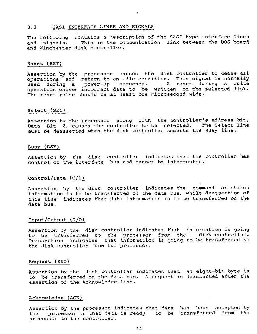
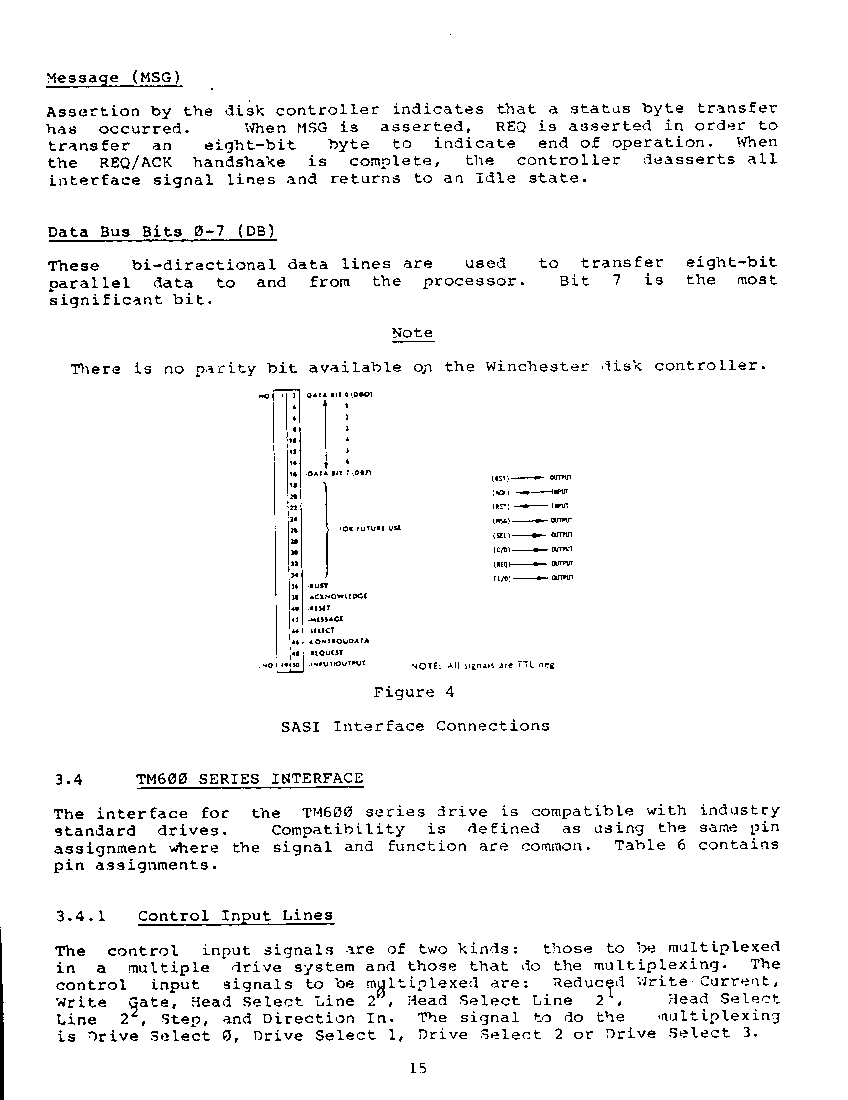
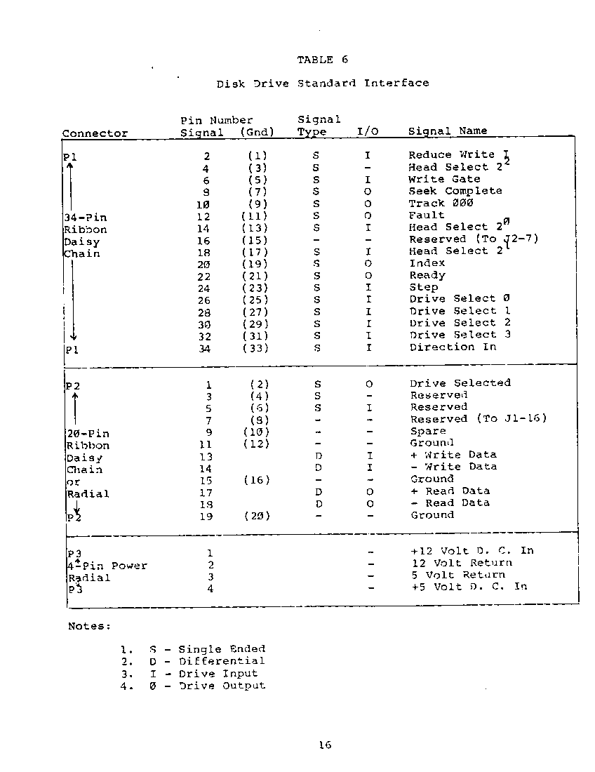
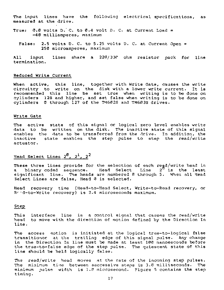
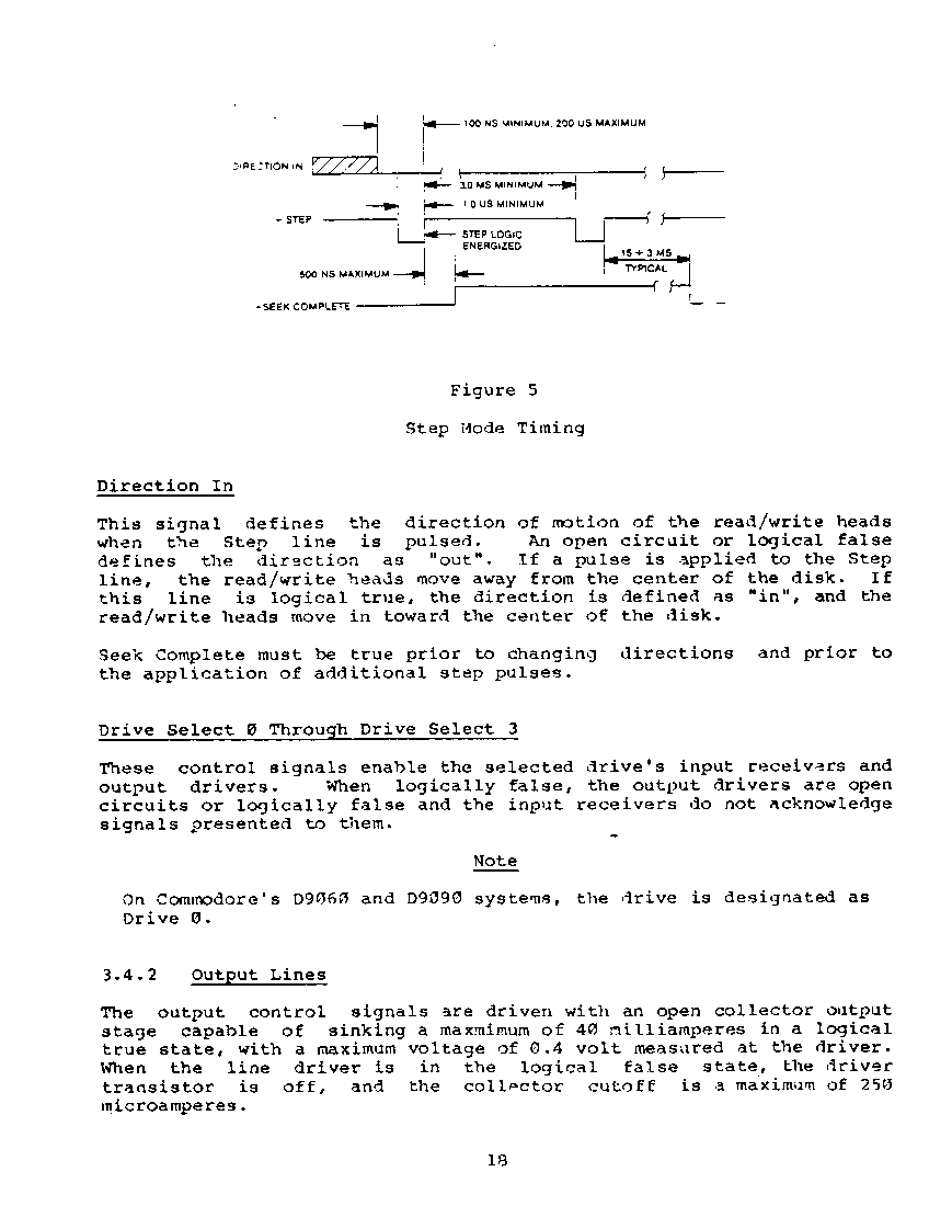
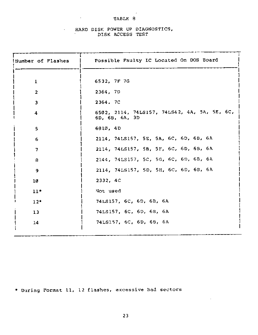
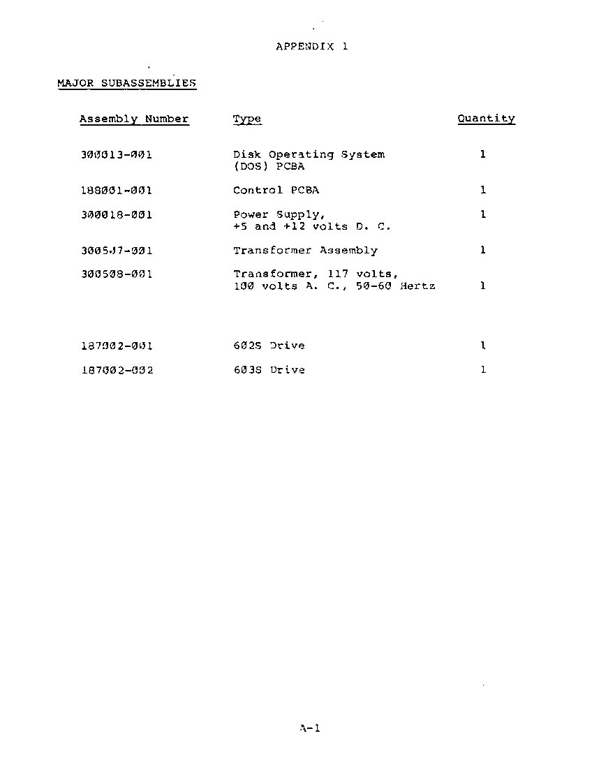
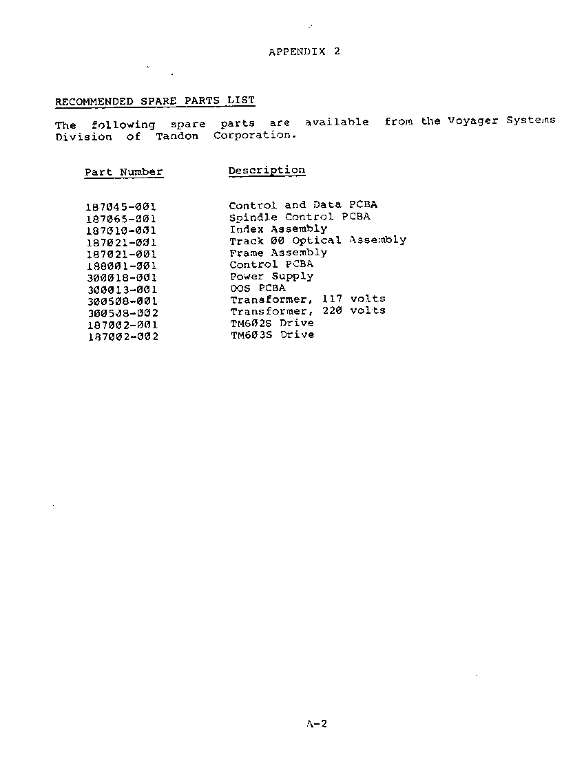
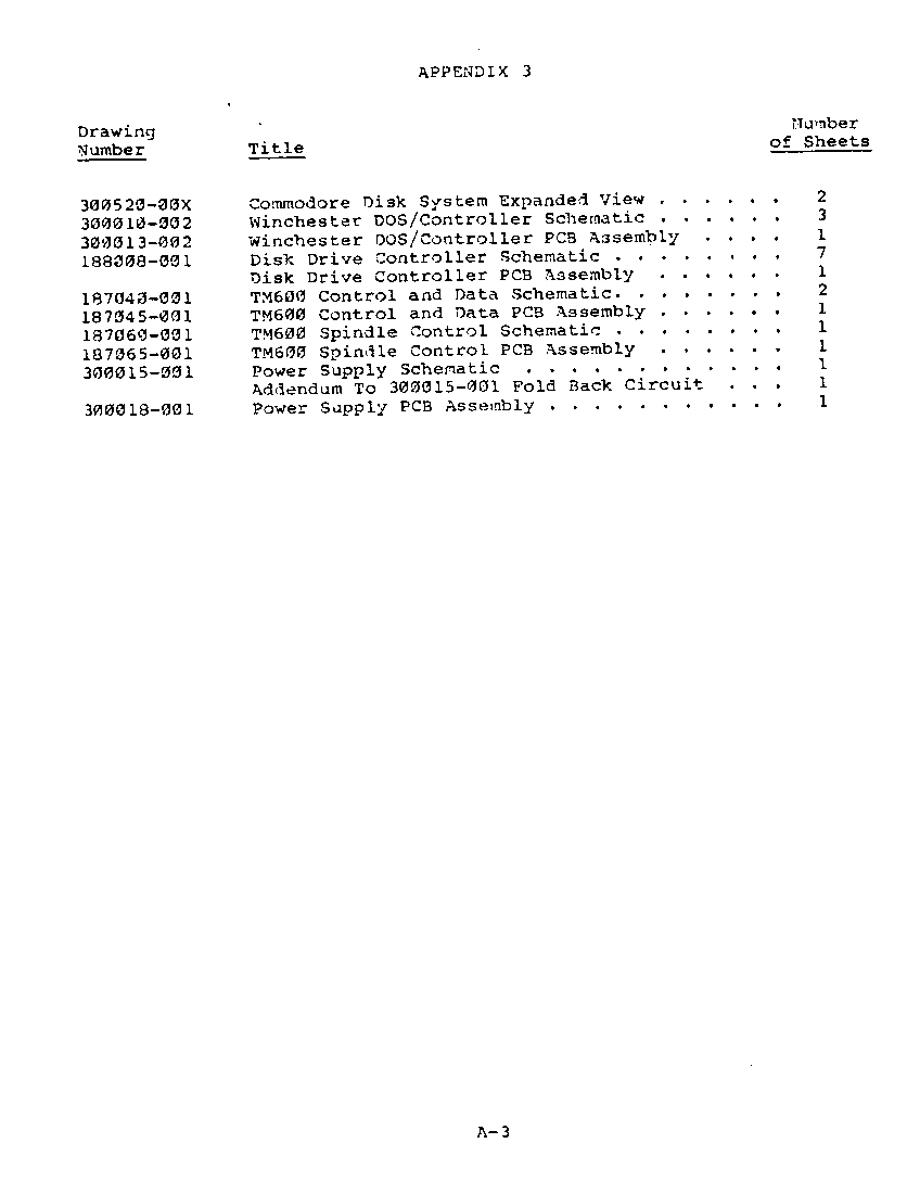
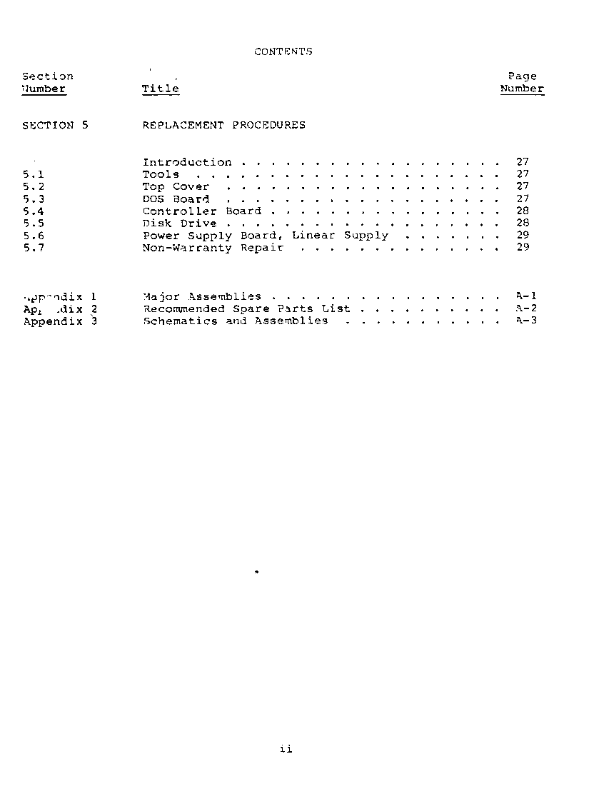
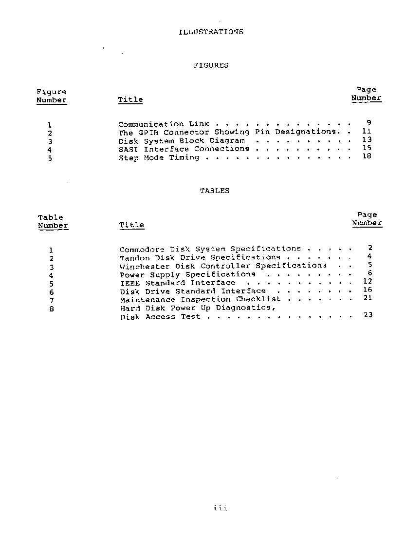
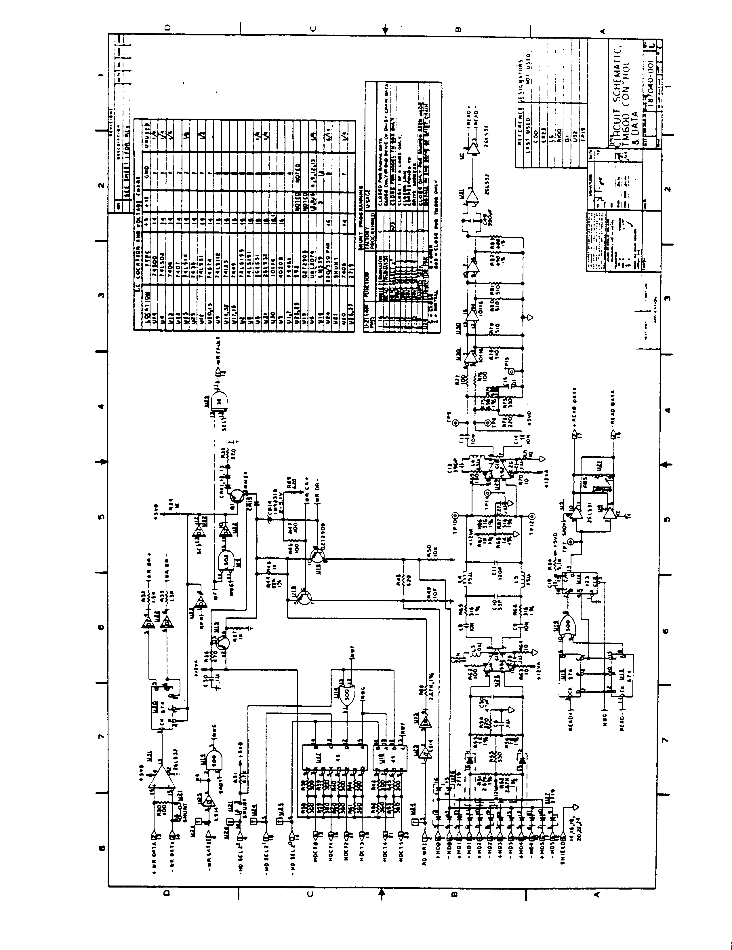
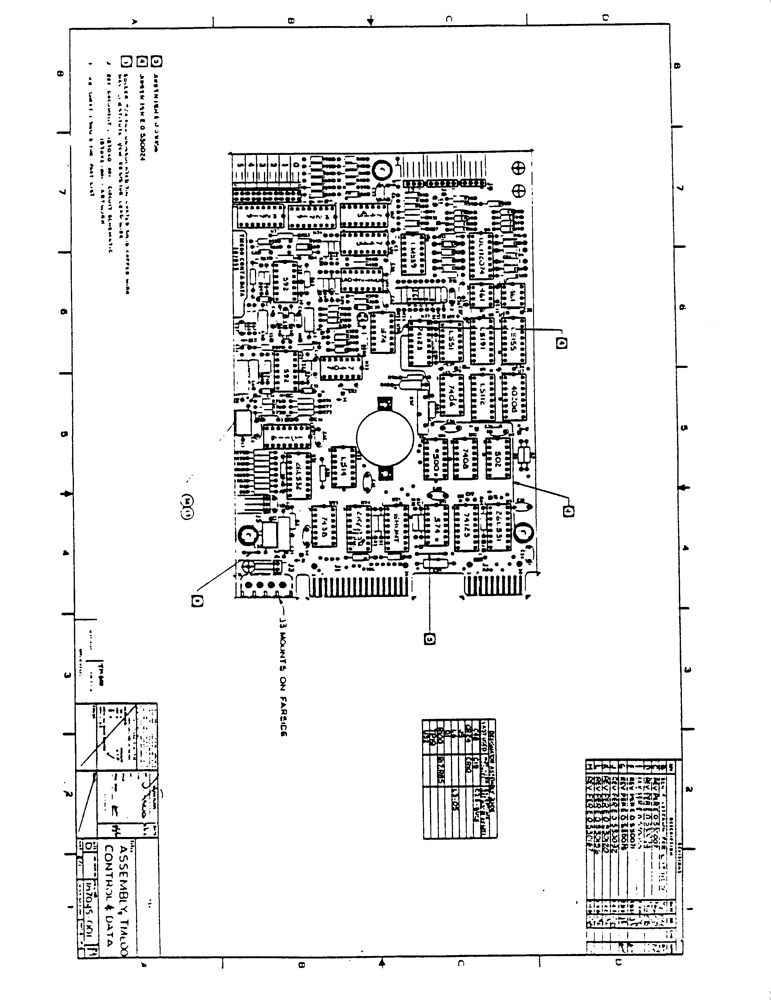
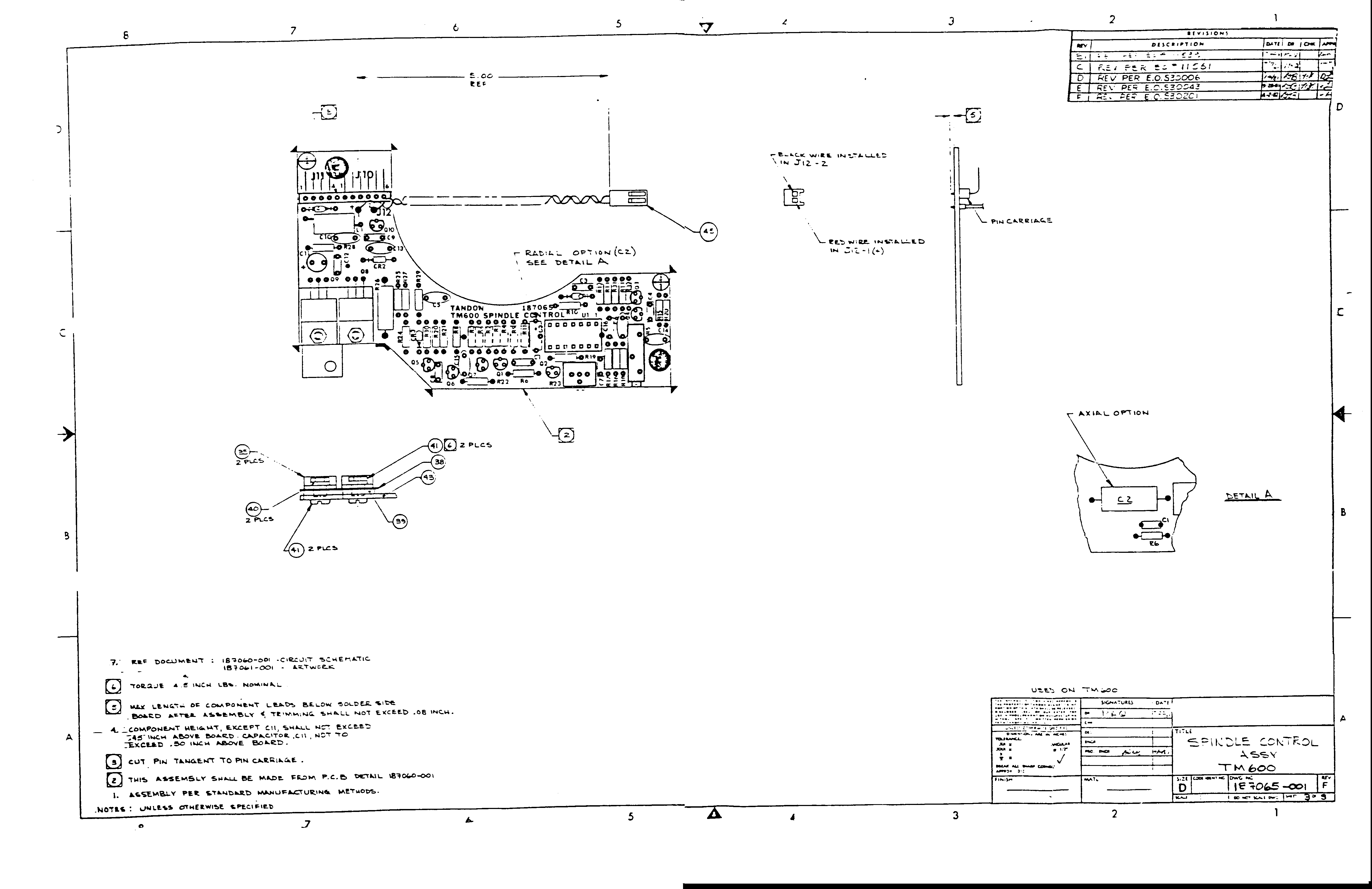
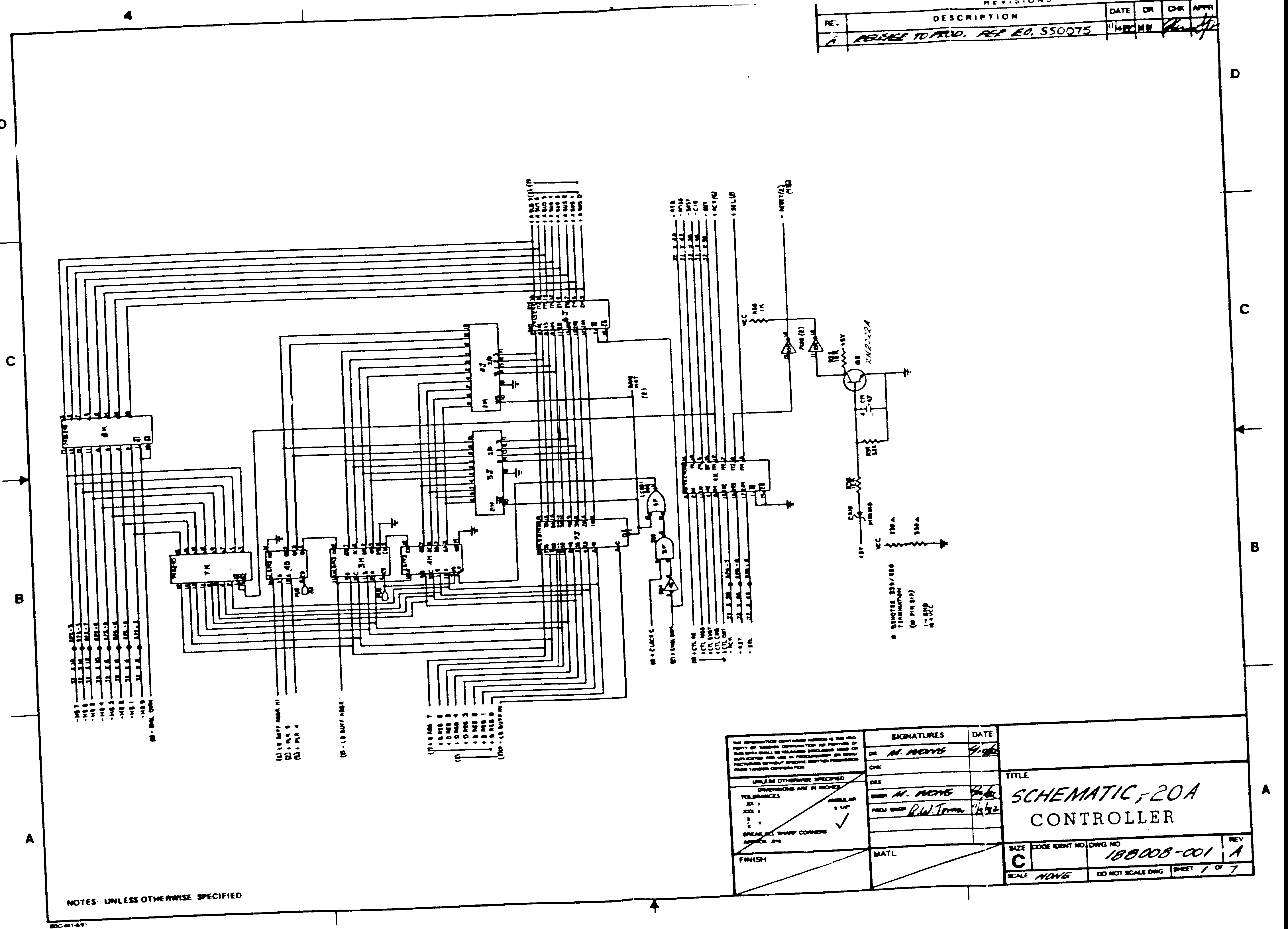
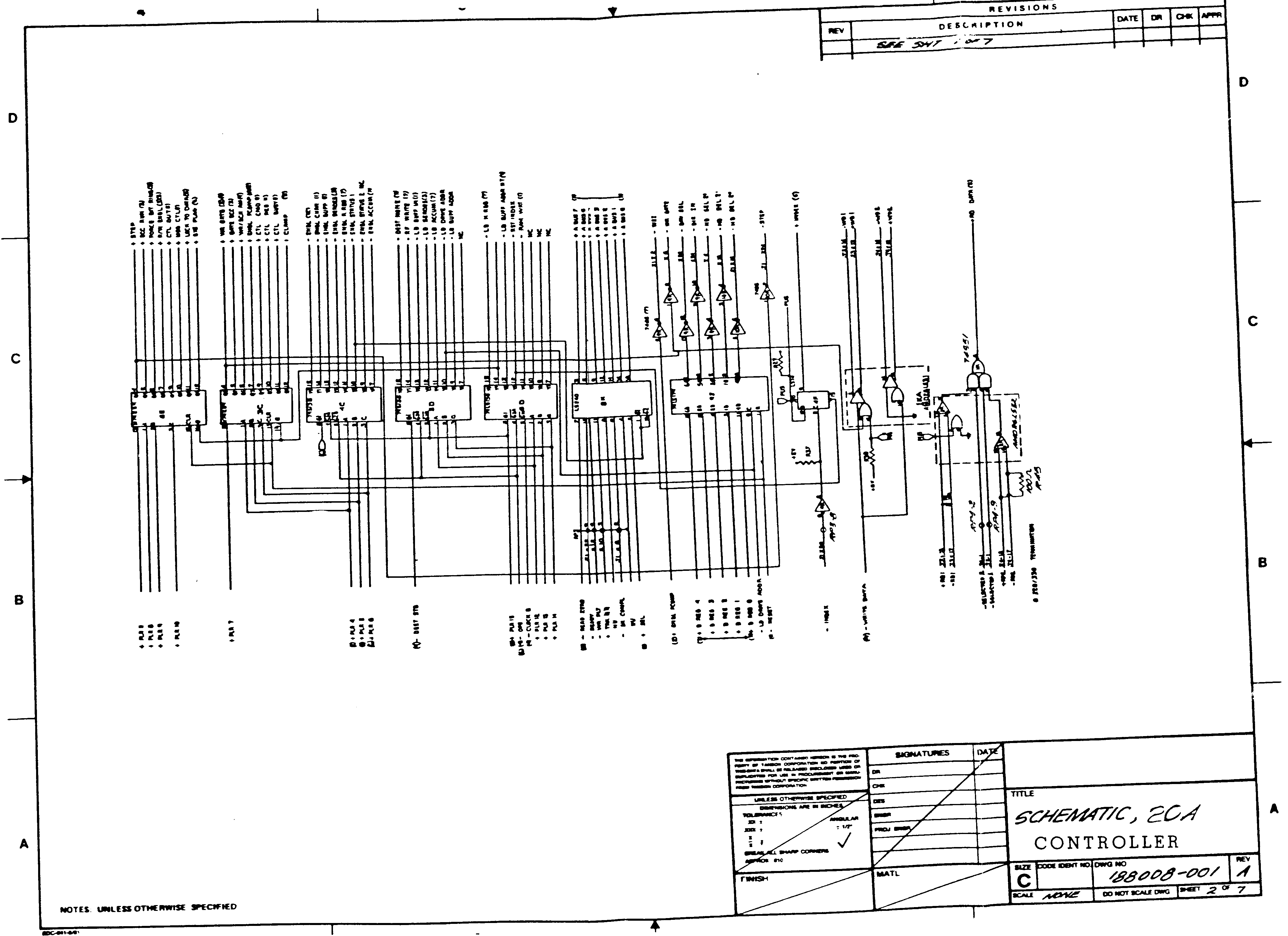
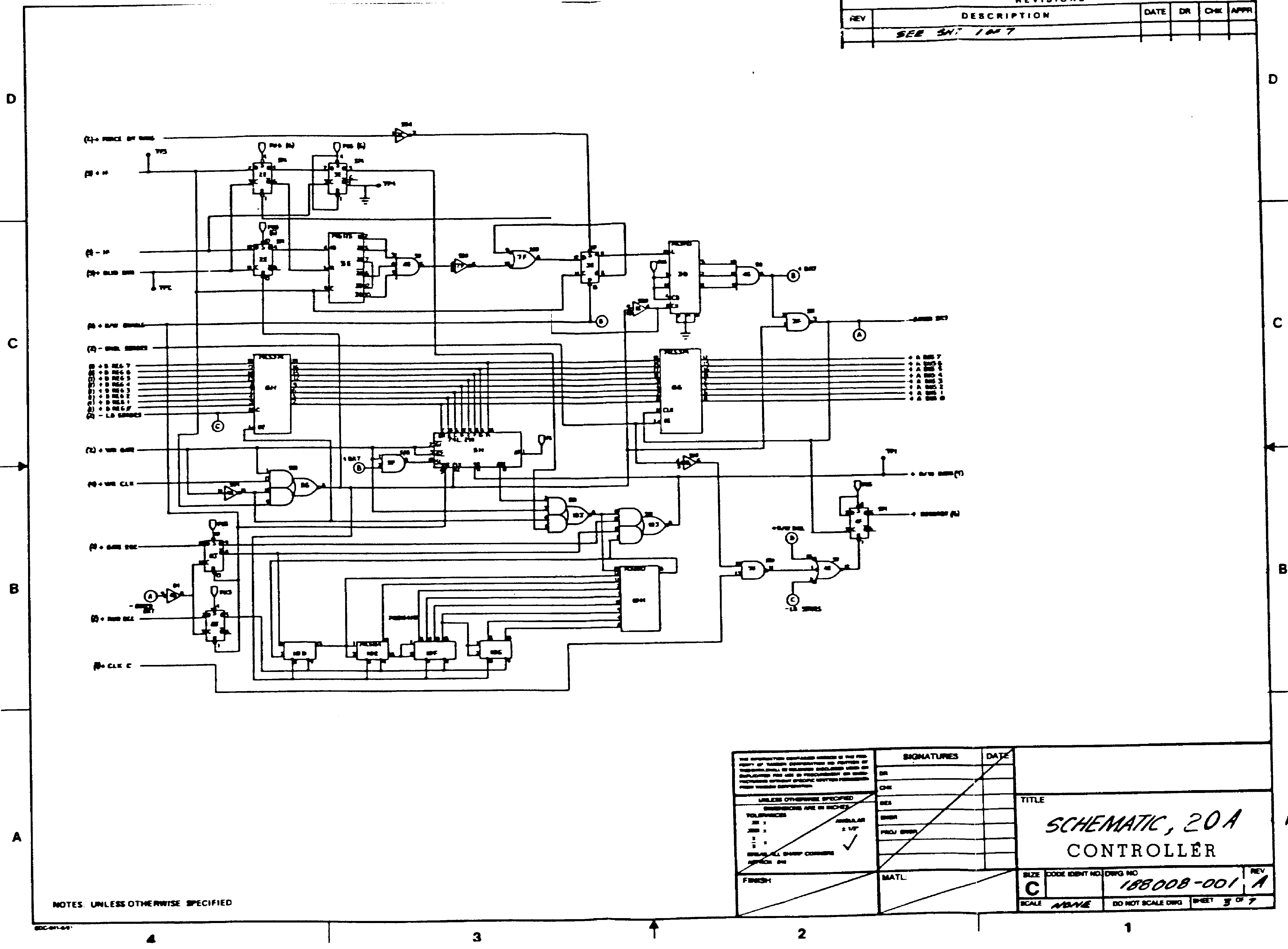
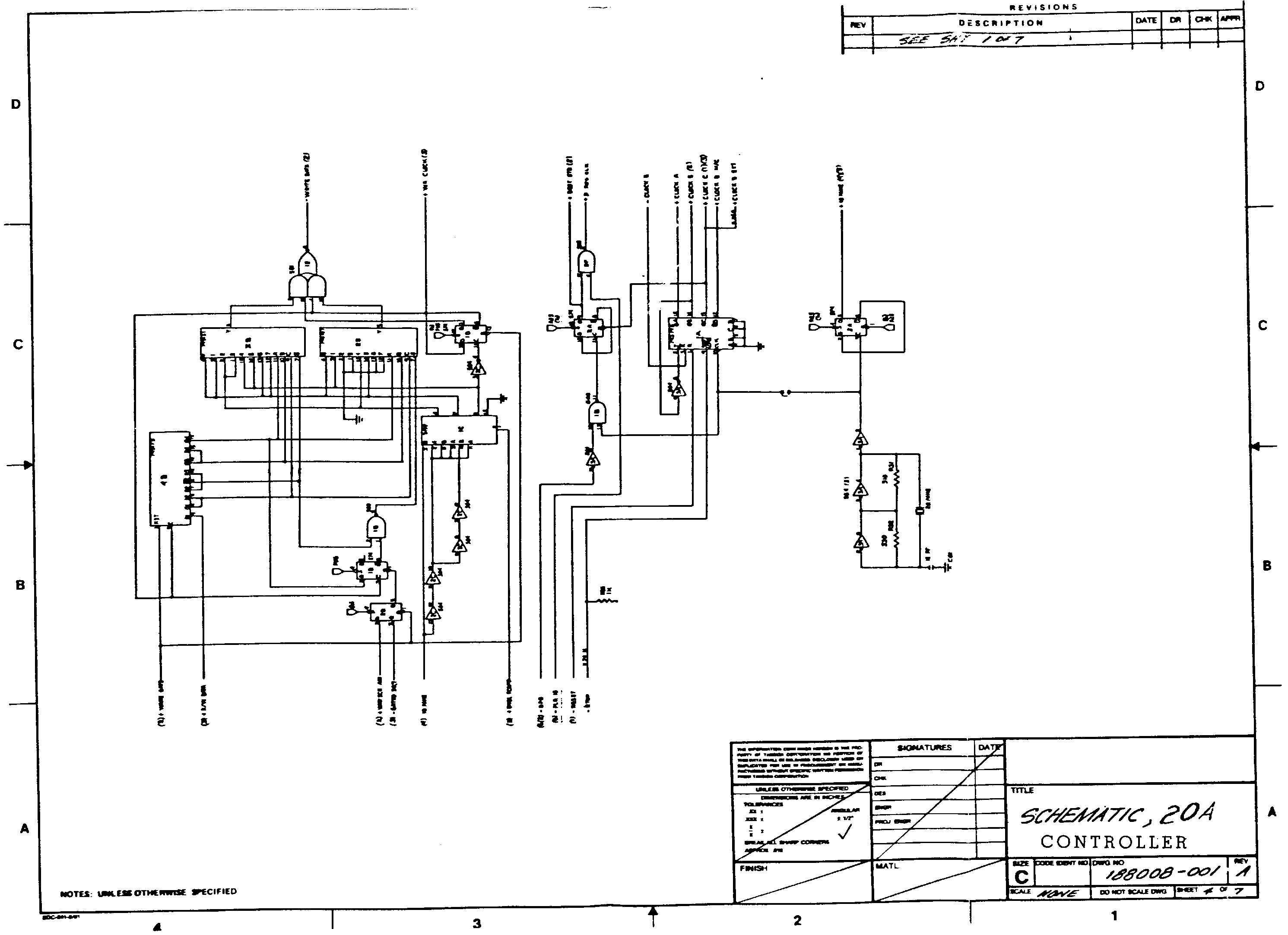
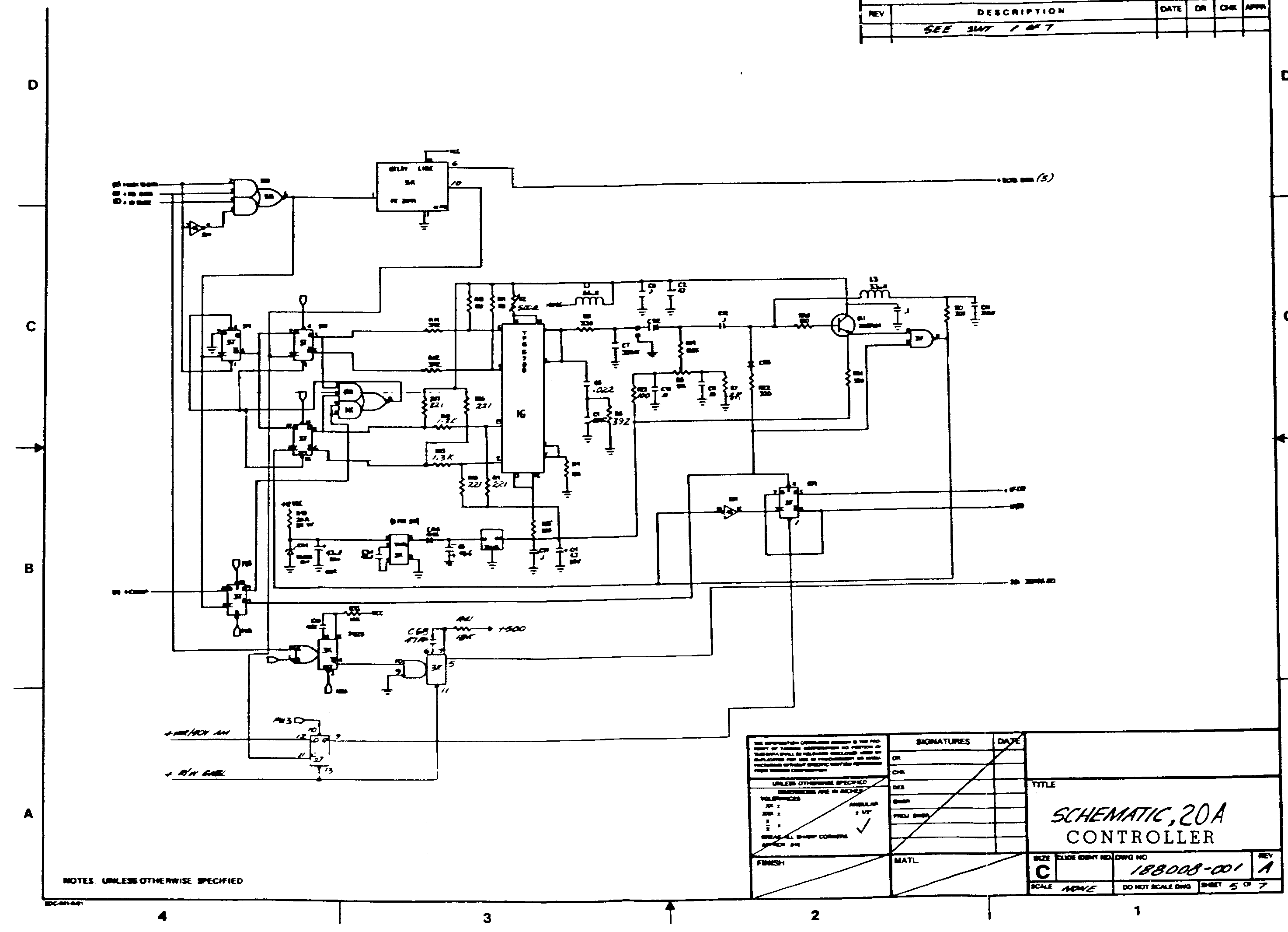
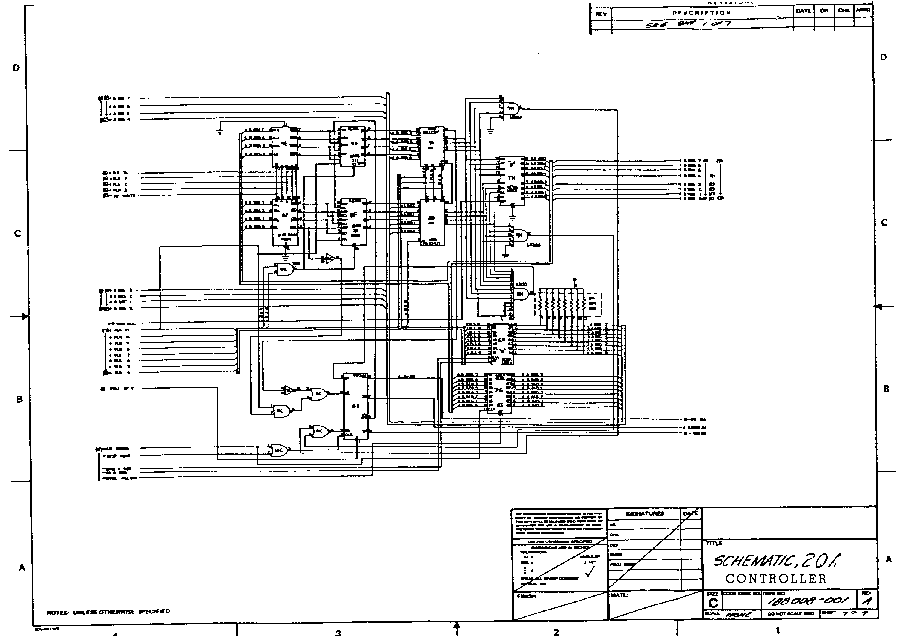
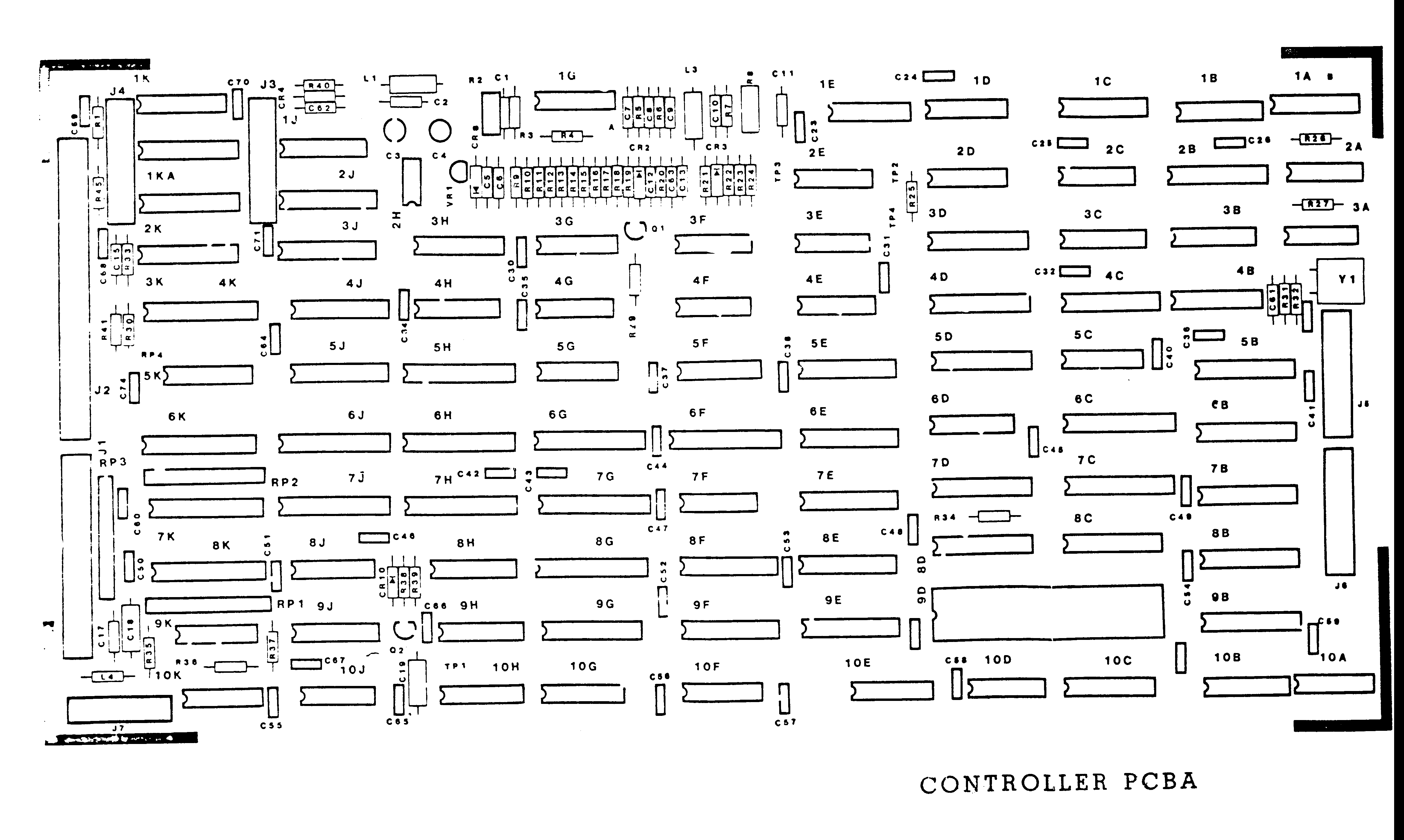
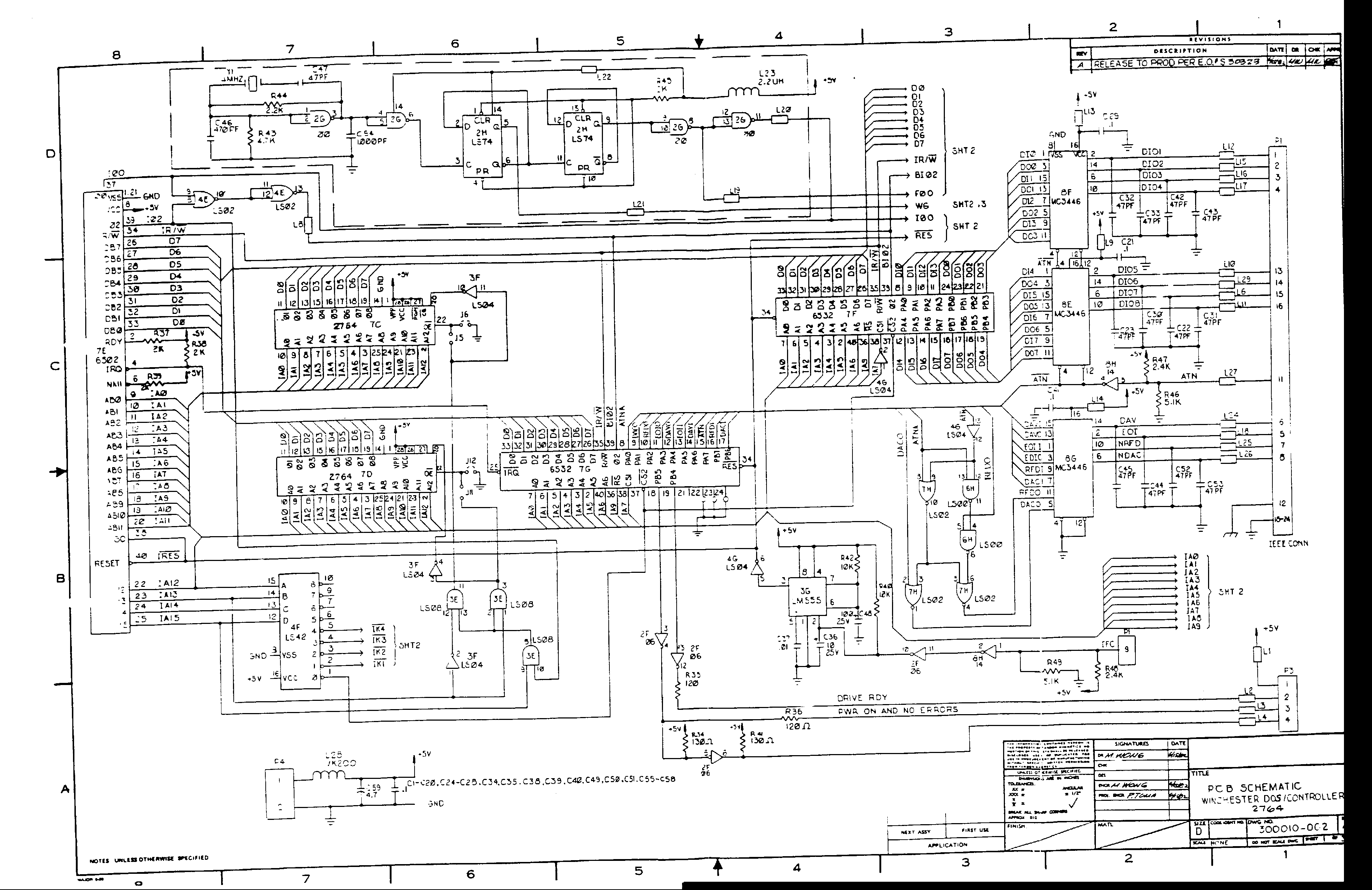
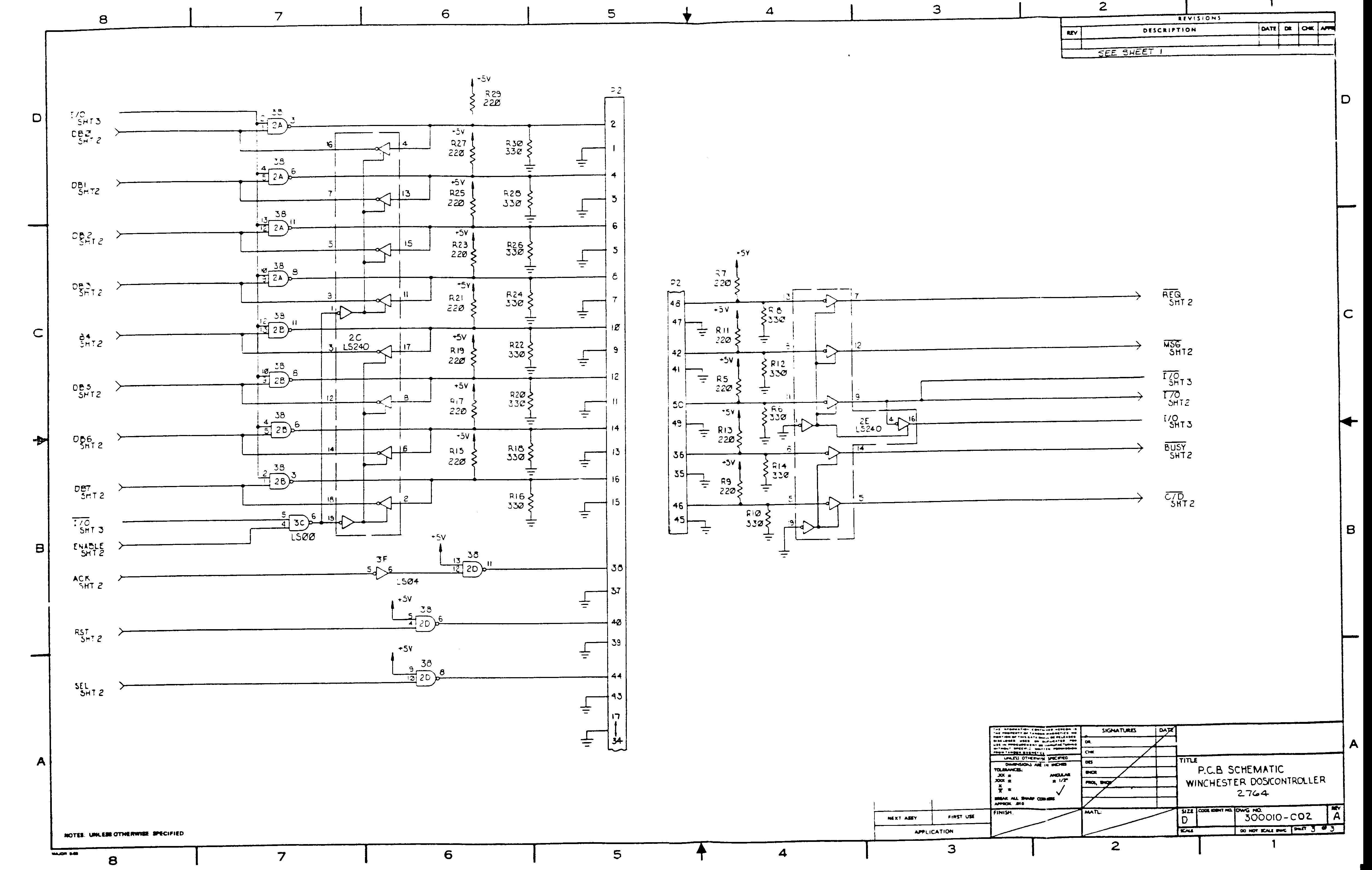
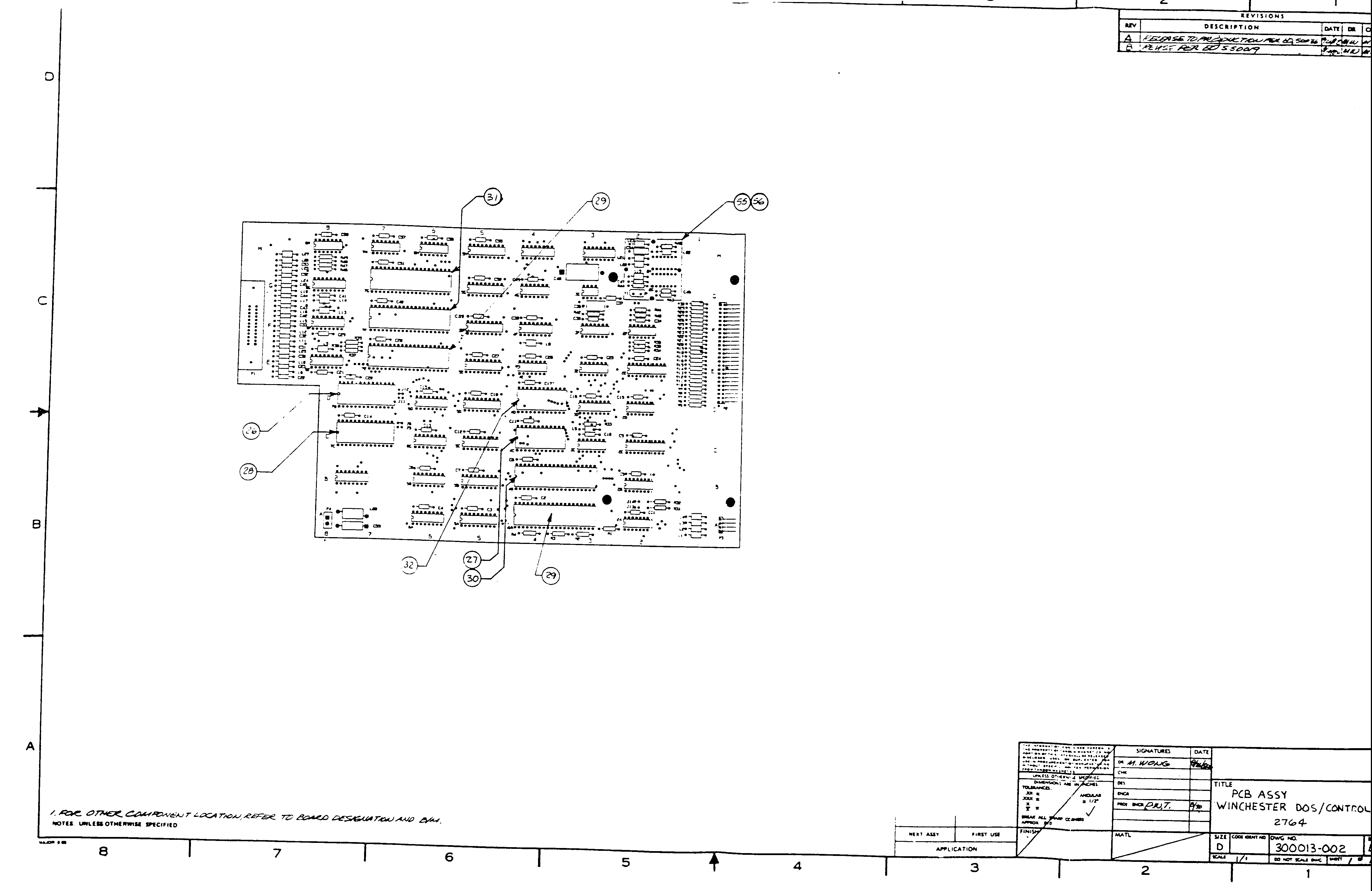
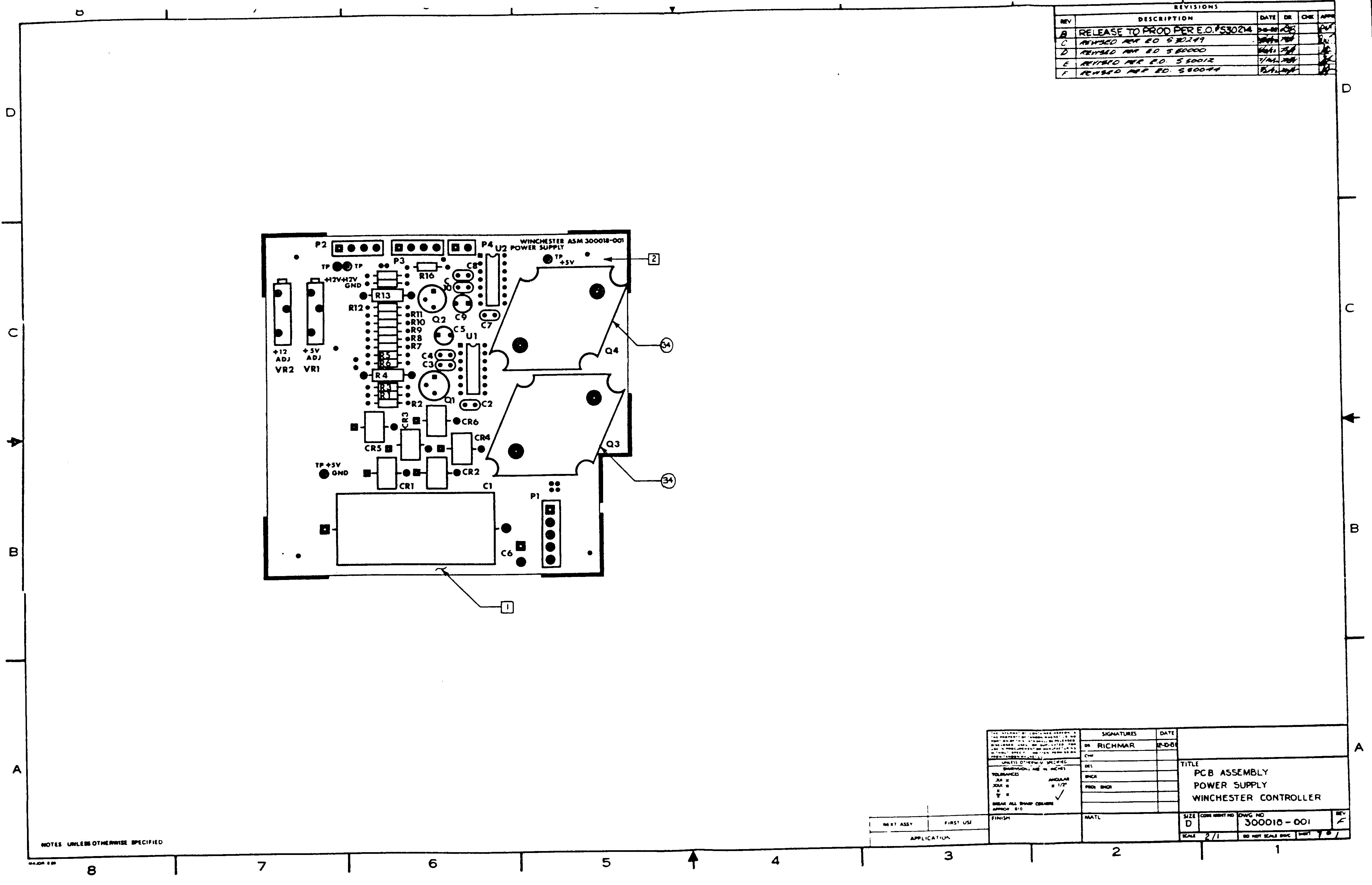
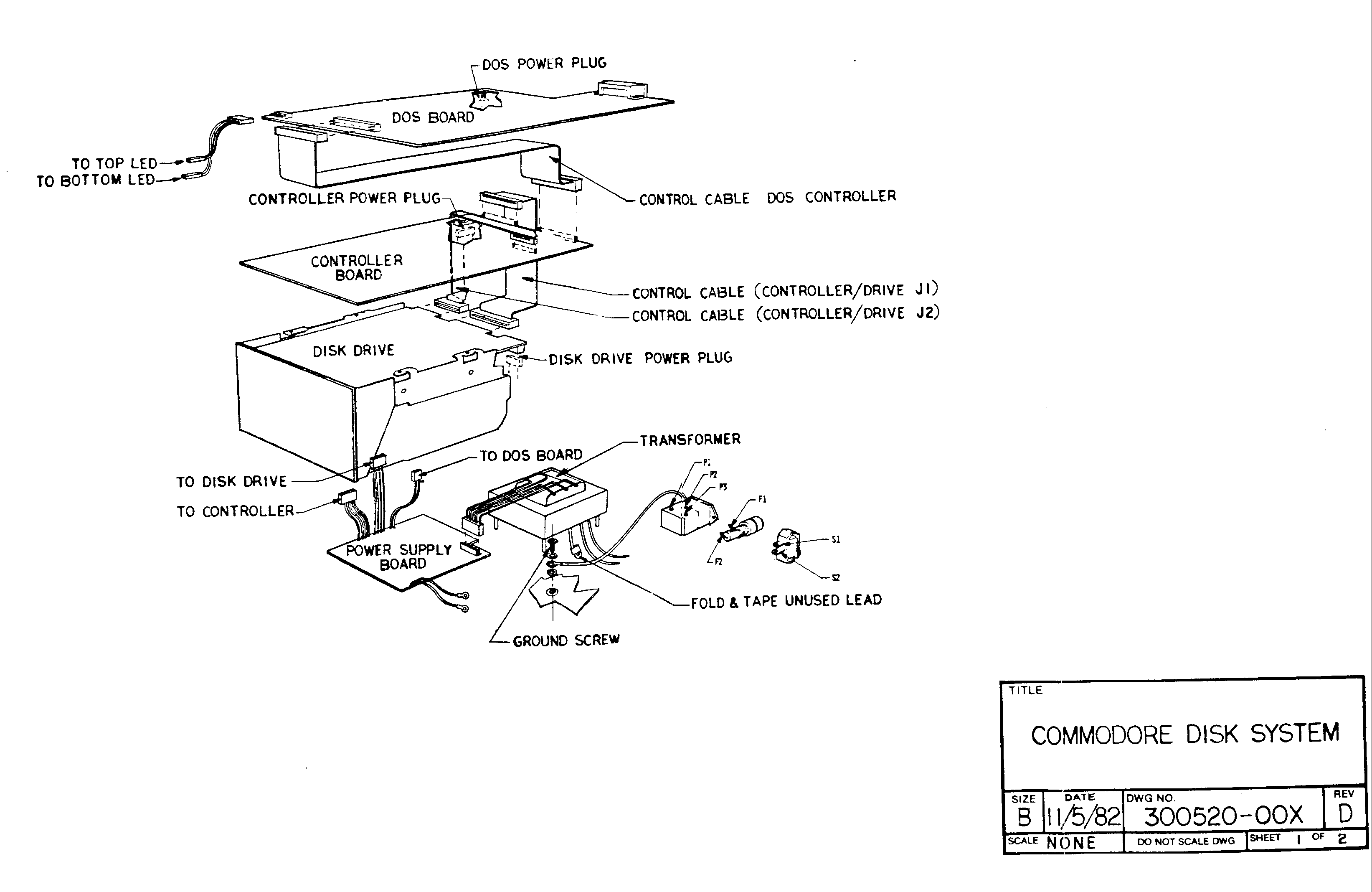
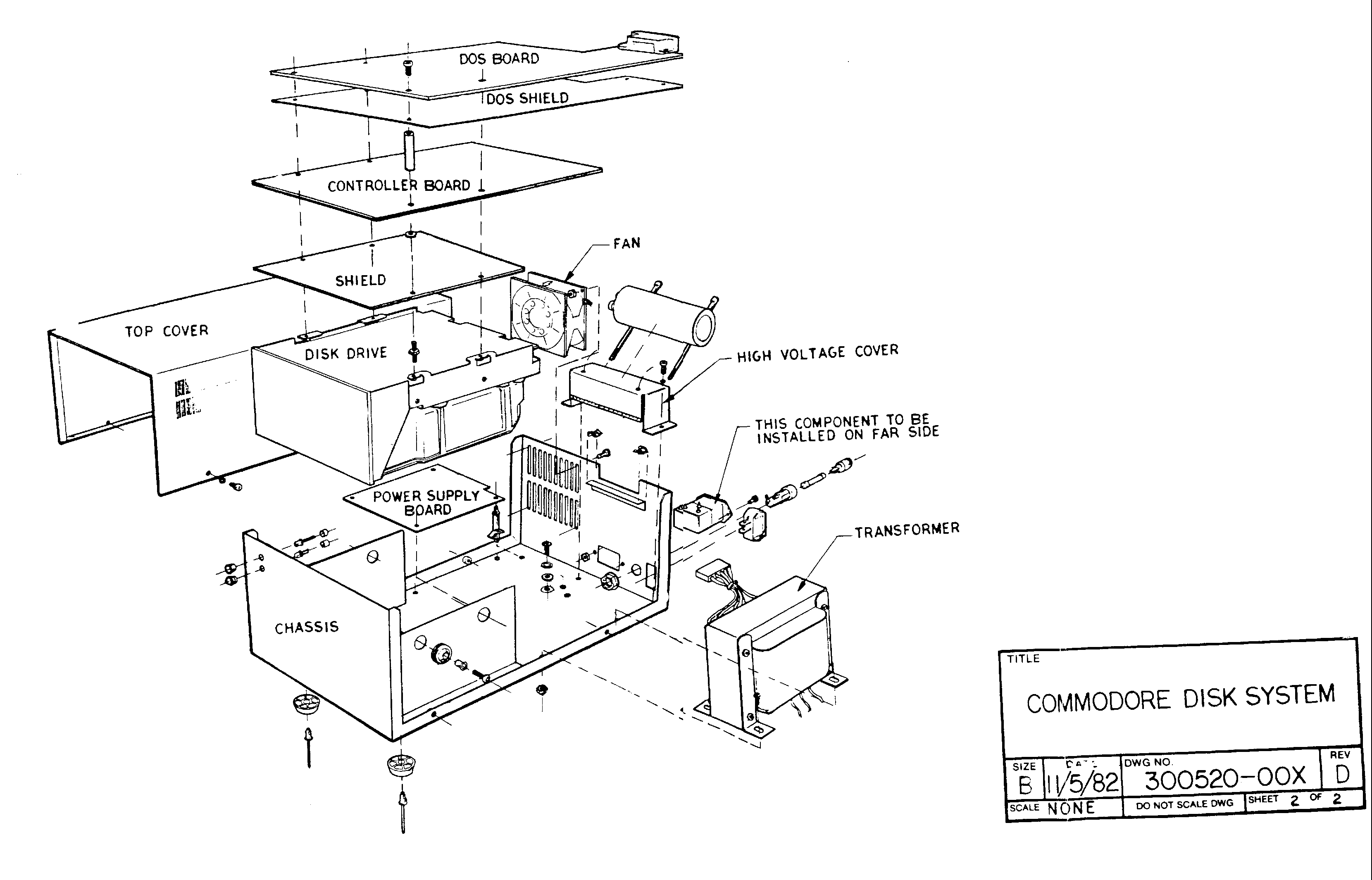
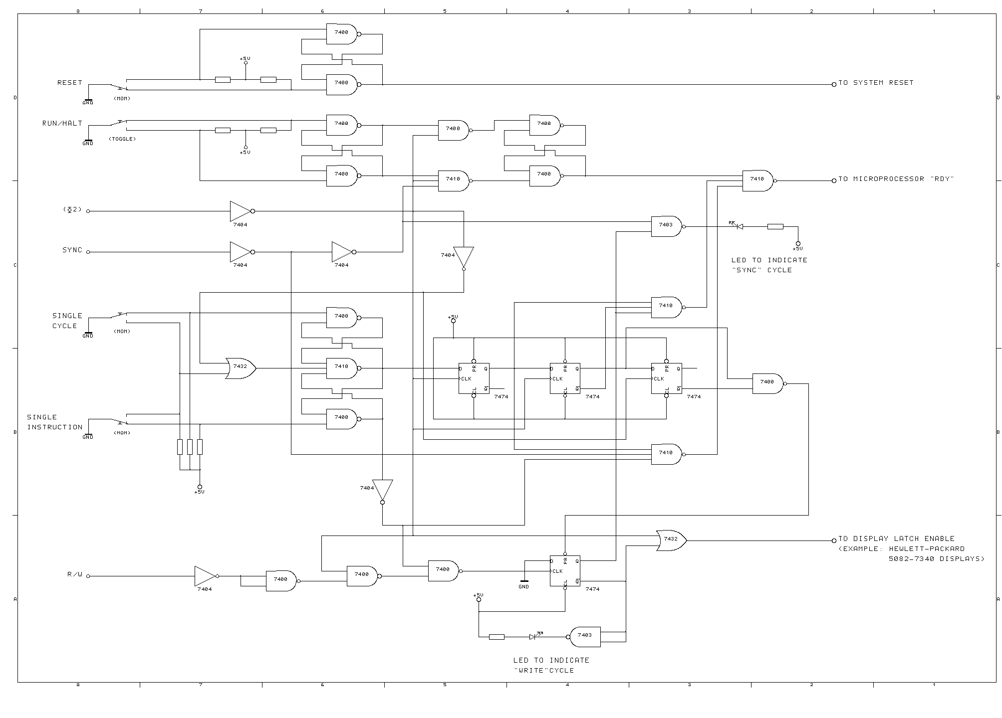
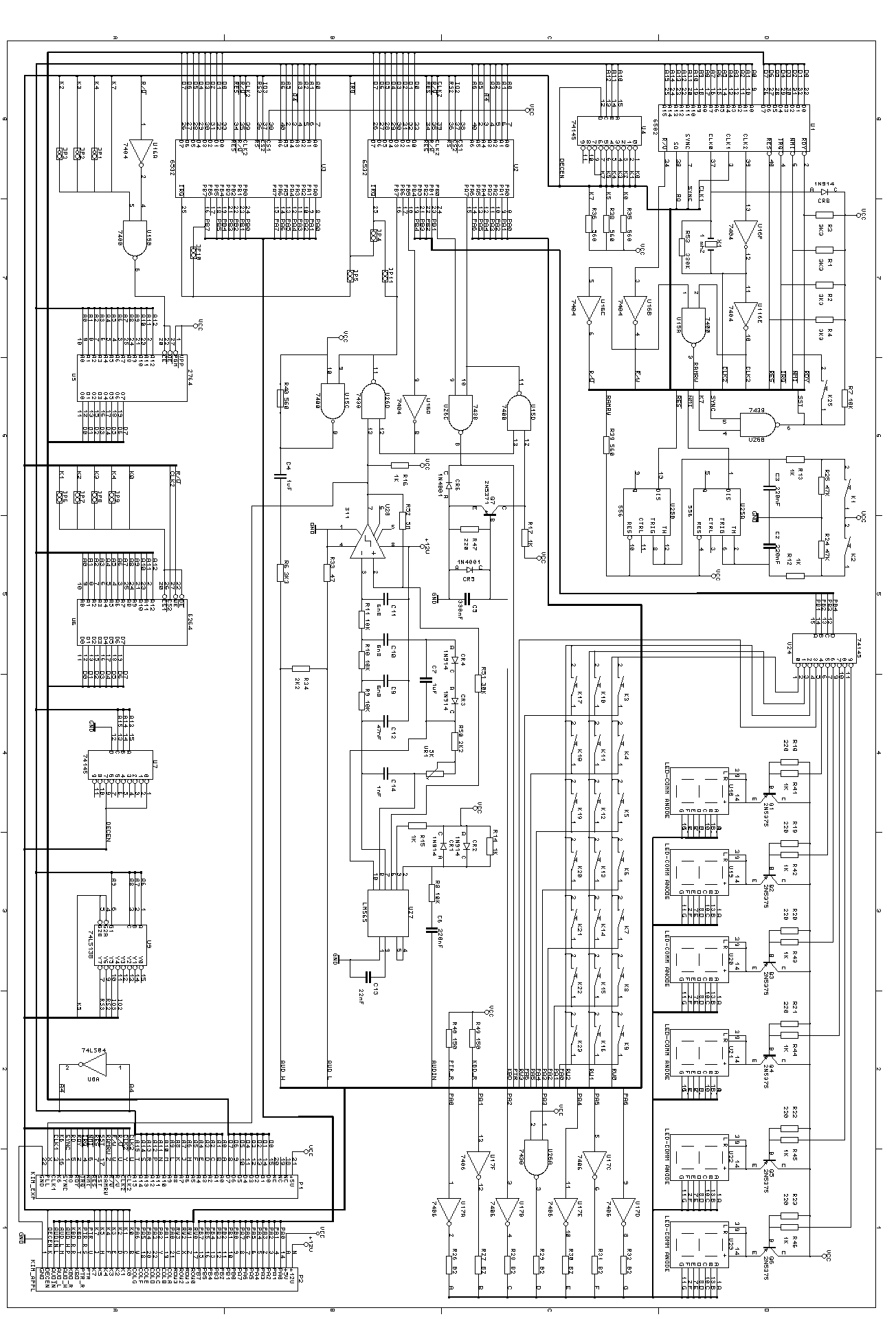
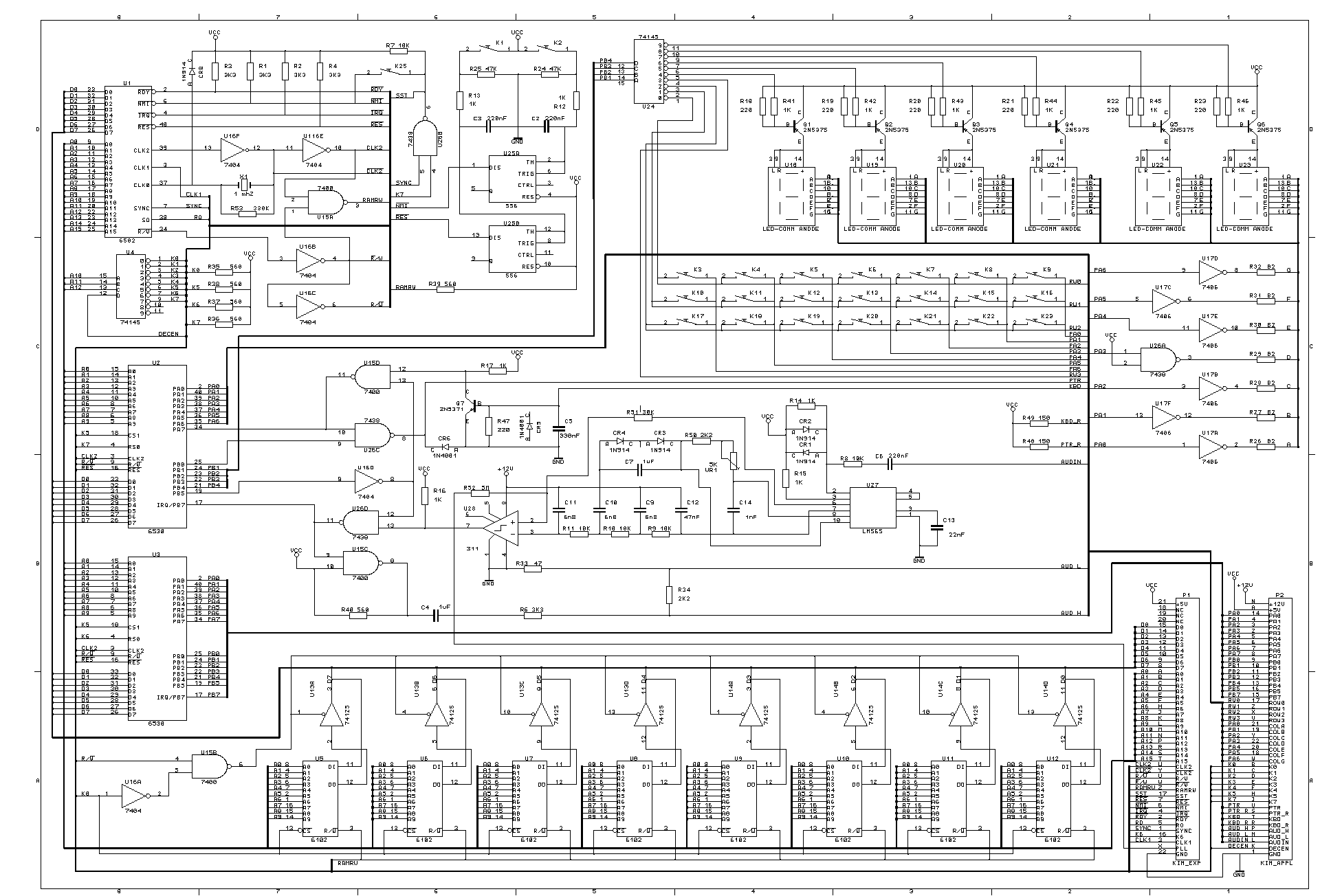
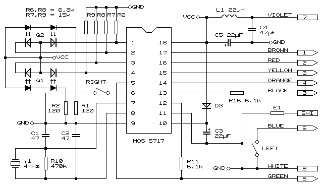
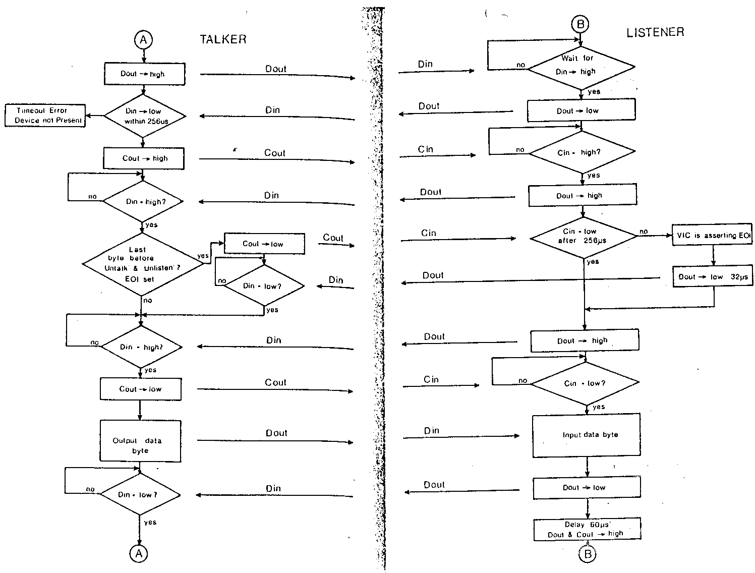
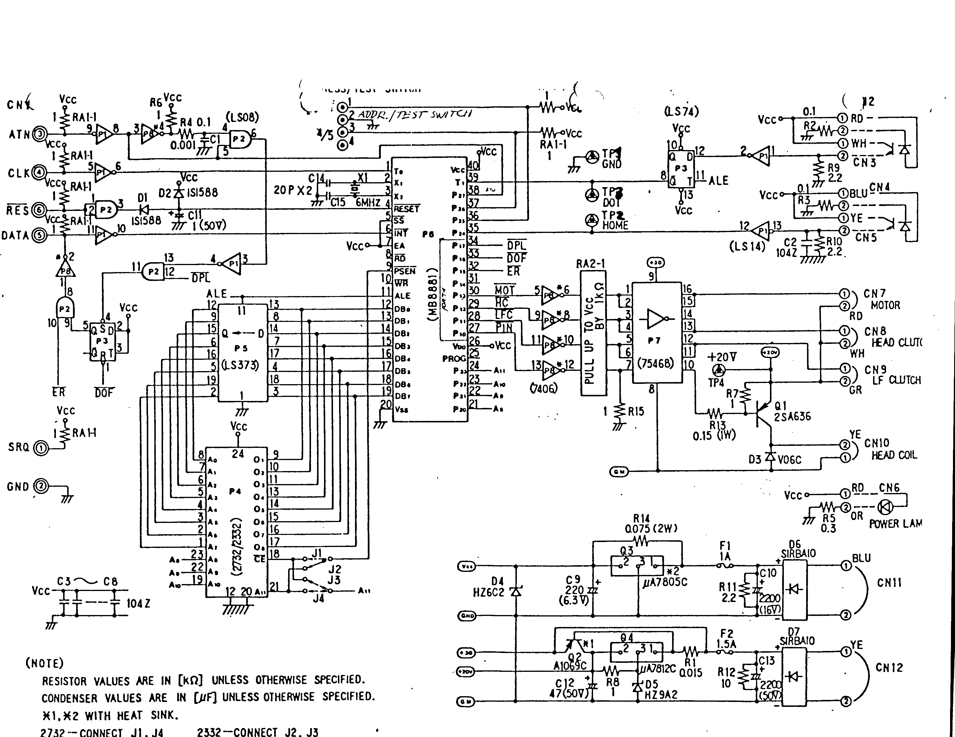
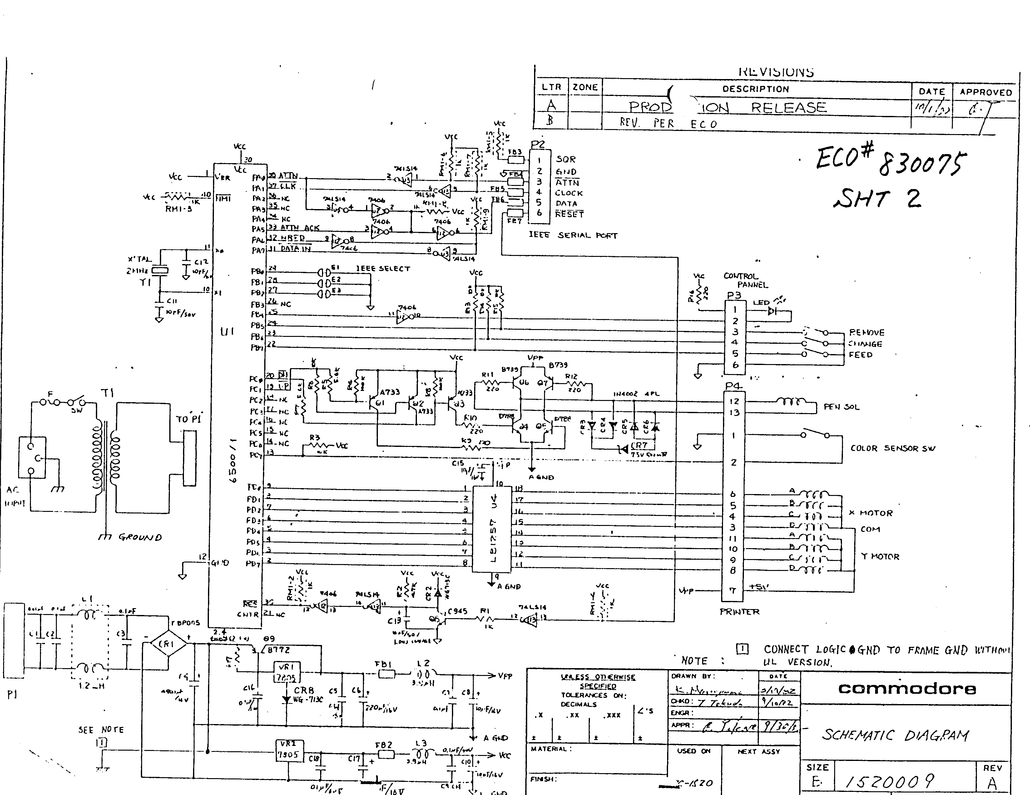
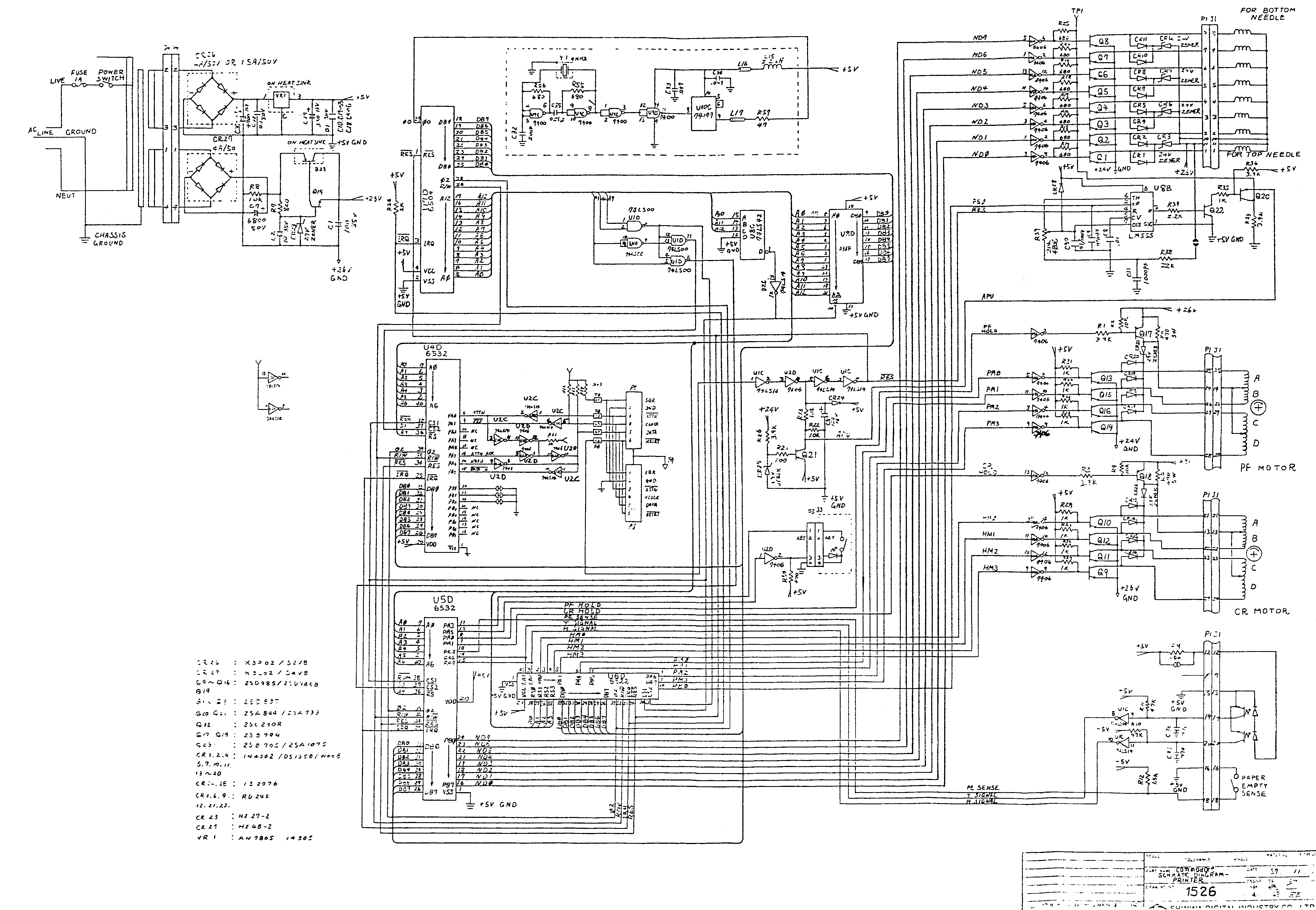
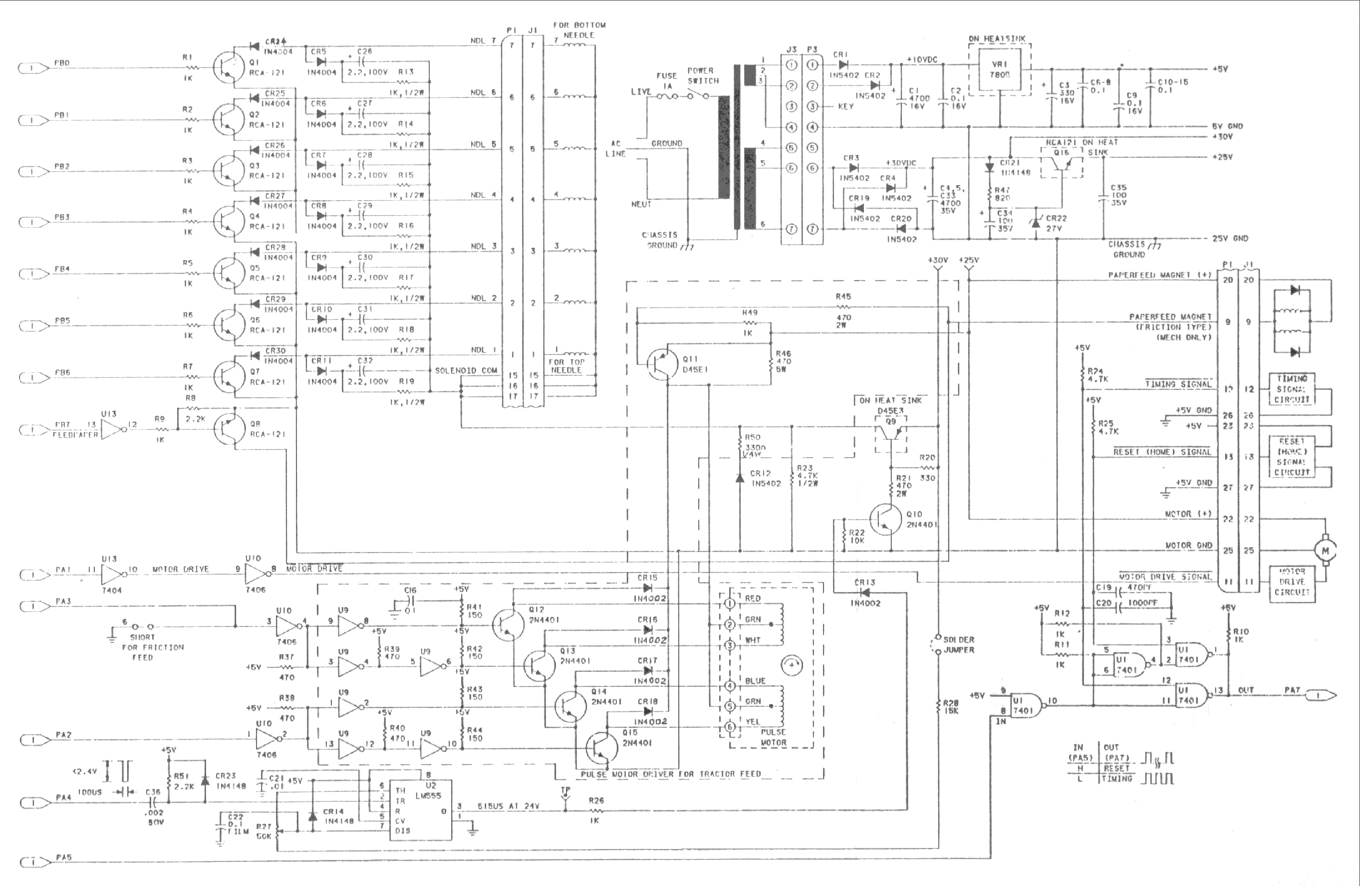